

Datasheet STPS3L60U, STPS3L60RL, STPS3L60QRL, STPS3L60Q Datasheet (SGS Thomson Microelectronics)
Page 1
®
MAIN PRODUCT CHARACTERISTICS
STPS3L60/Q/U
POWER SCHOTTKY RECTIFIER
I
F(AV)
V
RRM
3A
60 V
Tj (max) 150°C
(max) 0.61 V
V
F
FEATURES AND BENEFITS
NEGLIGIBLE SWITCHING LOSSES
■
LOW THERMAL RESISTANCE
■
AVALANCHE CAPABILITY SPECIFIED
■
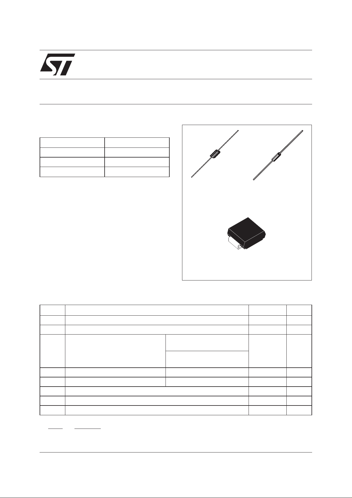
DO-201AD
STPS3L60
DO-15
STPS3L60Q
DESCRIPTION
Axial and Surface Mount Power Schottky rectifier
suited for Switch Mode Power Supplies and high
frequency DC to DC converters. Packaged in
DO-201AD, DO-15 and SMB, this device is
intended for use in low voltage, high frequency
inverters and small battery chargers.
SMB
STPS3L60U
For applications where there are space
constraints, e.g Telecom battery charger.
ABSOLUTE RATINGS (limiting values)
Symbol Parameter Value Unit
V
RRM
I
F(RMS)
I
F(AV)
Repetitive peak reverse voltage
RMS forward current
Average forward current TL= 105°C δ = 0.5
60 V
10 A
3A
(DO-201AD, SMB)
T
= 75°C δ = 0.5
L
(DO-15)
I
FSM
P
ARM
T
stg
T
j
dV/dt
Surge non repetitive forward current tp= 10 ms Sinusoidal
Repetitive peak avalanche power tp = 1µs Tj = 25°C
Storage temperature range
Maximum operating junction temperature *
Critical rate of rise of reverse voltage
100 A
2000 W
- 65 to + 150 °C
150 °C
10000 V/µs
dPtot
*:
<
dTj Rth j a
July 2003 - Ed: 5A
thermal runaway condition for a diode on its ownheatsink
−1()
1/6
Page 2
STPS3L60/Q/U
THERMAL RESISTANCES
Symbol Parameter Value Unit
R
th(j-l)
Junction to leads Lead length = 10 mm DO-201AD
SMB
DO-15
STATIC ELECTRICAL CHARACTERISTICS
Symbol Parameter Tests conditions Min. Typ. Max. Unit
I
*
R
V
F
Pulse test : * tp = 380 µs, δ <2%
Reverse leakage current Tj= 25°C VR=V
= 100°C
T
j
= 125°C
T
j
*
Forward voltage drop Tj= 25°C IF=3A
= 100°C
T
j
= 125°C
T
j
= 25°C IF=6A
T
j
= 100°C
T
j
= 125°C
T
j
RRM
20 °C/W
20
35
150 µA
415mA
14 30
0.62 V
0.53 0.61
0.51 0.59
0.79
0.62 0.71
0.6 0.69
To evaluate the maximum conduction losses use the following equation:
P=0.44xI
Fig. 1: Average forward power dissipation versus
average forward current.
P (W)
F(AV)
2.5
2.0
1.5
1.0
0.5
0.0
0.0 0.5 1.0 1.5 2.0 2.5 3.0 3.5 4.0
F(AV)
δ = 0.05
+0.05xI
δ = 0.1
δ = 0.2
I (A)
F(AV)
F2(RMS)
δ = 0.5
δ
=tp/T
δ = 1
T
Fig. 2-1: Average forward current versus ambient
temperature (δ = 0.5) (DO-201AD, SMB).
I (A)
F(AV)
3.5
3.0
2.5
2.0
1.5
1.0
tp
0.5
0.0
T
=tp/T
δ
0 25 50 75 100 125 150
tp
R=R
th(j-a) th(j-I)
R =80°C/W
th(j-a)
T (°C)
amb
2/6
Page 3

STPS3L60/Q/U
Fig. 2-2: Average forward current versus ambient
temperature (δ = 0.5) (DO-15).
I (A)
F(AV)
3.5
3.0
2.5
2.0
1.5
1.0
0.5
0.0
R=R
th(j-a) th(j-I)
R =100°C/W
th(j-a)
T
T (°C)
=tp/T
δ
0 25 50 75 100 125 150
tp
amb
Fig. 4: Normalized avalanche power derating
versus junction temperature.
P(t)
ARM p
P (25°C)
ARM
1.2
1
0.8
0.6
0.4
0.2
0
0 25 50 75 100 125 150
T (°C)
j
Fig. 3: Normalized avalanche power derating
versus pulse duration.
P(t)
ARM p
P (1µs)
ARM
1
0.1
0.01
t (µs)
0.001
0.10.01 1
p
10 100 1000
Fig. 5-1: Non repetitive surge peak forward
current versus overload duration (maximum
values) (DO-201AD, SMB).
I (A)
M
12
10
T =25°C
8
6
4
IM
2
0
1E-3 1E-2 1E-1 1E+0
δ=0.5
t
t(s)
a
T =50°C
a
T =100°C
a
Fig. 5-2: Non repetitive surge peak forward
current versus overload duration (maximum
values) (DO-15).
I (A)
M
11
10
9
8
7
6
5
4
3
IM
2
1
0
1.E-03 1.E-02 1.E-01
δ=0.5
t
t(s)
T =25°C
a
T =50°C
a
T =100°C
a
Fig. 6-1: Relative variation of thermal impedance
junction to ambient versus pulse duration
(DO-201AD, SMB).
Z/R
th(j-a) th(j-a)
1.0
0.9
0.8
0.7
0.6
δ = 0.5
0.5
0.4
0.3
δ = 0.2
0.2
δ = 0.1
0.1
0.0
1E-1 1E+0 1E+1 1E+2 1E+3
Single pulse
t (s)
p
δ
=tp/T
T
tp
3/6
Page 4

STPS3L60/Q/U
Fig. 6-2: Relative variation of thermal impedance
junctiontoambient versus pulseduration(DO-15).
Z/R
th(j-a) th(j-a)
1.0
0.9
0.8
0.7
0.6
δ = 0.5
0.5
0.4
0.3
δ = 0.2
0.2
δ = 0.1
0.1
0.0
1.E-01 1.E+00 1.E+01 1.E+02 1.E+03
Single pulse
t (s)
p
δ
=tp/T
T
tp
Fig. 8: Junction capacitance versus reverse
voltage applied (typical values).
C(pF)
500
200
100
F=1MHz
T=25°C
j
Fig. 7: Reverse leakage current versus reverse
voltage applied (typical values).
I (mA)
R
5E+1
T=125°C
1E+1
1E+0
1E-1
1E-2
1E-3
0 5 10 15 20 25 30 35 40 45 50 55 60
j
T=100°C
j
T=25°C
j
V (V)
R
Fig. 9-1: Forward voltage drop versus forward
current (high level, maximum values).
I (A)
FM
30
10
(maximum values)
T=100°C
j
(typical values)
T=100°C
j
T=25°C
j
50
20
V (V)
10
1 10 100
R
Fig. 9-2: Forward voltage drop versus forward
current (low level, maximum values).
I (A)
FM
5
4
3
(typical values)
2
1
0
0.0 0.1 0.2 0.3 0.4 0.5 0.6 0.7 0.8 0.9 1.0
T=100°C
j
T=100°C
j
(maximum values)
V (V)
FM
T=25°C
j
V (V)
1
0.0 0.5 1.0 1.5 2.0 2.5
FM
Fig. 10: Thermal resistance junction to ambient
versus copper surface under each lead (Epoxy
printed circuit board FR4, Cu: 35µm) (SMB).
R (°C/W)
th(j-)
120
100
80
60
40
20
0
0.0 0.5 1.0 1.5 2.0 2.5 3.0 3.5 4.0 4.5 5.0
S(Cu)(cm²)
4/6
Page 5

PACKAGE MECHANICAL DATA
DO-15 plastic
STPS3L60/Q/U
REF.
Min. Max. Min. Max.
A 6.05 6.75 0.238 0.266
B 2.95 3.53 0.116 0.139
C 26 31 1.024 1.220
D 0.71 0.88 0.028 0.035
PACKAGE MECHANICAL DATA
DO-201AD plastic
A
CC
D
B
DIMENSIONS
Millimeters Inches
BA
note 1
E
ØD ØD
DIMENSIONS
REF.
Min. Max. Min. Max.
A 9.50 0.374
B 25.40 1.000
∅ C 5.30 0.209
∅ D 1.30 0.051
E 1.25 0.049
note 2
B
note 1
E
ØC
NOTESMillimeters Inches
1 - The lead diameter ∅ D is not controlled over zoneE
2 - The minimum axial length within which the device
may be placed with its leads bent at right anglesis
0.59"(15 mm)
5/6
Page 6

STPS3L60/Q/U
PACKAGE MECHANICAL DATA
SMB (JEDEC DO-214AA)
E1
REF.
DIMENSIONS
Millimeters Inches
Min. Max. Min. Max.
D
E
A1
C
L
A2
FOOT PRINT DIMENSIONS (in millimeters)
2.3
1.52 2.75
1.52
A1 1.90 2.45 0.075 0.096
A2 0.05 0.20 0.002 0.008
b 1.95 2.20 0.077 0.087
c 0.15 0.41 0.006 0.016
E 5.10 5.60 0.201 0.220
E1 4.05 4.60 0.159 0.181
b
D 3.30 3.95 0.130 0.156
L 0.75 1.60 0.030 0.063
Ordering type Marking Package Weight Base qty Delivery mode
STPS3L60 STPS3L60 DO-201AD 1.12g 600 Ammopack
STPS3L60RL STPS3L60 DO-201AD 1.12g 1900 Tape & Reel
STPS3L60Q STPS3L60 DO-15 0.4 g 1000 Ammopack
STPS3L60QRL STPS3L60 DO-15 0.4 g 6000 Tape & Reel
STPS3L60U G36 SMB 0.107 g 2500 Tape & Reel
■
White band indicates cathode
■
Epoxy meets UL94,V0
Informationfurnished is believedto be accurateandreliable. However, STMicroelectronicsassumes no responsibilityfor the consequencesof
useof such informationnor for anyinfringement of patentsor other rightsof third partieswhich may resultfrom its use.No license isgranted by
implication or otherwise under any patent or patent rights of STMicroelectronics. Specifications mentioned in this publication are subject to
change without notice. This publication supersedes and replaces all information previously supplied.
STMicroelectronics products are not authorized for use as critical components in life support devices or systems without express written
approval of STMicroelectronics.
The ST logo is a registered trademark of STMicroelectronics
© 2003 STMicroelectronics - Printed in Italy - All rights reserved.
STMicroelectronics GROUP OF COMPANIES
Australia - Brazil - Canada - China - Finland - France - Germany
Hong Kong - India - Israel - Italy - Japan - Malaysia - Malta - Morocco - Singapore
Spain - Sweden - Switzerland - United Kingdom - United States.
http://www.st.com
6/6
 Loading...