

Page 1
STPS360B(-TR)/B-1
July 1998 - Ed: 2B
POWER SCHOTTKYRECTIFIER
I
F(AV)
3A
V
RRM
60 V
V
F
(max) 0.59V
MAINPRODUCTCHARACTERISTICS
NEGLIGIBLESWITCHINGLOSSES
LOWFORWARD DROP VOLTAGE
LOWCAPACITANCE
HIGHREVERSEAVALANCHESURGE
CAPABILITY
TAPEANDREELOPTION: -TR
FEATURES AND BENEFITS
High voltage Schottky rectifier suited to Switch
Mode Power Supplies and other Power
Converters.
Packaged in DPAK and IPAK, this device is
intendedforuse in mediumvoltageoperation,and
particularly,in highfrequencycircuitrieswherelow
switchinglosses are required.
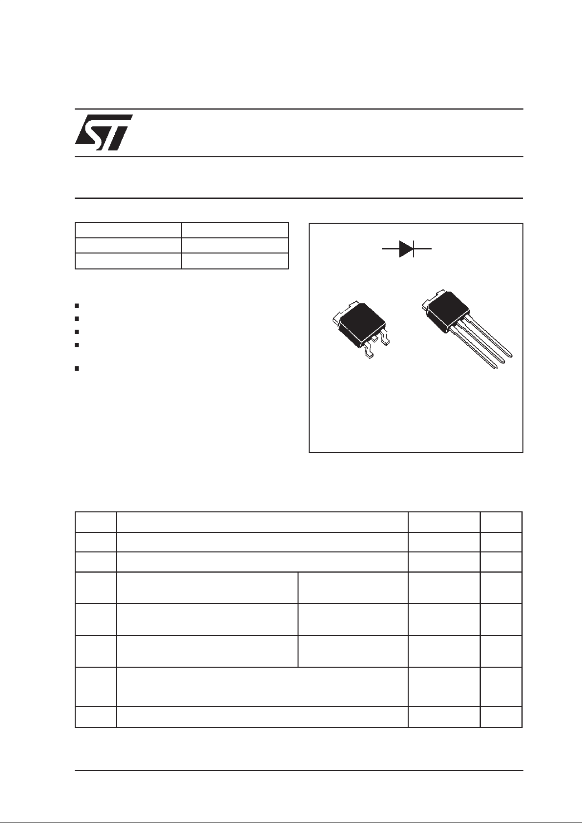
DESCRIPTION
DPAK
STPS360B
4
1
2
3
Symbol Parameter Value Unit
V
RRM
Repetitivepeakreversevoltage 60 V
I
F(RMS)
RMSforwardcurrent 6 A
I
F(AV)
Averageforwardcurrent Tcase= 140°C
δ =0.5
3A
I
FSM
Surgenonrepetitiveforwardcurrent tp = 10ms
Sinusoidal
50 A
I
RRM
Repetitivepeak
reversecurrent
tp = 2µs
F = 1kHz
1A
T
stg
Storagetemperaturerange - 65 to +150 °C
Tj Maximumjunctiontemperature 150
dV/dt Criticalrate of rise ofreversevoltage 10000 V/µs
ABSOLUTERATINGS (limitingvalue)
2
4(TAB)
3
1
2
3
4
IPAK
STPS360B-1
1/5
Page 2
Symbol Parameter Value Unit
R
th(j-c)
Junctionto case 3.5
°
C/W
THERMAL RESISTANCES
Symbol Tests Conditions TestsConditions Min. Typ. Max. Unit
I
R
* Reverseleakage current Tj = 25°CV
R
=60V 30
µ
A
Tj = 125°C 3 10 mA
V
F
** Forwardvoltage drop Tj = 25°CI
F
= 3 A 0.65 V
Tj = 125°CI
F
= 3 A 0.55 0.59
STATICELECTRICALCHARACTERISTICS
Pulse test : * tp = 380 µs, δ <2%
** tp = 5ms, δ <2%
To evaluate the maximum conduction losses usethe following equation :
P = 0.49 xI
F(AV)
+ 0.035 I
F2(RMS)
Typical junction capacitance, VR= 0V F =1MHz Tj= 25°C C=700pF
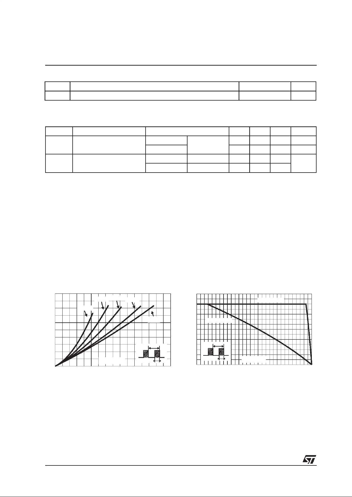
0.0 0.5 1.0 1.5 2.0 2.5 3.0 3.5 4.0
0.0
0.5
1.0
1.5
2.0
2.5
IF(av) (A)
PF(av)(W)
T
δ
=tp/T
tp
δ = 0.5
δ =0.2
δ = 0.1
δ = 0.05
δ =1
Fig. 1:
Averageforwardpower dissipationversus
averageforwardcurrent.
0 25 50 75 100 125 150
0.0
0.5
1.0
1.5
2.0
2.5
3.0
3.5
Tamb(°C)
IF(av)(A)
Rth(j-a)=65°C/W
Rth(j-a)=Rth(j-c)
T
δ
=tp/T
tp
Fig. 2:
Average forward current versus ambient
temperature(δ=0.5).
STPS360B(-TR)/B-1
2/5
Page 3

0 5 10 15 20 25 30 35 40 45 50 55 60
1E-7
1E-6
1E-5
1E-4
1E-3
1E-2
VR(V)
IR(A)
Tj=125°C
Tj=75°C
Tj=25°C
Tj=100°C
Fig. 5: Reverse leakage current versus reverse
voltageapplied (typicalvalues).
1 2 5 10 20 50 100
10
20
50
100
200
500
VR(V)
C(pF)
F=1MHz
Tj=25°C
Fig. 6:
Junction capacitance versus reverse volt-
age applied (typicalvalues).
0.0 0.2 0.4 0.6 0.8 1.0 1.2 1.4 1.6 1.8 2.0
0.1
1.0
10.0
50.0
VFM(V)
IFM(A)
Tj=125°C
Tj=25°C
Fig. 7: Forward voltage drop versus forward current(maximum values).
02468101214161820
0
20
40
60
80
100
S(Cu)
(cm )
Rth(j-a) (°C/W)
Fig.8: Thermalresistancejunctiontoambientver-
suscoppersurfaceundertab (Epoxyprinted circuit
boardFR4, copperthickness:35µm).
1E-3 1E-2 1E-1 1E+0
0
2
4
6
8
10
12
14
16
t(s)
IM(A)
Ta=25°C
Ta=50°C
Ta=100°C
IM
t
δ=0.5
Fig. 3:
Non repetitive surge peak forward current
versusoverloadduration (maximumvalues).
1E-3 1E-2 1E-1 1E+0
0.0
0.1
0.2
0.3
0.4
0.5
0.6
0.7
0.8
0.9
1.0
tp(s)
Zth(j-c)/Rth(j-c)
T
δ
=tp/T
tp
Single pulse
δ = 0.5
δ = 0.2
δ = 0.1
Fig. 4:
Relative variation of thermal impedance
junctionto caseversuspulseduration.
STPS360B(-TR)/B-1
3/5
Page 4

PACKAGEMECHANICAL DATA
IPAK
H
L
L1
G
B5
B
V1
D
C
A1
A3
A
C2
B3
B6
L2
E
B2
REF.
DIMENSIONS
Millimeters Inches
Min. Typ. Max. Min. Typ. Max.
A 2.2 2.4 0.086 0.094
A1 0.9 1.1 0.035 0.043
A3 0.7 1.3 0.027 0.051
B 0.64 0.9 0.025 0.035
B2 5.2 5.4 0.204 0.212
B3 0.85 0.033
B5 0.3 0.035
B6 0.95 0.037
C 0.45 0.6 0.017 0.023
C2 0.48 0.6 0.019 0.023
D 6 6.2 0.236 0.244
E 6.4 6.6 0.252 0.260
G 4.4 4.6 0.173 0.181
H 15.9 16.3 0.626 0.641
L 9 9.4 0.354 0.370
L1 0.8 1.2 0.031 0.047
L2 0.8 1 0.031 0.039
V1 10° 10°
STPS360B(-TR)/B-1
4/5
Page 5

REF.
DIMENSIONS
Millimeters Inches
Min. Typ. Max Min. Typ. Max.
A 2.20 2.40 0.086 0.094
A1 0.90 1.10 0.035 0.043
A2 0.03 0.23 0.001 0.009
B 0.64 0.90 0.025 0.035
B2 5.20 5.40 0.204 0.212
C 0.45 0.60 0.017 0.023
C2 0.48 0.60 0.018 0.023
D 6.00 6.20 0.236 0.244
E 6.40 6.60 0.251 0.259
G 4.40 4.60 0.173 0.181
H 9.35 10.10 0.368 0.397
L2 0.80 0.031
L4 0.60 1.00 0.023 0.039
V2 0° 8° 0° 8°
PACKAGEMECHANICAL DATA
DPAK
Informationfurnished isbelieved to beaccurate and reliable.However, STMicroelectronics assumes noresponsIbilityfor theconsequences of
use ofsuch informationnor forany infringementof patents or otherrights of thirdparties which may result from itsuse. Nolicense isgrantedby
implication or otherwise under any patent or patent rights of STMicroelectronics. Specifications mentioned in this publication are subject to
change withoutnotice. This publication supersedes andreplaces all information previously supplied.
STMicroelectronics products are not authorized for use as critical components in life support devices or systems without express written approval ofSTMicroelectronics.
The ST logo is aregisteredtrademark of STMicroelectronics
1998 STMicroelectronics - Printedin Italy- All rights reserved.
STMicroelectronicsGROUP OF COMPANIES
Australia - Brazil - Canada - China - France - Germany - Italy - Japan - Korea - Malaysia - Malta - Mexico - Morocco -
The Netherlands Singapore - Spain - Sweden - Switzerland - Taiwan - Thailand - United Kingdom - U.S.A.
6.7
6.7
6.7
3
1.61.6
2.32.3
FOOT PRINT DIMENSIONS
(in millimeters)
STPS360B(-TR)/B-1
5/5
 Loading...