

Page 1
STPS30U100DJF
ULVF™ power Schottky rectifier
Features
■ High current capability
■ Ultralow forward voltage drop
■ Low thermal resistance
■ High frequency operation
■ High integration
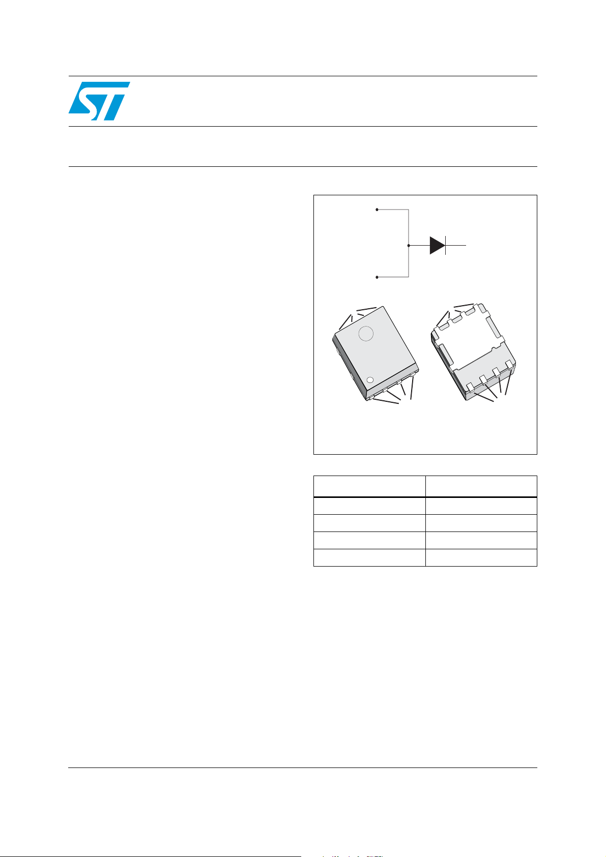
Description
The STPS30U100DJF is a power Schottky
rectifier featuring an ultralow forward voltage drop
(ULVF), suited for high frequency switch mode
power supply and DC to DC converters.
Packaged in PowerFLAT™, this device is
intended to be used in notebook, game station
and desktop adapters, providing these
applications with good efficiency at both low and
high load. Its low profile was especially designed
to be used in applications with space-saving
constraints.
A
A
K
A
PowerFLAT 5x6
STPS30U100DJF
Table 1. Device summary
Symbol Value
K
K
A
I
F(AV)
V
RRM
(max) 150 °C
T
j
V
(typ) 0.69 V
F
TM: ULVF and PowerFLAT are trademarks of
STMicroelectronics
30 A
100 V
May 2011 Doc ID 18121 Rev 3 1/8
www.st.com
8
Page 2
Characteristics STPS30U100DJF
1 Characteristics
Table 2. Absolute ratings (limiting values, anode terminals short circuited)
Symbol Parameter Value Unit
V
I
F(RMS)
I
F(AV)
I
T
1. condition to avoid thermal runaway for a diode on its own heatsink
Table 3. Thermal resistance
Symbol Parameter Value Unit
Repetitive peak reverse voltage 100 V
RRM
Forward rms current 45 A
Average forward current Tc = 75°C, δ = 0.5 30 A
Surge non repetitive forward current tp = 10 ms sine-wave 200 A
FSM
Storage temperature range -65 to + 150 °C
stg
Maximum operating junction temperature
T
j
dPtot
dTj
<
Rth(j-a)
1
(1)
150 °C
R
Table 4. Static electrical characteristics (anode terminals short circuited)
Junction to case 2.5 °C/W
th(j-c)
Symbol Parameter Test conditions Min. Typ. Max. Unit
= 125 °C VR = 70 V - 8 - mA
T
j
(1)
I
V
Reverse leakage current
R
(2)
Forward voltage drop
F
T
= 25 °C
j
= 125 °C - 20 45 mA
T
j
= 125 °C IF = 5 A - 0.38 0.42
T
j
T
= 125 °C IF = 10 A - 0.475 0.53
j
= 25 °C
T
j
Tj = 125 °C - 0.69 0.77
VR = V
= 30 A
I
F
RRM
--170µA
- - 0.855
1. Pulse test: tp = 5 ms, δ < 2%
2. Pulse test: tp = 380 µs, δ < 2%
To evaluate the maximum conduction losses use the following equation:
P = 0.590 x I
+ 0.006 x I
F(AV)
F2(RMS)
V
2/8 Doc ID 18121 Rev 3
Page 3
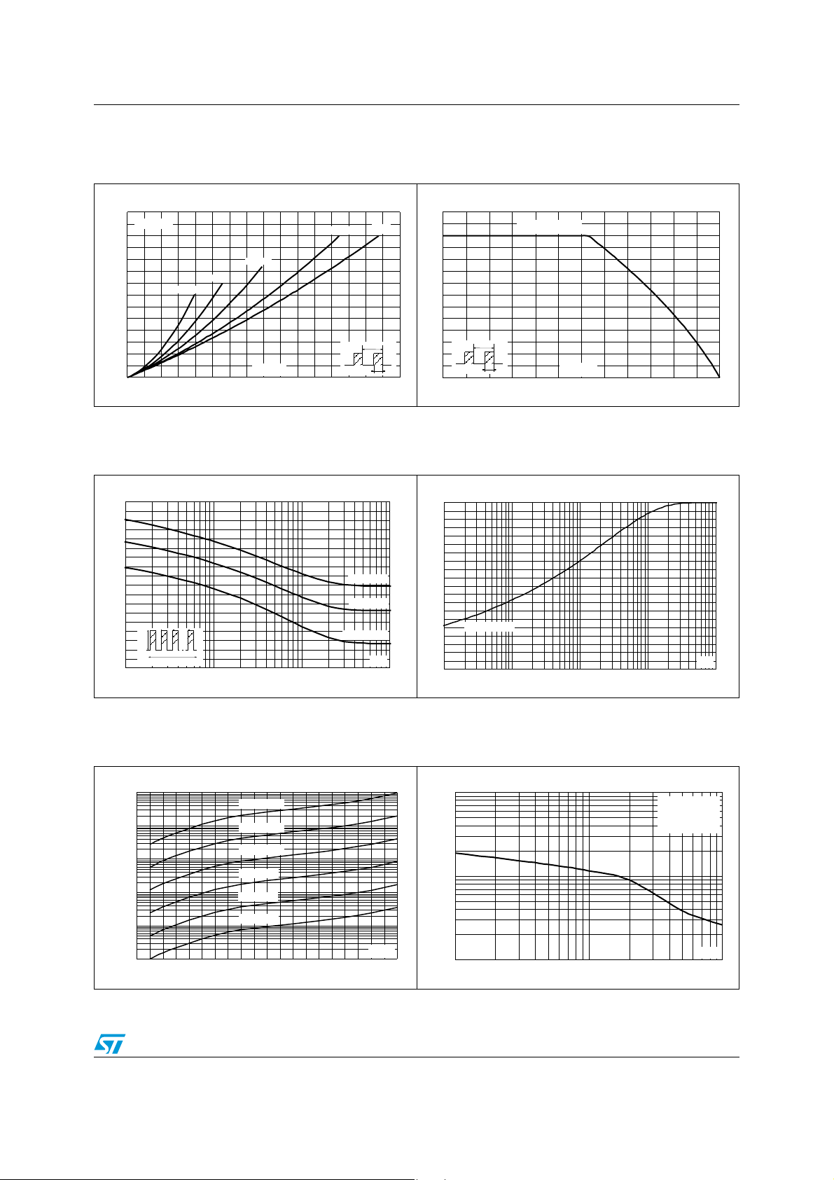
STPS30U100DJF Characteristics
Figure 1. Average forward power dissipation
versus average forward current
(maximum values)
P (W)
F(AV)
35.0
T = 75 °C
30.0
25.0
20.0
c
δ = 0.5
δ = 0.2
δ = 0.1
δ = 0.05
δ = 1
15.0
10.0
δ = t / T
p
T
t
p
5.0
0.0
I (A)
F(AV)
0 5 10 15 20 25 30 35 40
Figure 3. Non repetitive surge peak forward
current versus overload duration
(maximum values)
I (A)
M
180
160
140
120
100
80
60
40
I
M
20
0
δ = 0.5
t
1.E-03 1.E-02 1.E-01 1.E+00
T = 25 °C
c
T = 75 °C
c
T = 125 °C
c
t(s)
Figure 2. Average forward current versus
ambient temperature (δ = 0.5)
I (A)
F(AV)
35
30
R
th th
(j-a)
= R
(j-c)
25
20
15
10
δ = t / T
p
T
t
p
T (°C)
amb
5
0
0 25 50 75 100 125 150
Figure 4. Relative variation of thermal
impedance, junction to case,
versus pulse duration
Z/R
th(j-c) th(j-c)
1.0
0.9
0.8
0.7
0.6
0.5
0.4
0.3
Single pulse
0.2
0.1
0.0
1.E-04 1.E-03 1.E-02 1.E-01 1.E+00
t (s)
p
Figure 5. Reverse leakage current versus
reverse voltage applied
(typical values)
I (mA)
R
1.E+02
1.E+01
1.E+00
1.E-01
1.E-02
1.E-03
0 10 2030405060708090100
T = 150 °C
j
T = 125 °C
j
T = 100 °C
j
T = 75 °C
j
T = 50 °C
j
T = 25 °C
j
Figure 6. Junction capacitance versus
reverse voltage applied
(typical values)
C(pF)
10000
1000
V (V)
R
100
1 10 100
Doc ID 18121 Rev 3 3/8
F = 1 MHz
V = 30 mV
osc RMS
T = 25 °C
j
V (V)
R
Page 4

Characteristics STPS30U100DJF
Figure 7. Forward voltage drop versus
forward current
I (A)
FM
1.E+02
1.E+01
1.E+00
1.E-01
1.E-02
0.0 0.1 0.2 0.3 0.4 0.5 0.6 0.7 0.8 0.9 1.0 1.1 1.2
T = 125 °C
j
(Maximum values)
T = 125 °C
j
(Typical values)
T = 25 °C
j
(Maximum values)
V (V)
FM
Figure 8. Thermal resistance, junction to
ambient, versus copper surface
under tab
R (°C/W)
th(j-a)
250
200
150
100
50
0
012345678910
Epoxy printed circuit board FR4,
copper thickness = 35 µm
S (cm²)
cu
4/8 Doc ID 18121 Rev 3
Page 5

STPS30U100DJF Application information
2 Application information
It is mandatory to ensure a peak reverse voltage below the V
absolute rating. Therefore
RRM
ST recommends the use of an RC clamping snubber circuit in parallel with the
STPS30U100DJF device.
Figure 9. Application schematic
R
DC/DC input
STPS30U100DJF
C
DC/DC output
Doc ID 18121 Rev 3 5/8
Page 6

Package information STPS30U100DJF
3 Package information
● Epoxy meets UL94,V0
● Lead-free package
In order to meet environmental requirements, ST offers these devices in different grades of
ECOPACK
specifications, grade definitions and product status are available at: www.st.com
ECOPACK
Table 5. PowerFLAT 5x6 dimensions
®
packages, depending on their level of environmental compliance. ECOPACK®
®
is an ST trademark.
.
Dimensions
Ref.
D2
E2
K
b
e
A
A1
D
L
A2
A 0.80 1.00 0.031 0.039
A1 0.02 0.05 0.001 0.002
A2 0.25 0.010
b 0.30 0.50 0.012 0.020
D 5.20 0.205
Millimeters Inches
Min. Typ. Max. Min. Typ. Max.
D2 4.11 4.31 0.162 0.170
e 1.27 0.050
E
E 6.15 0.242
E2 3.50 3.70 0.138 0.146
L 0.50 0.80 0.020 0.031
Figure 10. Footprint (dimensions in mm)
6/8 Doc ID 18121 Rev 3
K 1.275 1.575 0.050 0.062
5.35
4.41
4.33
3.86
6.29
0.98
0.95
1.27
0.62
Page 7

STPS30U100DJF Ordering information
Figure 11. Tape and reel specifications
Dot identifying Pin A1 location
2.0
4.0
Ø 1.55
0.30
12.0
5.30
1.20
All dimensions are typical values in mm
4 Ordering information
0.20
6.30
8.0
User direction of unreeling
1.75
Ø 1.5
5.5
R 0.50
Table 6. Ordering information
Order code Marking Package Weight Base qty Delivery mode
STPS30U100DJF-TR PS30 U100 PowerFLAT 5x6 95 mg 3000 Tape and reel
5 Revision history
Table 7. Document revision history
Date Revision Changes
02-Nov-2010 1 First issue.
09-Dec-2010 2
20-May-2011 3
Added “maximum” to conduction loss calculation in
Section 1 on page 2.
Added reference E in Ta bl e 5 . Updated package graphics.
Updated base quantity and marking in Ta b le 6 . Added
Figure 11.
Doc ID 18121 Rev 3 7/8
Page 8

STPS30U100DJF
Please Read Carefully:
Information in this document is provided solely in connection with ST products. STMicroelectronics NV and its subsidiaries (“ST”) reserve the
right to make changes, corrections, modifications or improvements, to this document, and the products and services described herein at any
time, without notice.
All ST products are sold pursuant to ST’s terms and conditions of sale.
Purchasers are solely responsible for the choice, selection and use of the ST products and services described herein, and ST assumes no
liability whatsoever relating to the choice, selection or use of the ST products and services described herein.
No license, express or implied, by estoppel or otherwise, to any intellectual property rights is granted under this document. If any part of this
document refers to any third party products or services it shall not be deemed a license grant by ST for the use of such third party products
or services, or any intellectual property contained therein or considered as a warranty covering the use in any manner whatsoever of such
third party products or services or any intellectual property contained therein.
UNLESS OTHERWISE SET FORTH IN ST’S TERMS AND CONDITIONS OF SALE ST DISCLAIMS ANY EXPRESS OR IMPLIED
WARRANTY WITH RESPECT TO THE USE AND/OR SALE OF ST PRODUCTS INCLUDING WITHOUT LIMITATION IMPLIED
WARRANTIES OF MERCHANTABILITY, FITNESS FOR A PARTICULAR PURPOSE (AND THEIR EQUIVALENTS UNDER THE LAWS
OF ANY JURISDICTION), OR INFRINGEMENT OF ANY PATENT, COPYRIGHT OR OTHER INTELLECTUAL PROPERTY RIGHT.
UNLESS EXPRESSLY APPROVED IN WRITING BY AN AUTHORIZED ST REPRESENTATIVE, ST PRODUCTS ARE NOT
RECOMMENDED, AUTHORIZED OR WARRANTED FOR USE IN MILITARY, AIR CRAFT, SPACE, LIFE SAVING, OR LIFE SUSTAINING
APPLICATIONS, NOR IN PRODUCTS OR SYSTEMS WHERE FAILURE OR MALFUNCTION MAY RESULT IN PERSONAL INJURY,
DEATH, OR SEVERE PROPERTY OR ENVIRONMENTAL DAMAGE. ST PRODUCTS WHICH ARE NOT SPECIFIED AS "AUTOMOTIVE
GRADE" MAY ONLY BE USED IN AUTOMOTIVE APPLICATIONS AT USER’S OWN RISK.
Resale of ST products with provisions different from the statements and/or technical features set forth in this document shall immediately void
any warranty granted by ST for the ST product or service described herein and shall not create or extend in any manner whatsoever, any
liability of ST.
ST and the ST logo are trademarks or registered trademarks of ST in various countries.
Information in this document supersedes and replaces all information previously supplied.
The ST logo is a registered trademark of STMicroelectronics. All other names are the property of their respective owners.
© 2011 STMicroelectronics - All rights reserved
Australia - Belgium - Brazil - Canada - China - Czech Republic - Finland - France - Germany - Hong Kong - India - Israel - Italy - Japan -
STMicroelectronics group of companies
Malaysia - Malta - Morocco - Philippines - Singapore - Spain - Sweden - Switzerland - United Kingdom - United States of America
www.st.com
8/8 Doc ID 18121 Rev 3
 Loading...