

Page 1
®
MAIN PRODUCT CHARACTERISTICS
STPS1L60/A
POWER SCHOTTKY RECTIFIER
I
F(AV)
V
RRM
1A
60 V
Tj (max) 150°C
(max) 0.56 V
V
F
FEATURES AND BENEFITS
NEGLIGIBLE SWITCHING LOSSES
■
LOW FORWARD VOLTAGE DROP
■
AVALANCHE CAPABILITY SPECIFIED
■
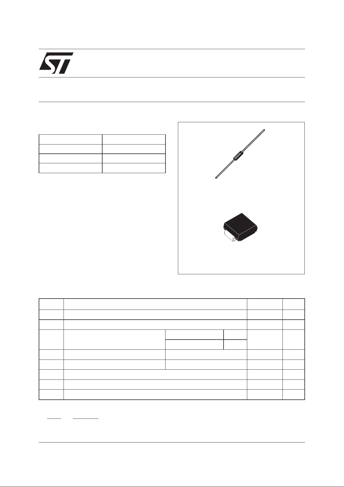
DO-41
STPS1L60
DESCRIPTION
Axial and Surface Mount Power Schottky rectifier
suited for Switch Mode Power Supplies and high
frequency DC to DC converters. Packaged in
SMA
STPS1L60A
DO-41 and SMA, this device is intended for use in
low voltage, high frequency inverters and small
battery chargers.
ABSOLUTE RATINGS (limiting values)
Symbol Parameter Value Unit
V
RRM
I
F(RMS)
I
F(AV)
Repetitive peak reverse voltage
RMS forward current
Average forward current TL= 130°C δ = 0.5 SMA
60 V
10 A
1A
I
*:
FSM
P
ARM
T
T
dV/dt
dPtot
Surge non repetitive forward current tp = 10 ms Sinusoidal
Repetitive peak avalanche power tp = 1µs Tj = 25°C
stg
Storage temperature range
j
Maximum junction temperature *
Critical rate of rise of reverse voltage
<
dTj Rth j a
July 2003 - Ed: 5A
T
= 120°C δ = 0.5 DO-41
L
thermal runaway condition for a diode on its ownheatsink
−1()
40 A
1200 W
- 65 to + 150 °C
150 °C
10000 V/µs
1/6
Page 2
STPS1L60/A
THERMAL RESISTANCES
Symbol Parameter Value Unit
R
th(j-a)
Junction to ambient Lead length = 10 mm DO-41
SMA
R
th(j-l)
Junction to leads Lead length = 10 mm DO-41
SMA
STATIC ELECTRICAL CHARACTERISTICS
Symbol Parameter Tests conditions Min. Typ. Max. Unit
*
I
R
V
F
Pulse test : * tp = 380 µs, δ <2%
Reverse leakage current Tj= 25°C VR= 60V
T
= 100°C
j
*
Forward voltage drop Tj= 25°C IF=1A
T
= 100°C
j
T
= 125°C
j
T
= 25°C IF=2A
j
T
= 100°C
j
T
= 125°C
j
100 °C/W
120
45
30
50 µA
1.5 5 mA
0.57 V
0.56
0.5 0.54
0.75
0.68
0.6 0.66
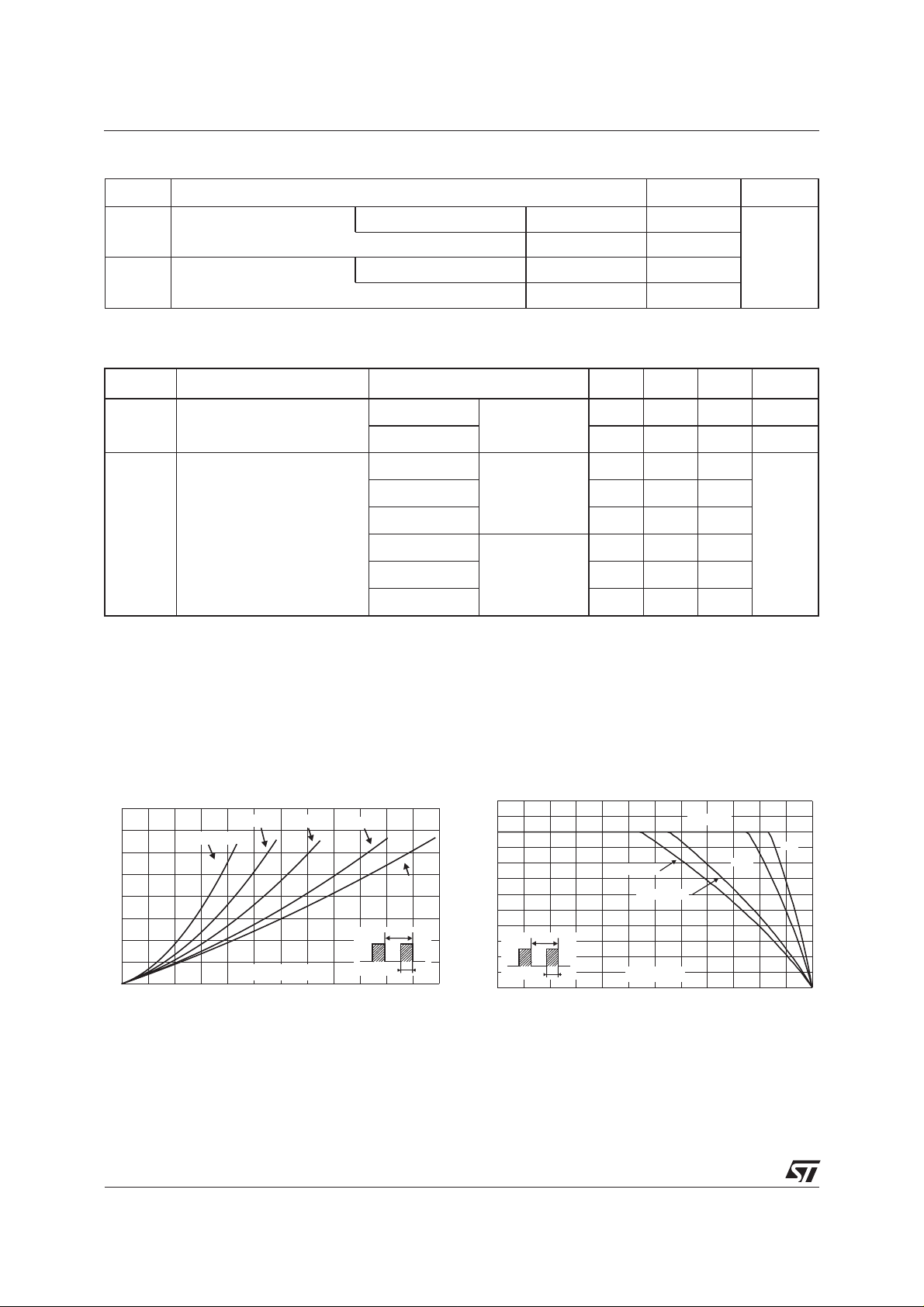
To evaluate the maximum conduction losses use the following equation:
P=0.44xI
Fig. 1: Average forward power dissipation versus
average forward current.
P (W)
F(AV)
0.8
0.6
0.4
0.2
0.0
0.0 0.2 0.4 0.6 0.8 1.0 1.2
F(AV)
δ = 0.05
+0.12xI
δ = 0.1
I (A)
F(AV)
F2(RMS)
δ = 0.2
δ = 0.5
δ
=tp/T
δ = 1
T
Fig. 2: Average forward current versus ambient
temperature (δ = 0.5).
I (A)
F(AV)
1.2
1.0
0.8
0.6
0.4
0.2
tp
0.0
0 25 50 75 100 125 150
δ
=tp/T
T
tp
R =120°C/W
th(j-a)
R =100°C/W
th(j-a)
T (°C)
amb
R=R
th(j-a) th(j-I)
SMA
DO-41
2/6
Page 3

STPS1L60/A
Fig. 3: Normalized avalanche power derating
versus pulse duration.
P(t)
ARM p
P (1µs)
ARM
1
0.1
0.01
t (µs)
0.001
0.10.01 1
p
10 100 1000
Fig.5-1:Non repetitive surgepeakforwardcurrent
versus overload duration (maximum values)
(DO-41).
I (A)
M
8
7
6
T =25°C
5
4
3
2
IM
1
0
1.E-03 1.E-02 1.E-01 1.E+00
δ=0.5
t
t(s)
a
T =50°C
a
T =100°C
a
Fig. 4: Normalized avalanche power derating
versus junction temperature.
P(t)
ARM p
P (25°C)
ARM
1.2
1
0.8
0.6
0.4
0.2
T (°C)
0
j
0 25 50 75 100 125 150
Fig.5-2:Non repetitive surgepeakforwardcurrent
versus overload duration (maximum values)
(SMA).
I (A)
M
8
7
6
5
4
3
2
IM
1
0
1.E-03 1.E-02 1.E-01 1.E+00
δ=0.5
t
t(s)
T =25°C
a
T =50°C
a
T =100°C
a
Fig. 6-1: Relative variation of thermal impedance
junctiontoambient versus pulseduration(DO-41).
Z/R
th(j-a) th(j-a)
1.0
0.9
0.8
0.7
0.6
δ = 0.5
0.5
0.4
0.3
δ = 0.2
0.2
δ = 0.1
0.1
0.0
1.E-01 1.E+00 1.E+01 1.E+02 1.E+03
Single pulse
t (s)
p
δ
=tp/T
T
tp
Fig. 6-2: Relative variation of thermal impedance
junction to ambient versus pulse duration (SMA).
Z/R
th(j-a) th(j-a)
1.0
0.9
0.8
0.7
0.6
δ = 0.5
0.5
0.4
0.3
δ = 0.2
0.2
δ = 0.1
0.1
Single pulse
0.0
1.E-02 1.E-01 1.E+00 1.E+01 1.E+02
t (s)
p
δ
=tp/T
T
tp
3/6
Page 4

STPS1L60/A
Fig. 7: Reverse leakage current versus reverse
voltage applied (typical values).
I (mA)
R
1E+1
1E+0
1E-1
1E-2
1E-3
1E-4
0 5 10 15 20 25 30 35 40 45 50 55 60
T=125°C
j
T=100°C
j
T=25°C
j
V (V)
R
Fig. 9-1: Forward voltage drop versus forward
current (low level, maximum values) (DO-41).
I (A)
FM
2.0
1.8
1.6
1.4
1.2
1.0
0.8
0.6
0.4
0.2
0.0
0.0 0.1 0.2 0.3 0.4 0.5 0.6 0.7 0.8 0.9 1.0
T=100°C
j
V (V)
FM
T=25°C
j
Fig. 8: Junction capacitance versus reverse
voltage applied (typical values).
C(pF)
200
F=1MHz
T=25°C
j
100
50
20
V (V)
10
1 10 100
R
Fig. 9-2: Forward voltage drop versus forward
current (high level, maximum values) (SMA).
I (A)
FM
10
T=100°C
j
5
2
1
0.0 0.2 0.4 0.6 0.8 1.0 1.2 1.4 1.6 1.8 2.0 2.2 2.4 2.6
V (V)
FM
T=25°C
j
Fig. 10: Thermal resistance junction to ambient
versus copper surface under each lead (Epoxy
printed circuit board FR4, Cu: 35µm) (SMA).
R (°C/W)
th(j-)
140
120
100
80
60
40
20
0
012345
4/6
S(Cu)(cm²)
Fig. 11: Thermal resistance versus lead length
(DO-41).
R (°C/W)
th
120
R
100
80
60
40
20
0
5 10152025
th(j-a)
R
th(j-I)
L (mm)
leads
Page 5

PACKAGE MECHANICAL DATA
SMA (JEDEC DO-214AC)
E1
REF.
STPS1L60/A
DIMENSIONS
Millimeters Inches
Min. Max. Min. Max.
D
E
A1
C
L
A2
FOOT PRINT DIMENSIONS (in millimeters)
1.65
1.45 1.45
2.40
A1 1.90 2.70 0.075 0.106
A2 0.05 0.20 0.002 0.008
b 1.25 1.65 0.049 0.065
c 0.15 0.41 0.006 0.016
E 4.80 5.60 0.189 0.220
E1 3.95 4.60 0.156 0.181
b
D 2.25 2.95 0.089 0.116
5/6
Page 6

STPS1L60/A
PACKAGE MECHANICAL DATA
DO-41 plastic
CA
O
/
D
C
O
/
D
BO
/
DIMENSIONS
REF.
Millimeters Inches
Min. Max. Min. Max.
A 4.07 5.20 0.160 0.205
B 2.04 2.71 0.080 0.107
C 28 1.102
Ordering type Marking Package Weight Base qty Delivery mode
STPS1L60 Partnumber
DO-41 0.34g 2000 Ammopack
cathode ring
STPS1L60RL Partnumber
DO-41 0.34g 5000 Tape & Reel
cathode ring
STPS1L60A GB6 SMA 0.068 g 5000 Tape & Reel
■
EPOXY MEETS UL94,V0
Informationfurnished is believedto be accurateand reliable. However,STMicroelectronics assumes noresponsibility for theconsequences of
useof suchinformationnor forany infringement ofpatents or otherrights of thirdparties which mayresult from itsuse. No licenseis grantedby
implication or otherwise under any patent or patent rights of STMicroelectronics. Specifications mentioned in this publication are subject to
change withoutnotice. This publication supersedes and replaces all information previously supplied.
STMicroelectronics products are not authorized for use as critical components in life support devices or systems without express written
approval ofSTMicroelectronics.
The ST logo is a registered trademark of STMicroelectronics
© 2003 STMicroelectronics - Printed in Italy - All rights reserved.
STMicroelectronics GROUP OF COMPANIES
Australia - Brazil - Canada - China - Finland - France - Germany
Hong Kong - India - Israel - Italy - Japan - Malaysia - Malta - Morocco - Singapore
Spain - Sweden - Switzerland - United Kingdom - United States.
http://www.st.com
6/6
 Loading...