

Page 1
®
LOW DROP POWER SCHOTTKY RECTIFIER
MAIN PRODUCT CHARACTERISTICS
STPS1L30M
I
F(AV)
V
RRM
1A
30 V
Tj (max) 150°C
V
(max) 0.38V
F
FEATURES AND BENEFITS
VERY SMALL CONDUCTION LOSSES
■
NEGLIGIBLE SWITCHING LOSSES
■
EXTREMELY FAST SWITCHING
■
LOW FORWARD VOLTAGE DROP FOR
■
HIGHER EFFICIENCY & EXTENDED
BATTERY LIFE
LOW THERMAL RESISTANCE
■
AVALANCHE CAPABILITY SPECIFIED
■
DESCRIPTION
Single Schottky rectifier suited for switch mode
power supplies and high frequency DC to DC
converters.
Packaged in ST Mite, this device is intended for
use in low voltage, high frequency inverters, free
wheeling and polarity protection applications. Due
to the small size of the package this device fits
battery powered equipment (cellular, notebook,
PDA’s, printers) as well chargers and PCMCIA
cards.
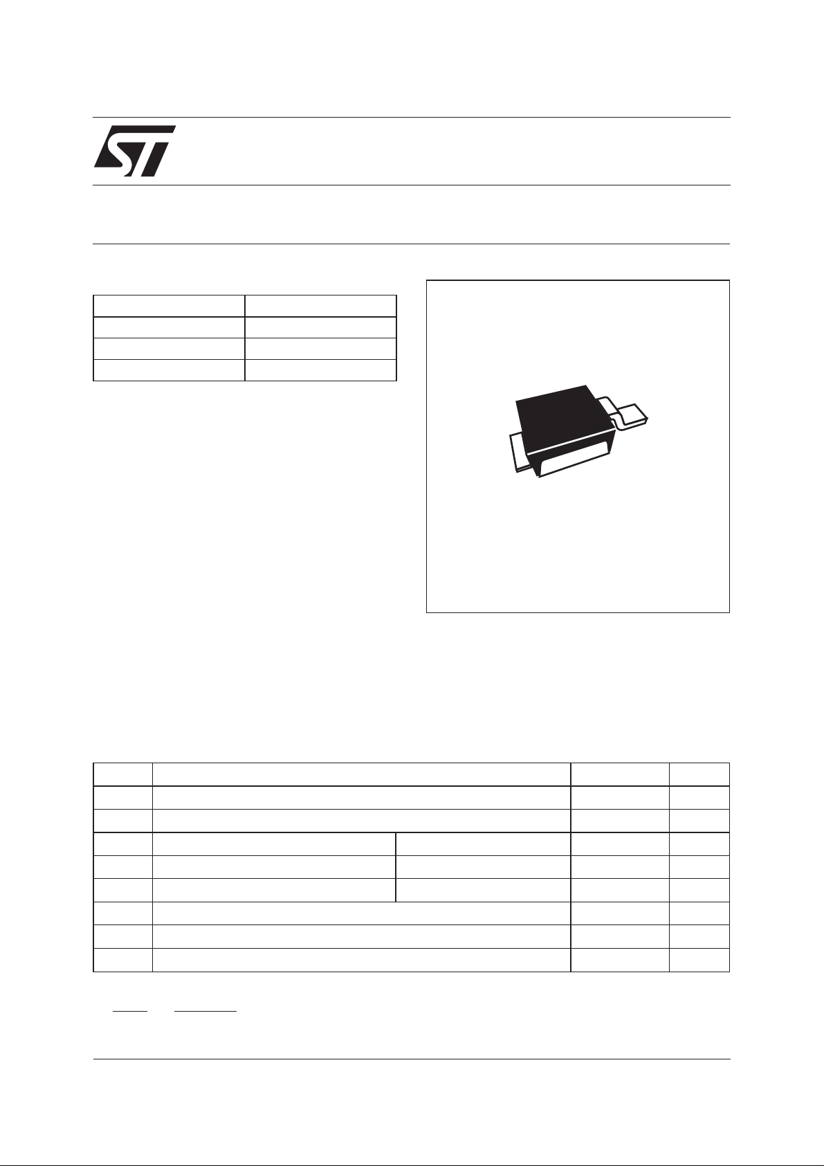
A
C
ST Mite
(DO-216AA)
ABSOLUTE RATINGS (limiting values)
Symbol Parameter Value Unit
V
RRM
I
F(RMS)
I
F(AV)
I
FSM
P
ARM
T
Repetitive peak reverse voltage 30 V
RMS forward current 2 A
Average forward current Tc = 140°C δ = 0.5 1 A
Surge non repetitive forward current tp = 10 ms sinusoidal 50 A
Repetitive peak avalanche power tp = 1µs Tj = 25°C 1200 W
Storage temperature range - 65 to + 150 °C
stg
Tj Maximum operating junction temperature* 150 °C
dV/dt Critical rate of rise of reverse voltage (rated Vr, Tj = 25°C) 10000 V/µs
dPtot
*:
<
dTj Rth j a
July 2003 - Ed : 2A
thermal runaway condition for a diode on its own heatsink
−1()
1/5
Page 2
STPS1L30M
THERMAL RESISTANCE
Symbol Parameter Value Unit
R
R
th (j-c)
th (j-a)
Junction to case 20 °C/W
Junction to ambient with minimum recommended pad size,
PC board FR4
STATIC ELECTRICAL CHARACTERISTICS
Value
Symbol Parameter Tests conditions
Min. Typ. Max.
I
* Reverse leakage current Tj = 25°C VR=V
R
RRM
0.13 0.39 mA
Tj = 85°C 5.25 16.5
Tj = 25°C V
= 20 V 0.05 0.24
R
Tj = 85°C 3.5 10.5
Tj = 25°C V
= 10 V 0.03 0.15
R
Tj = 85°C 2.4 7
V
* Forward voltage drop Tj= 25°C IF= 1A 0.33 0.39 V
F
Tj = 85°C 0.28 0.34
250 °C/W
Unit
Tj = 25°C I
= 3 A 0.45 0.53
F
Tj=85°C 0.43 0.51
Pulse test : * tp ≤ 380 µs, δ≤2%
To evaluate the conduction losses use the following equation :
P=0.34xI
F(AV)
+ 0.07 I
F2(RMS)
2/5
Page 3

STPS1L30M
Fig.1:Conductionlossesversus average current.
P (W)F(AV)
0.50
0.45
0.40
0.35
0.30
0.25
0.20
0.15
0.10
0.05
0.00
0.0 0.1 0.2 0.3 0.4 0.5 0.6 0.7 0.8 0.9 1.0 1.1 1.2 1.3
δ = 0.05
δ = 0.1
I (A)F(AV)
δ = 0.2
δ = 0.5
δ
=tp/T
δ = 1
T
tp
Fig. 3: Normalized avalanche power derating
versus pulse duration.
P(t)
ARM p
P (1µs)
ARM
1
0.1
0.01
t (µs)
0.001
0.10.01 1
p
10 100 1000
Fig. 2: Average forward current versus ambient
temperature (δ = 0.5)
I (A)F(AV)
1.1
1.0
0.9
0.8
0.7
0.6
0.5
0.4
0.3
0.2
0.1
0.0
0 25 50 75 100 125 150
R
th(j-a)
=270°C/W
T (°C)amb
R
th(j-a)=Rth(j-c)
Fig. 4: Normalized avalanche power derating
versus junction temperature.
P(t)
ARM p
P (25°C)
ARM
1.2
1
0.8
0.6
0.4
0.2
0
0 25 50 75 100 125 150
T (°C)
j
Fig. 5: Non repetitive surge peak forward current
versus overload duration (maximum values).
I (A)M
22
20
18
16
14
12
10
8
6
IM
4
2
0
1.E-03 1.E-02 1.E-01 1.E+00
δ=0.5
t
t(s)
TC=25°C
TC=75°C
TC=125°C
Fig. 6: Relative variation of thermal impedance
junction to case versus pulse duration.
Zth(j-c)/Rth(j-c)
1.0
0.9
0.8
0.7
0.6
δ = 0.5
0.5
0.4
0.3
δ = 0.2
0.2
δ = 0.1
0.1
Single pulse
0.0
1.E-04 1.E-03 1.E-02 1.E-01
t (s)P
δ
=tp/T
T
tp
3/5
Page 4

STPS1L30M
Fig. 7: Reverse leakage current versus reverse
voltage applied (typical values).
I (mA)R
1.E+03
Tj=150°C
1.E+02
1.E+01
1.E+00
1.E-01
1.E-02
024681012141618202224262830
Tj=125°C
Tj=100°C
Tj=75°C
Tj=50°C
Tj=25°C
V (V)R
Fig. 9: Junction capacitance versus reverse
voltage applied (typical values).
C(pF)
1000
100
V (V)R
10
1 10 100
F=1MHz
V
osc
T
=30mV
=25°C
j
Fig. 8: Reverse leakage current versus junction
temperature (typical values).
I (mA)R
1.E+03
1.E+02
1.E+01
1.E+00
1.E-01
VR=30V
Tj(°C)
1.E-02
0 25 50 75 100 125 150
Fig. 10: Forward voltage drop versus forward
current.
I (A)FM
2.0
1.8
1.6
1.4
1.2
1.0
0.8
0.6
0.4
0.2
0.0
0.00 0.05 0.10 0.15 0.20 0.25 0.30 0.35 0.40 0.45 0.50
Tj=85°C
Tj=85°C
(Maximum values)
(Maximum values)
Tj=85°C
Tj=85°C
(Typical values)
(Typical values)
V (V)FM
Tj=25°C
(Maximum values)
Fig. 11: Thermal resistance junction to ambient
versus copper surface under tab (epoxy printed
board FR4, Cu = 35µm, typical values).
th(j-a)
R (°C/W)
250
200
150
100
50
S(mm²)
0
0 20 40 60 80 100 120 140 160 180 200
4/5
Page 5

PACKAGE MECHANICAL DATA
ST Mite
L3
b2
C
D
b
H
L2
L
R
R1
A1
0° to 6°
STPS1L30M
DIMENSIONS
REF.
A 0.85 1.00 1.15 0.033 0.039 0.045
A1 0.10 0.004
b 0.40 0.65 0.016 0.025
b2 0.70 1.00 0.027 0.039
c 0.10 0.25 0.004 0.010
D 1.75 1.90 2.05 0.069 0.075 0.081
E
E 1.75 1.90 2.05 0.069 0.075 0.081
H 3.60 3.75 3.90 0.142 0.148 0.154
A
L 0.50 0.63 0.80 0.047 0.025 0.031
L2 1.20 1.35 1.50 0.047 0.053 0.059
L3 0.50 ref (Typ.) 0.019 ref (Typ.)
R 0.07 0.003
R1 0.07 0.003
Millimeters Inches
Min. Typ. Max. Min. Typ. Max.
Note: The anode is connected to the longer tab
The cathode is connected to the shorter tab (heatsink)
FOOTPRINT (dimensions in mm)
2.67
0.762
2.54
0.635
1.27
Type Marking Package Weight Base qty Delivery mode
STPS1L30M 1L3 ST Mite 15.5 mg 12000 Tape & reel
Informationfurnished is believed to be accurate and reliable.However, STMicroelectronics assumes no responsibility for the consequencesof
useof such information nor for any infringementof patents or other rights of third partieswhich may result from its use. Nolicense is granted by
implication or otherwise under any patent or patent rights of STMicroelectronics. Specifications mentioned in this publication are subject to
change without notice. This publication supersedes and replaces all information previously supplied.
STMicroelectronics products are not authorized for use as critical components in life support devices or systems without express written
approval of STMicroelectronics.
The ST logo is a registered trademark of STMicroelectronics
© 2003 STMicroelectronics - Printed in Italy - All rights reserved.
STMicroelectronics GROUP OF COMPANIES
Australia - Brazil - Canada - China - Finland - France - Germany
Hong Kong - India - Israel - Italy - Japan - Malaysia - Malta - Morocco - Singapore
Spain - Sweden - Switzerland - United Kingdom - United States.
http://www.st.com
5/5
 Loading...