

Page 1
®
LOW DROP POWER SCHOTTKY RECTIFIER
MAIN PRODUCTS CHARACTERISTICS
I
F(AV)
V
RRM
Tj (max) 150 °C
V
(max) 0.45 V
F
FEATURES AND BENEFITS
LOW FORWARD VOLTAGE DROP MEANING
■
VERY SMALL CONDUCTION LOSSES
LOW SWITCHING LOSSES ALLOWING HIGH
■
FREQUENCY OPERATION
INSULATED PACKAGE: TO-220FPAB
■
Insulated voltage: 2000V DC
Capacitance: 12 pF
AVALANCHE CAPABILITY SPECIFIED
■
DESCRIPTION
Dual center tap Schottky barrier rectifier designed
for highfrequencySwitchedModePowerSupplies
and high frequency DC to DC converters.
Packaged in TO-220AB and TO-220FPAB, these
devices are intended for use in low voltage, high
frequency converters, free-wheeling and polarity
protection applications.
ABSOLUTE RATINGS (limiting values, per diode)
2x8A
45 V
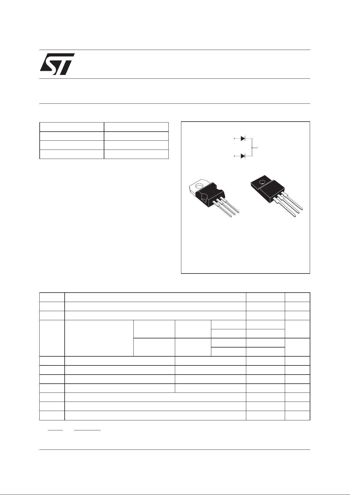
STPS16L45CT/CFP
A1
K
A2
A2
K
A1
TO-220AB
STPS16L45CT
TO-220FPAB
STPS16L45CFP
A1
A2
K
Symbol Parameter Value Unit
V
RRM
I
F(RMS)
I
F(AV)
I
FSM
I
RRM
I
RSM
P
ARM
T
stg
Tj
dV/dt
dPtot
*:
Repetitive peak reverse voltage
RMS forward current
Average forward current
Surge non repetitive forward current tp = 10 ms sinusoidal
Repetitive peak reverse current tp=2 µs square F=1kHz
Non repetitive peak reverse current tp = 100 µs square
Repetitive peak avalanche power tp = 1µs Tj = 25°C
Storage temperature range
Maximum operating junction temperature *
Critical rate of rise of reverse voltage
<
dTj Rth j a
July 2003 - Ed : 3C
TO-220AB
TO-220FPAB
Tc = 140°C
δ = 0.5
Tc = 125°C
δ = 0.5
Per diode
Per device
Per diode
Per device
thermal runaway condition for a diodeon its own heatsink
−1()
45 V
30 A
8
16
8
16
180 A
1A
2A
4000 W
-65 to+150 °C
150 °C
10000 V/µs
A
A
1/5
Page 2
STPS16L45CT/CFP
THERMAL RESISTANCES
Symbol Parameter Value Unit
R
th(j-c)
Junction to case TO-220AB
TO-220FPAB
When the diodes 1 and 2 areused simultaneously :
∆ Tj(diode 1) = P(diode1) x R
(Per diode) + P(diode 2) x R
th(j-c)
STATIC ELECTRICAL CHARACTERISTICS (per diode)
Symbol Parameter Tests Conditions Min. Typ. Max. Unit
*
I
R
V
F
Reverse leakage
current
*
Forward voltage drop Tj = 25°CI
Tj = 25°C V
Tj = 125°C
Tj = 125°C I
Tj=25°CI
Tj = 125°C I
Pulse test : * tp = 380 µs, δ <2%
R=VRRM
=8A
F
=8A
F
=16A
F
=16A
F
Per diode
Total
Coupling
Per diode
Total
Coupling
th(c)
2.2
°C/W
1.3
0.3
4.5
3.5
2.5
0.2 mA
65 130 mA
0.5 V
0.39 0.45
0.63
0.55 0.64
To evaluate the conduction losses use the following equation :
P=0.26xI
Fig. 1: Average forward power dissipation versus
average forward current (per diode).
PF(av)(W)
6.0
5.5
5.0
4.5
4.0
3.5
3.0
2.5
2.0
1.5
1.0
0.5
0.0
012345678910
Fig. 3: Normalized avalanche power derating
versus pulse duration.
P(t)
ARM p
P (1µs)
ARM
1
0.1
0.01
0.001
+ 0.024 I
F(AV)
δ = 0.1
δ = 0.05
0.10.01 1
F2(RMS)
δ = 0.2
IF(av) (A)
t (µs)
p
δ = 0.5
δ = 1
T
=tp/T
δ
10 100 1000
tp
Fig. 2: Average current versus ambient
temperature (δ = 0.5) (per diode).
IF(av)(A)
9
8
7
6
5
4
3
2
1
=tp/T
δ
0
0 25 50 75 100 125 150
Fig. 4: Normalized avalanche power derating
versus junction temperature.
P(t)
ARM p
P (25°C)
ARM
1.2
1
0.8
0.6
0.4
0.2
0
0 25 50 75 100 125 150
Rth(j-a)=Rth(j-c)
Rth(j-a)=15°C/W
T
tp
Tamb(°C)
T (°C)
j
TO-220AB
TO-220FPAB
2/5
Page 3

STPS16L45CT/CFP
Fig. 5-1:Nonrepetitivesurgepeak forward current
versus overload duration (maximum values per
diode, TO-220AB).
IM(A)
120
100
80
60
40
IM
20
0
1E-3 1E-2 1E-1 1E+0
δ=0.5
t
t(s)
Tc=25°C
Tc=75°C
Tc=125°C
Fig. 6-1: Relative variation of thermal impedance
junction to case versus pulse duration
(TO-220AB).
Zth(j-c)/Rth(j-c)
1.0
Fig. 5-2: Non repetitive surgepeak forward current
versus overload duration (maximum values per
diode, TO-220FPAB).
IM(A)
100
90
80
70
60
Tc=25°C
50
40
30
IM
20
10
0
1E-3 1E-2 1E-1 1E+0
δ=0.5
t
t(s)
Tc=50°C
Tc=100°C
Fig. 6-2: Relative variation of thermal impedance
junction to case versus pulse duration
(TO-220FPAB).
Zth(j-c)/Rth(j-c)
1.0
0.8
δ = 0.5
0.6
0.4
δ = 0.2
δ = 0.1
0.2
0.0
Single pulse
tp(s)
1E-4 1E-3 1E-2 1E-1 1E+0
δ
=tp/T
T
tp
Fig. 7: Reverse leakage current versus reverse
voltage applied (typical values) (per diode).
IR(mA)
2E+2
1E+2
1E+1
1E+0
1E-1
1E-2
0 5 10 15 20 25 30 35 40 45
Tj=150°C
Tj=125°C
Tj=75°C
Tj=25°C
VR(V)
0.8
δ = 0.5
0.6
0.4
δ = 0.2
δ = 0.1
0.2
Single pulse
0.0
1E-3 1E-2 1E-1 1E+0 1E+1
tp(s)
δ
=tp/T
T
tp
Fig. 8: Junction capacitance versus reverse
voltage applied (typical values) (per diode).
C(pF)
2000
1000
500
200
VR(V)
100
12 51020 50
F=1MHz
Tj=25°C
3/5
Page 4

STPS16L45CT/CFP
Fig. 9: Forward voltage drop versus forward
current (maximum values) (per diode).
IFM(A)
100.0
10.0
Tj=125°C
Typical values
Tj=150°C
Tj=25°C
1.0
Tj=75°C
VFM(V)
0.1
0.0 0.2 0.4 0.6 0.8 1.0 1.2 1.4 1.6 1.8
PACKAGE MECHANICAL DATA
TO-220FPAB
A
H
L6
L2
L3
L5
L4
G1
G
F1
F2
F
B
Dia
D
REF. DIMENSIONS
Millimeters Inches
Min. Max. Min. Max.
A 4.4 4.6 0.173 0.181
B 2.5 2.7 0.098 0.106
D 2.5 2.75 0.098 0.108
E 0.45 0.70 0.018 0.027
F 0.75 1 0.030 0.039
F1 1.15 1.70 0.045 0.067
F2 1.15 1.70 0.045 0.067
L7
G 4.95 5.20 0.195 0.205
G1 2.4 2.7 0.094 0.106
H 10 10.4 0.393 0.409
L2 16 Typ. 0.63 Typ.
L3 28.6 30.6 1.126 1.205
L4 9.8 10.6 0.386 0.417
L5 2.9 3.6 0.114 0.142
E
L6 15.9 16.4 0.626 0.646
L7 9.00 9.30 0.354 0.366
Dia. 3.00 3.20 0.118 0.126
4/5
Page 5

STPS16L45CT/CFP
PACKAGE MECHANICAL DATA
TO-220AB
H2
Dia
L5
L6
L2
F2
F1
F
G1
G
L9
L4
DIMENSIONS
REF.
A
C
A 4.40 4.60 0.173 0.181
Millimeters Inches
Min. Max. Min. Max.
C 1.23 1.32 0.048 0.051
L7
D 2.40 2.72 0.094 0.107
E 0.49 0.70 0.019 0.027
F 0.61 0.88 0.024 0.034
F1 1.14 1.70 0.044 0.066
F2 1.14 1.70 0.044 0.066
D
G 4.95 5.15 0.194 0.202
G1 2.40 2.70 0.094 0.106
H2 10 10.40 0.393 0.409
L2 16.4 typ. 0.645typ.
L4 13 14 0.511 0.551
M
E
L5 2.65 2.95 0.104 0.116
L6 15.25 15.75 0.600 0.620
L7 6.20 6.60 0.244 0.259
L9 3.50 3.93 0.137 0.154
M 2.6 typ. 0.102 typ.
Diam. 3.75 3.85 0.147 0.151
Ordering type Marking Package Weight Base qty Delivery mode
STPS16L45CT STPS16L45CT TO-220AB 2g 50 Tube
STPS16L45CFP STPS16L45CFP TO-220FPAB 2g 50 Tube
■
Epoxy meets UL94,V0
■
Cooling method : C
■
Recommended torque value : 0.55 m.N
■
Maximum torque value : 0.70 m.N
Informationfurnished is believed to be accurate andreliable.However, STMicroelectronics assumes no responsibility for theconsequences of
useof such information nor for anyinfringement of patents or other rightsof third parties which may resultfrom its use. No license isgranted by
implication or otherwise under any patent or patent rights of STMicroelectronics. Specifications mentioned in this publication are subject to
change without notice. This publication supersedes and replaces all information previously supplied.
STMicroelectronics products are not authorized for use as critical components in life support devices or systems without express written
approval of STMicroelectronics.
The ST logo is a registered trademark of STMicroelectronics
© 2003 STMicroelectronics - Printed in Italy - All rights reserved.
STMicroelectronics GROUP OF COMPANIES
Australia - Brazil - Canada - China - Finland - France - Germany
Hong Kong - India - Israel - Italy - Japan - Malaysia - Malta - Morocco - Singapore
Spain - Sweden - Switzerland - United Kingdom - United States.
http://www.st.com
5/5
 Loading...