

Page 1
Features
STPS1045B-Y
Automotive power Schottky rectifier
■ Negligible switching losses
■ Low forward voltage drop
■ Low capacitance
■ High reverse avalanche surge capability
■ Avalanche specification
■ AEC-Q101 qualified
Description
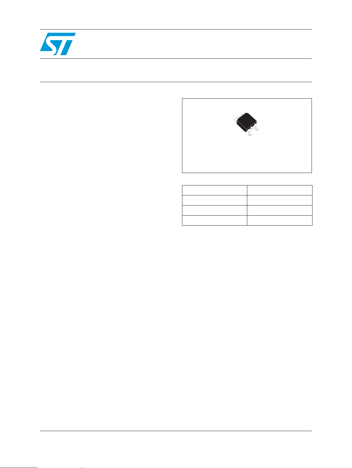
High voltage Schottky rectifier suited for switch
mode power supplies and other power converters.
Packaged in DPAK, this device is intended for use
in high frequency circuits where low switching
losses are required.
K
K
A
A
DPAK
STPS1045BY
j
Table 1. Device summary
I
F(AV)
V
RRM
T
j
V
(max) 0.57 V
F
10 A
45 V
175 °C
May 2011 Doc ID 17265 Rev 1 1/7
www.st.com
7
Page 2
Characteristics STPS1045B-Y
1 Characteristics
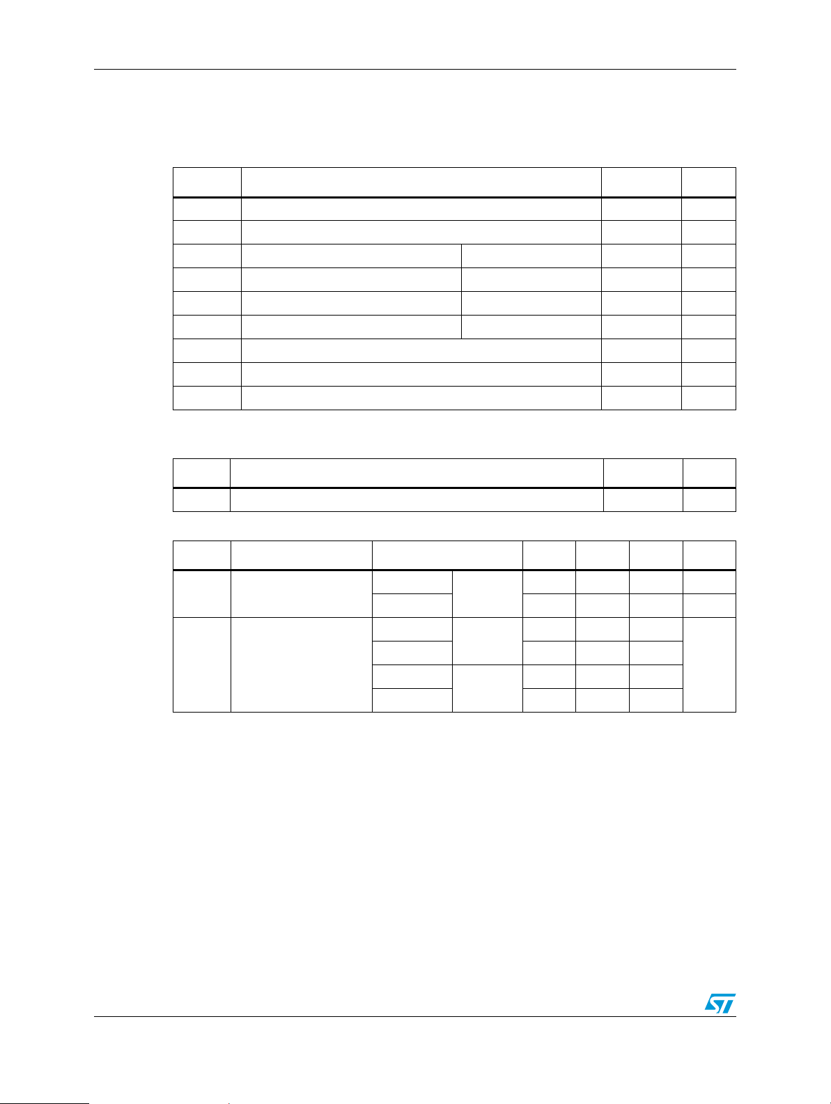
Table 2. Absolute maximum ratings
Symbol Parameter Value Unit
V
I
F(RMS)
I
F(AV)
I
I
P
T
RRM
FSM
RRM
ARM
T
Repetitive peak reverse voltage 45 V
/pin Forward rms current 7 A
Average forward current Tc = 150 °C δ = 0.5 10 A
Surge non repetitive forward current tp = 10 ms sinusoidal 75 A
Repetitive peak reverse current tp = 2 µs, F= 1 kHz 1 A
Repetitive peak avalanche power tp = 1 µs, T
Storage temperature range -65 to +175 °C
stg
Operating junction temperature range
j
(1)
25 °C 4000 W
j =
-40 to +175 °C
dV/dt Critical rate of rise of reverse voltage 10000 V/µs
dPtot
---------------
1. condition to avoid thermal runaway for a diode on its own heatsink
dTj
Table 3. Thermal parameters
1
------------------------- -
<
Rth j a–()
Symbol Parameter Value Unit
R
th(j-c)
Table 4. Static electrical characteristics
Junction to case 3 °C/W
Symbol Parameter Test conditions Min. Typ. Max. Unit
Reverse leakage
(1)
I
R
current
(2)
V
1. Pulse test: tp = 5 ms, δ < 2%
2. Pulse test: tp = 380 µs, δ < 2%
Forward voltage drop
F
= 25 °C
T
j
T
= 125 °C - 7 15 mA
j
= 25 °C
T
j
T
= 125 °C - 0.50 0.57
j
T
= 25 °C
j
= 125 °C - 0.65 0.72
T
j
= V
V
R
= 10 A
I
F
= 20 A
I
F
RRM
- - 100 μA
- - 0.63
- - 0.84
V
To evaluate the conduction losses use the following equation:
P = 0.42 x I
2/7 Doc ID 17265 Rev 1
F(AV)
+ 0.015 I
F2(RMS)
Page 3
STPS1045B-Y Characteristics
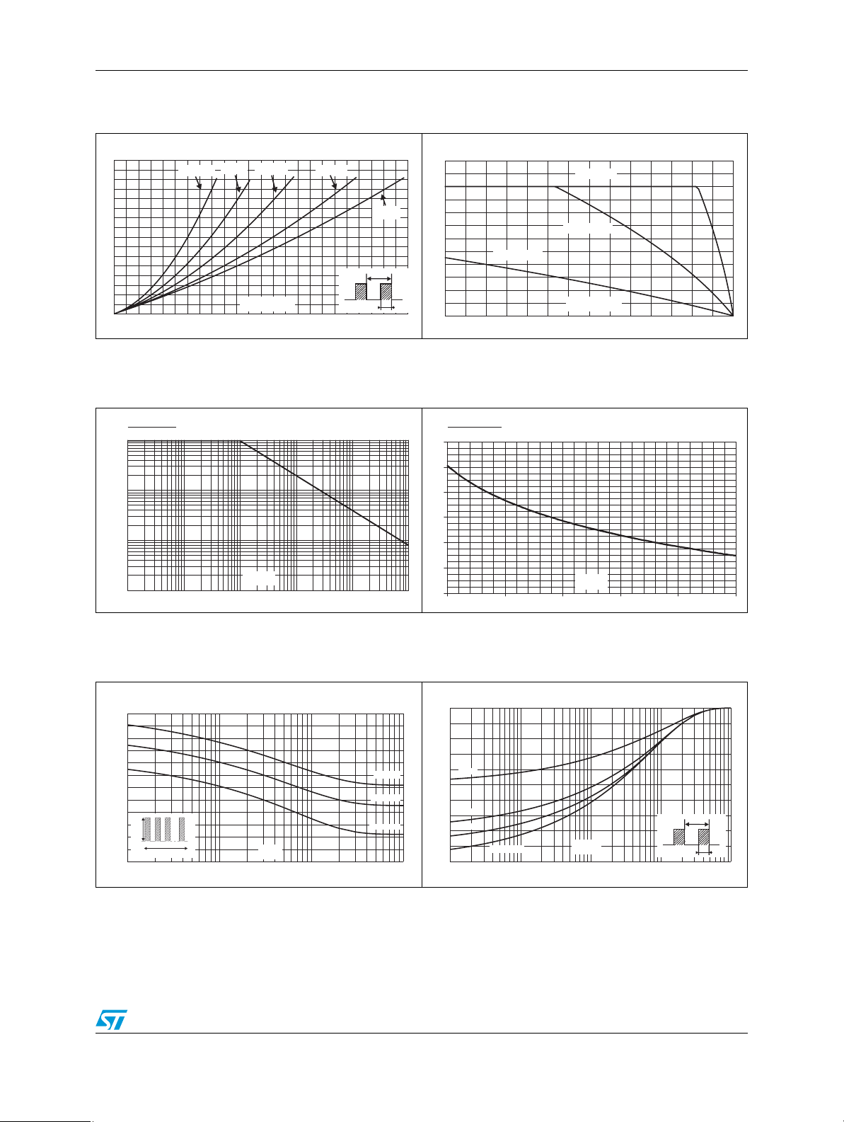
Figure 1. Average forward power dissipation
versus average forward current
P(W)
F(AV)
8
7
6
5
4
3
2
1
0
0123456789101112
δ = 0.05
δ = 0.1
δ = 0.2
I (A)
F(AV)
δ = 0.5
δ
=tp/T
δ = 1
T
tp
Figure 3. Normalized avalanche power
derating versus pulse duration
P(t)
ARM p
P (1µs)
ARM
1
0.1
Figure 2. Average forward current versus
ambient temperature (
I (A)
F(AV)
12
10
8
6
R =70°C/W
4
2
0
0 25 50 75 100 125 150 175
th(j-a)
R=R
th(j-a) th(j-c)
R =15°C/W
th(j-a)
T (°C)
amb
δ = 0.5)
Figure 4. Normalized avalanche power
derating versus junction
temperature
P(T)
ARM
P (25 °C)
1.2
1
0.8
j
ARM
0.01
t (µs)
0.001
0.10.01 1
p
10 100 1000
Figure 5. Non repetitive surge peak forward
current versus overload duration
(maximum values)
I (A)
M
120
100
80
60
40
IM
20
0
1E-3 1E-2 1E-1 1E+0
δ=0.5
t
t(s)
T =50°C
C
T =100°C
C
T =150°C
C
0.6
0.4
0.2
0
25 50 75 100 125 150
T (°C)
j
Figure 6. Relative variation of thermal
impedance junction to case versus
pulse duration
Z/R
th(j-c) th(j-c)
1.0
0.8
0.6
δ = 0.5
0.4
δ = 0.2
δ = 0.1
0.2
0.0
Single pulse
1E-4 1E-3 1E-2 1E-1 1E+0
t (s)
p
δ
T
=tp/T
tp
Doc ID 17265 Rev 1 3/7
Page 4
Characteristics STPS1045B-Y
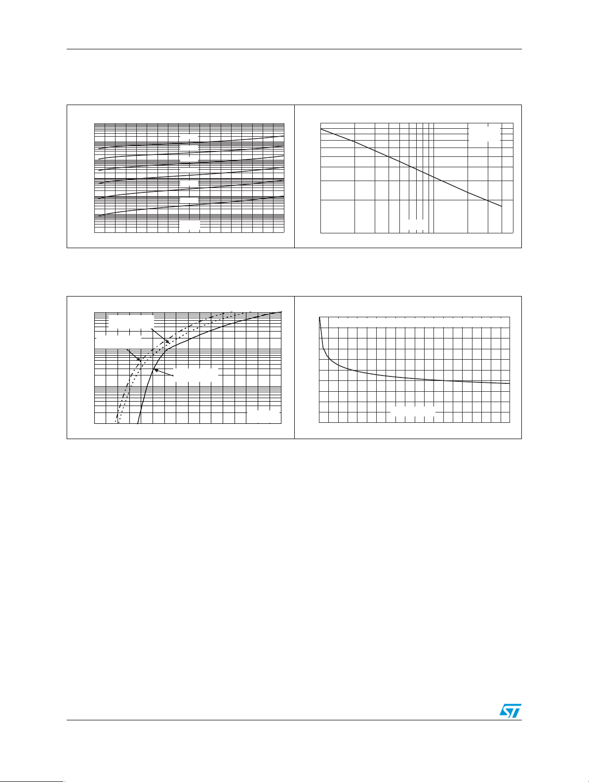
Figure 7. Reverse leakage current versus
reverse voltage applied
(typical values)
I (µA)
R
1E+5
T =150°C
1E+4
1E+3
1E+2
1E+1
1E+0
1E-1
0 5 10 15 20 25 30 35 40 45
j
T =125°C
j
T =100°C
j
T =75°C
j
T =50°C
j
T =25°C
j
V (V)
R
Figure 9. Forward voltage drop versus
forward current
I (A)
FM
100.0
10.0
1.0
0.1
T =125°C
j
(maximum values)
T =125°C
j
(typical values)
T =25°C
j
(maximum values)
V (V)
FM
0.0 0.2 0.4 0.6 0.8 1.0 1.2 1.4 1.6
Figure 8. Junction capacitance versus
reverse voltage applied
(typical values)
C(pF)
1000
500
200
V (V)
100
12 51020 50
R
F=1MHz
V =30mV
OSC RMS
T =25°C
j
Figure 10. Thermal resistance junction to
ambient versus copper surface
under tab
R
(°C/W)
th(j-a)
100
Epoxy printed circuit board, copper thickness: 35 µm
80
60
40
20
S(Cu)(cm )
0
0 2 4 6 8101214161820
2
4/7 Doc ID 17265 Rev 1
Page 5
STPS1045B-Y Package information
2 Package information
● Epoxy meets UL94, V0
● Lead-free package
In order to meet environmental requirements, ST offers these devices in different grades of
ECOPACK
specifications, grade definitions and product status are available at: www.st.com
ECOPACK
®
packages, depending on their level of environmental compliance. ECOPACK®
®
is an ST trademark.
.
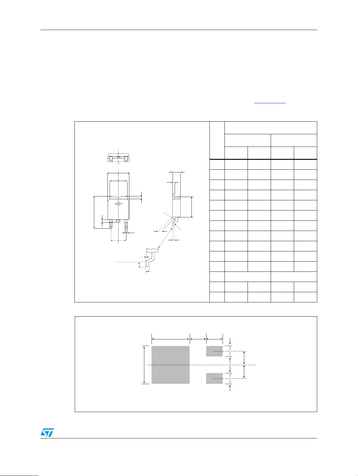
Table 5. DPAK dimensions
Dimensions
Ref.
A 2.20 2.40 0.086 0.094
E
B2
L2
A
C2
A1 0.90 1.10 0.035 0.043
A2 0.03 0.23 0.001 0.009
B 0.64 0.90 0.025 0.035
H
L4
B
G
R
A1
D
R
C
B2 5.20 5.40 0.204 0.212
C 0.45 0.60 0.017 0.023
C2 0.48 0.60 0.018 0.023
D 6.00 6.20 0.236 0.244
E 6.40 6.60 0.251 0.259
0.60 MIN.
A2
G 4.40 4.60 0.173 0.181
H 9.35 10.10 0.368 0.397
V2
L2 0.80 typ. 0.031 typ.
Millimeters Inches
Min. Max Min. Max.
Figure 11. DPAK footprint (dimensions in mm)
6.7 3 3
6.7
Doc ID 17265 Rev 1 5/7
L4 0.60 1.00 0.023 0.039
V2 0° 8° 0° 8°
1.6
2.3
2.3
1.6
Page 6
Ordering information STPS1045B-Y
3 Ordering information
Table 6. Ordering information
Order code Marking Package Weight Base qty Delivery mode
STPS1045BY-TR S1045Y DPAK 0.30 g 2500 Tape and reel
4 Revision history
Table 7. Document revision history
Date Revision Changes
23-May-2011 1 Initial release.
6/7 Doc ID 17265 Rev 1
Page 7

STPS1045B-Y
Please Read Carefully:
Information in this document is provided solely in connection with ST products. STMicroelectronics NV and its subsidiaries (“ST”) reserve the
right to make changes, corrections, modifications or improvements, to this document, and the products and services described herein at any
time, without notice.
All ST products are sold pursuant to ST’s terms and conditions of sale.
Purchasers are solely responsible for the choice, selection and use of the ST products and services described herein, and ST assumes no
liability whatsoever relating to the choice, selection or use of the ST products and services described herein.
No license, express or implied, by estoppel or otherwise, to any intellectual property rights is granted under this document. If any part of this
document refers to any third party products or services it shall not be deemed a license grant by ST for the use of such third party products
or services, or any intellectual property contained therein or considered as a warranty covering the use in any manner whatsoever of such
third party products or services or any intellectual property contained therein.
UNLESS OTHERWISE SET FORTH IN ST’S TERMS AND CONDITIONS OF SALE ST DISCLAIMS ANY EXPRESS OR IMPLIED
WARRANTY WITH RESPECT TO THE USE AND/OR SALE OF ST PRODUCTS INCLUDING WITHOUT LIMITATION IMPLIED
WARRANTIES OF MERCHANTABILITY, FITNESS FOR A PARTICULAR PURPOSE (AND THEIR EQUIVALENTS UNDER THE LAWS
OF ANY JURISDICTION), OR INFRINGEMENT OF ANY PATENT, COPYRIGHT OR OTHER INTELLECTUAL PROPERTY RIGHT.
UNLESS EXPRESSLY APPROVED IN WRITING BY AN AUTHORIZED ST REPRESENTATIVE, ST PRODUCTS ARE NOT
RECOMMENDED, AUTHORIZED OR WARRANTED FOR USE IN MILITARY, AIR CRAFT, SPACE, LIFE SAVING, OR LIFE SUSTAINING
APPLICATIONS, NOR IN PRODUCTS OR SYSTEMS WHERE FAILURE OR MALFUNCTION MAY RESULT IN PERSONAL INJURY,
DEATH, OR SEVERE PROPERTY OR ENVIRONMENTAL DAMAGE. ST PRODUCTS WHICH ARE NOT SPECIFIED AS "AUTOMOTIVE
GRADE" MAY ONLY BE USED IN AUTOMOTIVE APPLICATIONS AT USER’S OWN RISK.
Resale of ST products with provisions different from the statements and/or technical features set forth in this document shall immediately void
any warranty granted by ST for the ST product or service described herein and shall not create or extend in any manner whatsoever, any
liability of ST.
ST and the ST logo are trademarks or registered trademarks of ST in various countries.
Information in this document supersedes and replaces all information previously supplied.
The ST logo is a registered trademark of STMicroelectronics. All other names are the property of their respective owners.
© 2011 STMicroelectronics - All rights reserved
STMicroelectronics group of companies
Australia - Belgium - Brazil - Canada - China - Czech Republic - Finland - France - Germany - Hong Kong - India - Israel - Italy - Japan -
Malaysia - Malta - Morocco - Philippines - Singapore - Spain - Sweden - Switzerland - United Kingdom - United States of America
www.st.com
Doc ID 17265 Rev 1 7/7
 Loading...