

Page 1
Features
STPIC6C595
Power logic 8-bit shift register
■ Low R
■ 30 mJ avalanche energy
■ Eight 100 mA DMOS outputs
■ 250 mA current limit capability
■ 33 V output clamp voltage
■ Device are cascadable
■ Low power consumption
DS(on)
: 4 Ω typ
Description
This STPIC6C595 is a monolithic, mediumvoltage, low current power 8-bit shift register
designed for use in systems that require relatively
moderate load power such as LEDs. The device
contains a built-in voltage clamp on the outputs
for inductive transient protection. Power driver
applications include relays, solenoids, and other
low-current or medium-voltage loads.
The device contains an 8-bit serial-in, parallel-out
shift register that feeds an 8-bit D-type storage
register. Data transfers through both the shift and
storage register clock (SRCK) and the register
clock (RCK
data out the serial output (SER OUT) port on the
rising edge of SRCK. The storage register
transfers data to the output buffer when shift
register clear (CLR) is high. When CLR
input shift register is cleared. When output enable
(G
) is held high, all data in the output buffer is
held low and all drain output are off. When G is
held low, data from the storage register is
transparent to the output buffer.
), respectively. The device transfers
is low, the
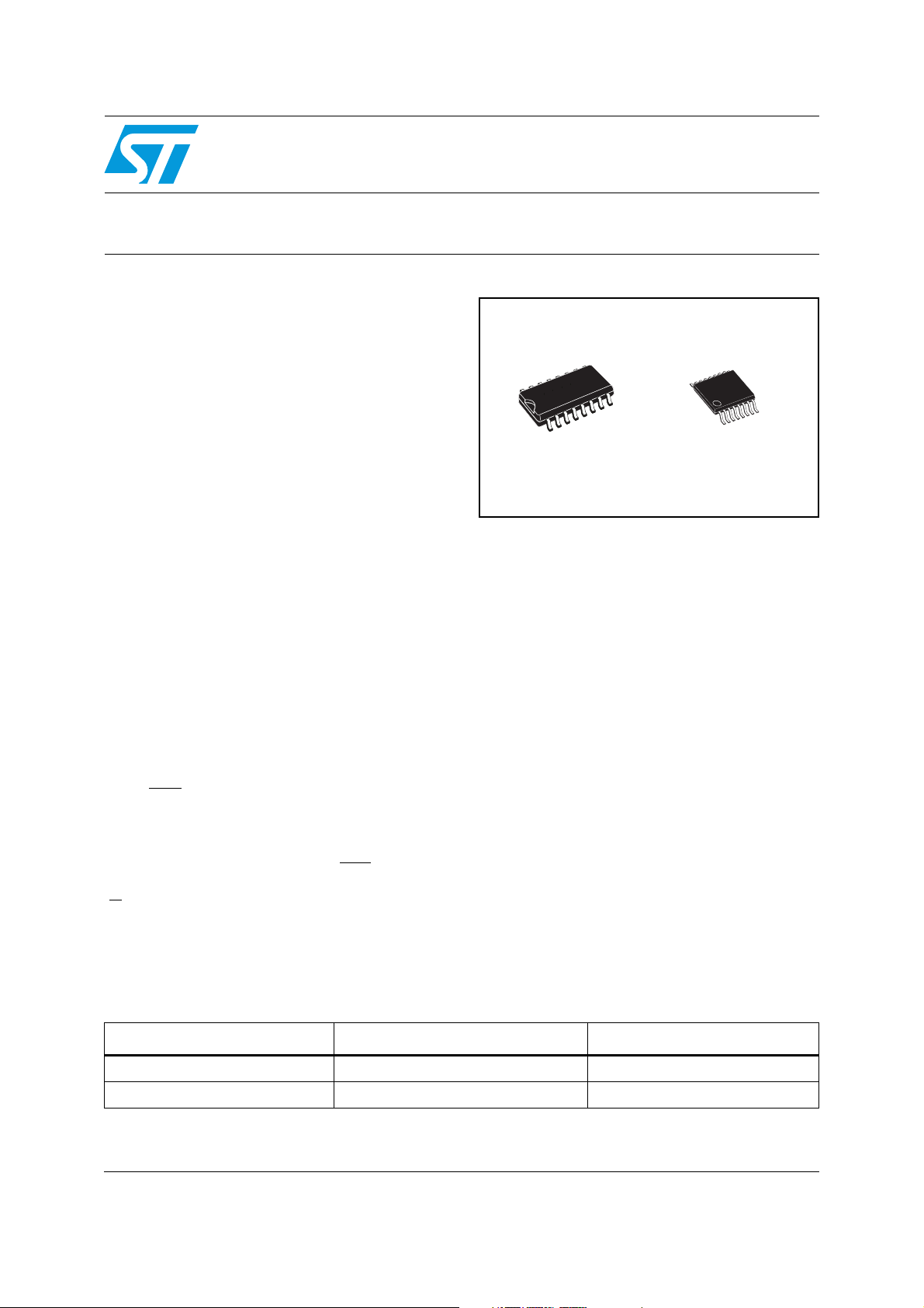
SO-16 TSSOP16
When data in the output buffers is low, the DMOS
transistor outputs are off. When data is high, the
DMOS transistor outputs have sink-current
capability. The SER OUT allows for cascading of
the data from the shift register to additional
devices.
Output are low-side, open-drain DMOS
transistors with output ratings of 33 V and 100 mA
continuous sink-current capability. Each output
provides a 250 mA maximum current limit at
T
= 25 °C. The current limit decreases as the
C
junction temperature increases for additional
device protection. The device also provides up to
1.5 kV of ESD protection when tested using the
human-body model and 150 V machine model.
The STPIC6C595 is characterized for operation
over the operating case temperature range of
-40 °C to 125 °C.
Table 1. Device summary
Order codes Package Packaging
STPIC6C595MTR SO-16 (Tape and reel) 2500 parts per reel
STPIC6C595TTR TSSOP16 (Tape and reel) 2500 parts per reel
March 2009 Rev 5 1/22
www.st.com
22
Page 2

Contents STPIC6C595
Contents
1 Logic symbol and pin configuration . . . . . . . . . . . . . . . . . . . . . . . . . . . . 3
2 Maximum rating . . . . . . . . . . . . . . . . . . . . . . . . . . . . . . . . . . . . . . . . . . . . . 4
2.1 Absolute maximum ratings . . . . . . . . . . . . . . . . . . . . . . . . . . . . . . . . . . . . . 4
2.2 Thermal data . . . . . . . . . . . . . . . . . . . . . . . . . . . . . . . . . . . . . . . . . . . . . . . 5
2.3 Recommended operating conditions . . . . . . . . . . . . . . . . . . . . . . . . . . . . . 5
3 Electrical characteristics . . . . . . . . . . . . . . . . . . . . . . . . . . . . . . . . . . . . . 6
3.1 DC characteristics . . . . . . . . . . . . . . . . . . . . . . . . . . . . . . . . . . . . . . . . . . . 6
3.2 Switching characteristics . . . . . . . . . . . . . . . . . . . . . . . . . . . . . . . . . . . . . . 7
4 Logic diagram . . . . . . . . . . . . . . . . . . . . . . . . . . . . . . . . . . . . . . . . . . . . . . 8
5 Typical operating circuit . . . . . . . . . . . . . . . . . . . . . . . . . . . . . . . . . . . . . . 9
6 Typical performance and characteristics . . . . . . . . . . . . . . . . . . . . . . . 13
7 Package mechanical data . . . . . . . . . . . . . . . . . . . . . . . . . . . . . . . . . . . . 16
8 Revision history . . . . . . . . . . . . . . . . . . . . . . . . . . . . . . . . . . . . . . . . . . . 21
2/22
Page 3
STPIC6C595 Logic symbol and pin configuration
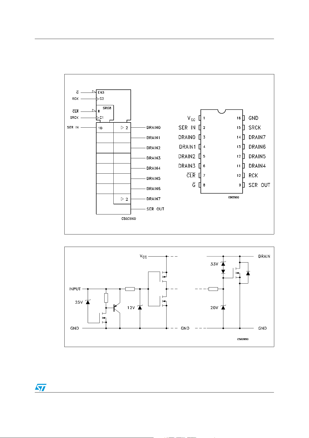
1 Logic symbol and pin configuration
Figure 1. Logic symbol and pin configuration
Figure 2. Input and output equivalent circuits
3/22
Page 4
Maximum rating STPIC6C595
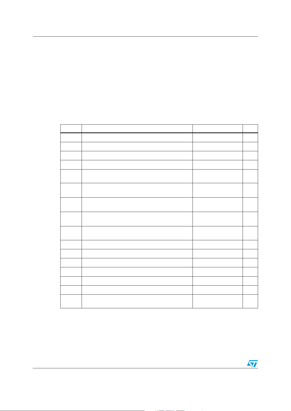
2 Maximum rating
Stressing the device above the rating listed in the “absolute maximum ratings” table may
cause permanent damage to the device. These are stress ratings only and operation of the
device at these or any other conditions above those indicated in the operating sections of
this specification is not implied. Exposure to absolute maximum rating conditions for
extended periods may affect device reliability.
2.1 Absolute maximum ratings
Table 2. Absolute maximum ratings
Symbol Parameter Value Unit
V
V
I
I
Logic supply voltage (See Note 1)7V
CC
V
Logic input voltage range -0.3 to 7 V
I
Power DMOS drain to source voltage (See Note 2)33V
DS
Continuous source to drain diode anode current 250 mA
DS
Pulsed source to drain diode anode current
DS
(See Note 3)
Pulsed drain current, each output, all output ON
I
D
I
D
I
D
= 25 °C)
(T
C
Continuous current, each output, all output ON
= 25 °C)
(T
C
Peak drain current single output
(TC = 25 °C) (See Note 3)
500 mA
250 mA
100 mA
250 mA
E
I
T
Single pulse avalanche energy
AS
(See Figure 11 and Figure 12)
Avalanche current (See Note 4 and Figure 17)200mA
AS
P
Continuous total dissipation (TC ≤ 25 °C)
d
P
Continuous total dissipation (TC = 125 °C)
d
T
Operating virtual junction temperature range -40 to +150 °C
J
T
Operating case temperature range -40 to +125 °C
C
Storage temperature range -65 to +150 °C
stg
Lead temperature 1.6 mm (1/16 inch) from case for 10
T
L
seconds
4/22
30 mJ
1087 mW
217 mW
260 °C
Page 5
STPIC6C595 Maximum rating
2.2 Thermal data
Table 3. Thermal data
Symbol Parameter Value Unit
R
th(JA)
Thermal resistance junction-ambient 115 °C/W
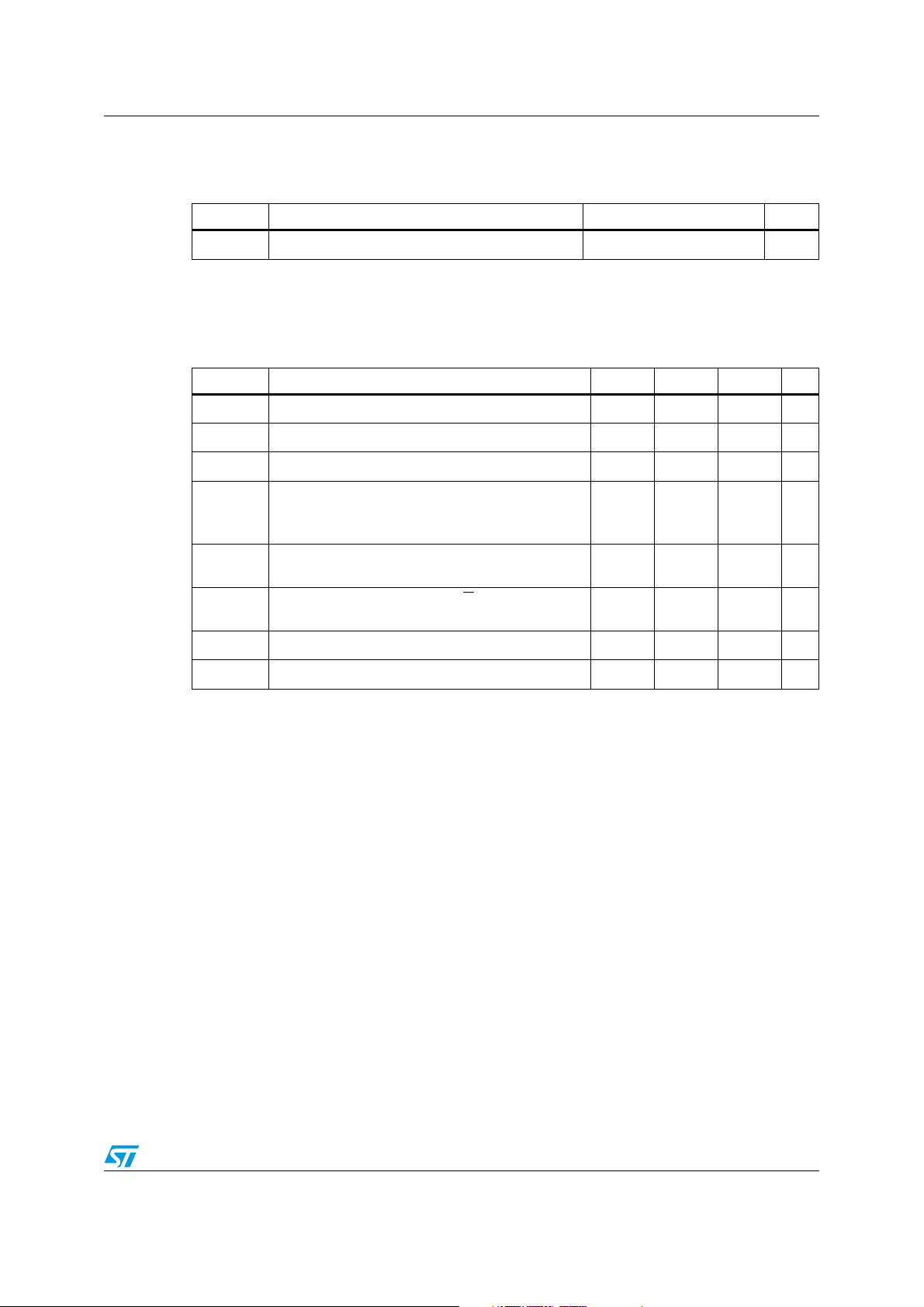
2.3 Recommended operating conditions
Table 4. Recommended operating conditions
Symbol Parameter Min Typ Max Unit
V
CC
V
V
I
DP
t
su
t
hL
Logic supply voltage 4.5 5.5 V
High level input voltage
IH
Low level input voltage 0
IL
0.85V
CC
Pulse drain output current
(TC = 25 °C, V
= 5 V, all outputs ON)
CC
(see Note 3, Note 5 and Figure 15)
Set-up time, SER IN high before SRCK ↑
(see Figure 4 and Figure 8)
Hold time, SER IN high before G ↑
(see Figure 4, Figure 7, Figure 8)
1.6 3.0 5.7 ns
2.8 4.0 9.6 ns
V
CC
0.15V
CC
250 mA
V
V
t
W
T
Pulse duration (see Figure 8)40ns
Operating case temperature -40 125 °C
C
5/22
Page 6
Electrical characteristics STPIC6C595
3 Electrical characteristics
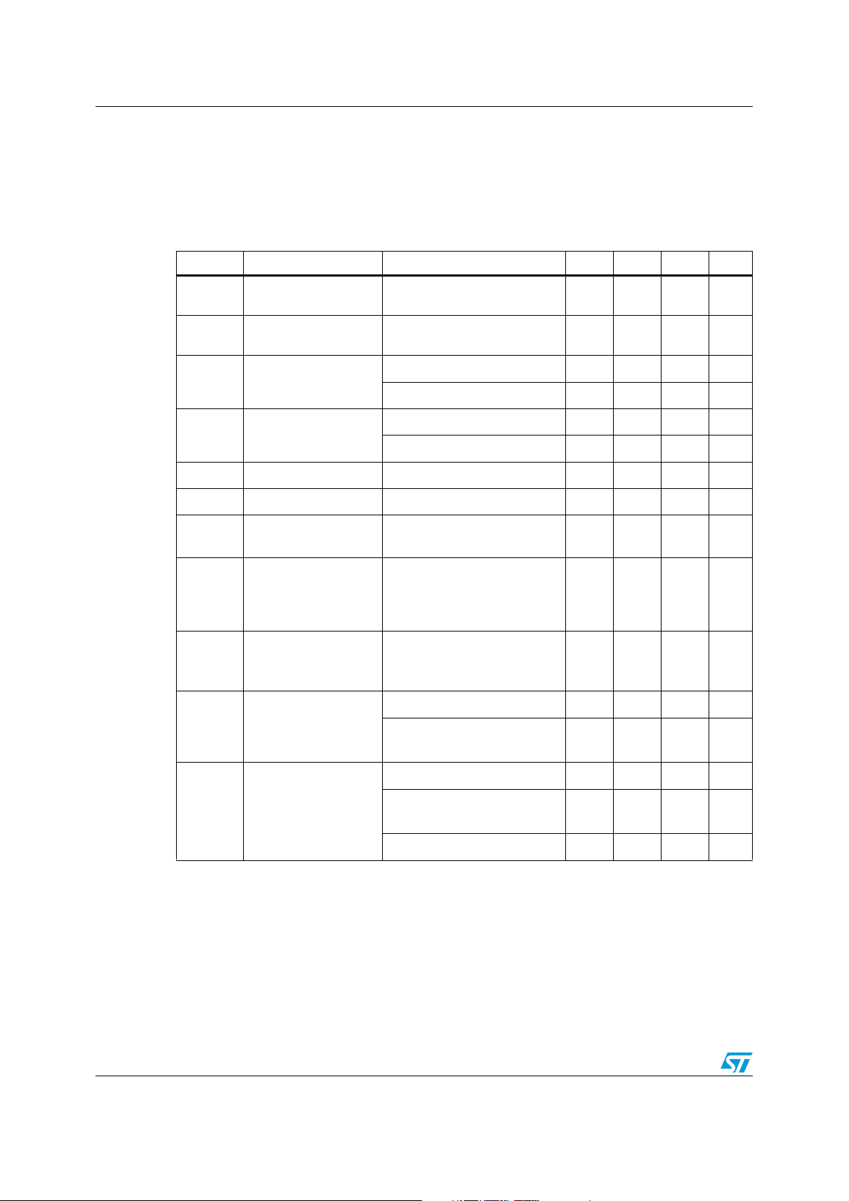
3.1 DC characteristics
Table 5. DC characteristics (V
Symbol Parameter Test conditions Min Typ Max Unit
V
(BR)DSX
V
V
V
I
I
I
CC
I
CC(FRQ)
I
I
DSX
R
DS(on)
Drain-to-source
breakdown voltage
Source-to-drain diode
SD
forward voltage
High level output
OH
voltage SER OUT
Low level output
OL
voltage SER OUT
High level input current
IH
Low level input current
IL
Logic supply current
Logic supply current at
frequency
Nominal current
N
Off-state drain current
Static drain source on
state resistance
(See Note 5, Note 6
and Figure 14,
Figure 16)
= 5 V, TC = 25 °C, unless otherwise specified.)
CC
ID = 1 mA
IF = 100 mA
= -20 μA, VCC = 4.5 V
I
OH
I
= -4 mA, VCC = 4.5 V
OH
IOH = 20 μA, VCC = 4.5 V
I
= 4 mA, VCC = 4.5 V
OH
= 5.5 V, VI = V
V
CC
= 5.5 V, VI = 0
V
CC
CC
VCC = 5.5 V, all outputs OFF or
ON
= 5 MHz, CL = 30 pF
f
SRCK
All outputs OFF
(See Figure 6, Figure 18 and
33 37 V
0.85 1.2 V
4.4 4.49 V
44.2 V
0.005 0.1 V
0.3 0.5 V
20 200 μA
0.2 2 mA
Figure 19)
V
= 0.5 VIN = I
DS(on)
TC = 85 °C
D
90 mA
(See Note 5, Note 6, Note 7)
= 30 V, VCC = 5.5 V
V
DS
V
= 30 V, VCC =5.5 V or 0 V
DS
= 125 °C
T
C
= 50 mA, VCC = 4.5 V
I
D
I
= 50 mA, VCC = 4.5 V
D
= 125 °C
T
C
I
= 100 mA, VCC = 4.5 V
D
0.3 5 μA
0.6 8 μA
4.5 6 Ω
6.5 9 Ω
4.5 6 Ω
1 μA
-1 μA
6/22
Page 7
STPIC6C595 Electrical characteristics
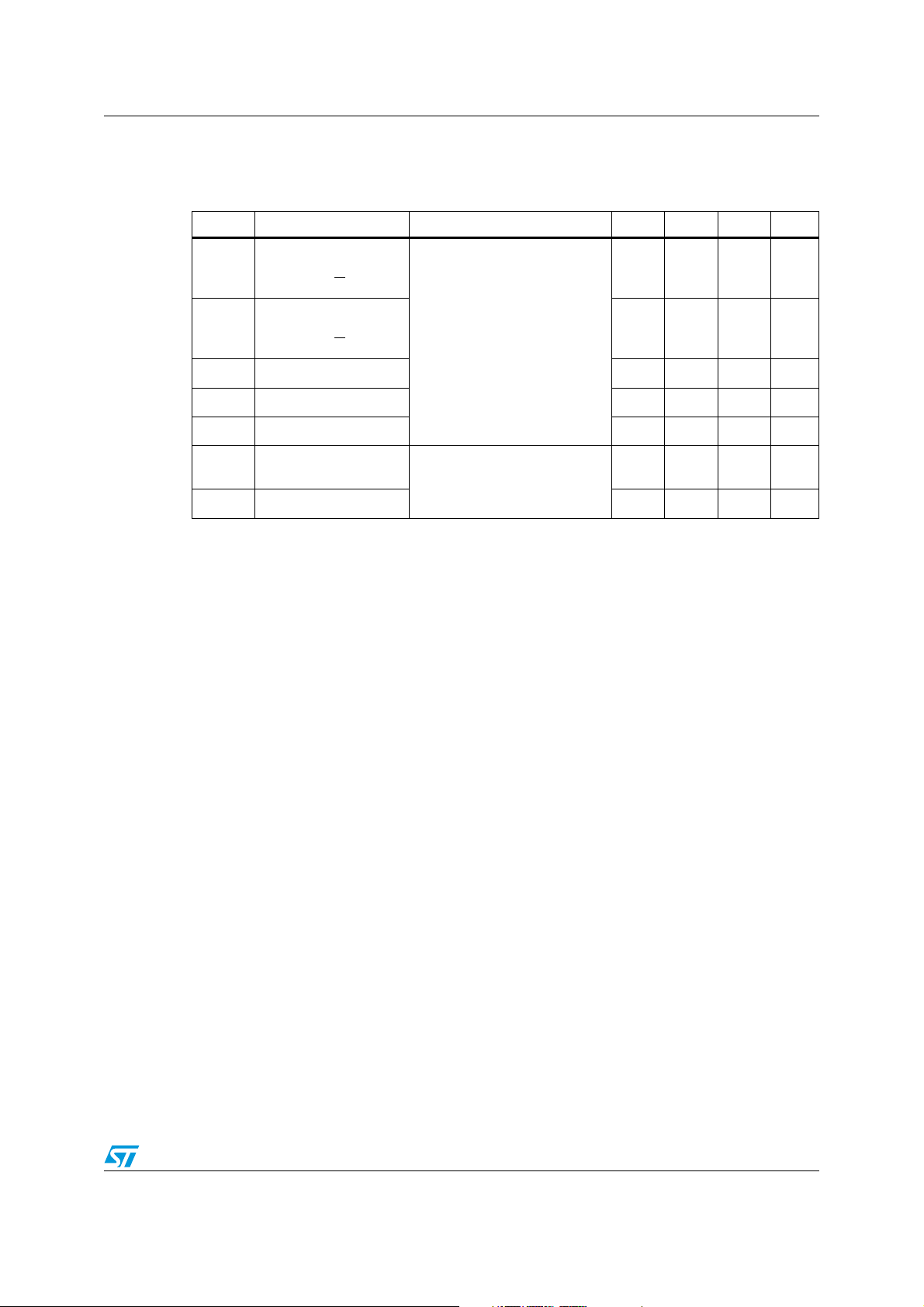
3.2 Switching characteristics
Table 6. Switching characteristics (V
Symbol Parameter Test conditions Min Typ Max Unit
Propagation delay
t
time, high to low level
PHL
output from G
= 5 V, TC = 25 °C, unless otherwise specified.)
CC
80 ns
t
PLH
t
Propagation delay
time, low to high level
output from G
t
Rise time, drain output 60 ns
r
t
Fall time, drain output 50 ns
f
propagation delay time 20 ns
pd
Reverse recovery
t
a
current rise time
t
Reverse recovery time 115 ns
rr
CL = 30 pF, ID = 75 mA
(See Figure 4, Figure 5,
Figure 6, Figure 7, Figure 20)
= 100 mA, di/dt = 10 A/μs
I
F
(See Figure 5, Figure 6, and
Figure 9, Figure 10 )
Note: 1 All voltage value are with respect to GND
2 Each power DMOS source is internally connected to GND
3 Pulse duration
≤
100 μs and duty cycle ≤ 2 %
4 Drain supply voltage = 15 V, starting junction temperature (T
I
= 200 mA (see Fig. 11 and 12)
AS
5 Technique should limit T
- TC to 10 °C maximum
J
6 These parameters are measured with voltage sensing contacts separate from the current-
carrying contacts.
7 Nominal current is defined for a consistent comparison between devices from different
sources. It is the current that produces a voltage drop of 0.5 V at T
130 ns
39 ns
) = 25 °C. L = 1.5 H and
JS
= 85 °C.
C
7/22
Page 8
Logic diagram STPIC6C595
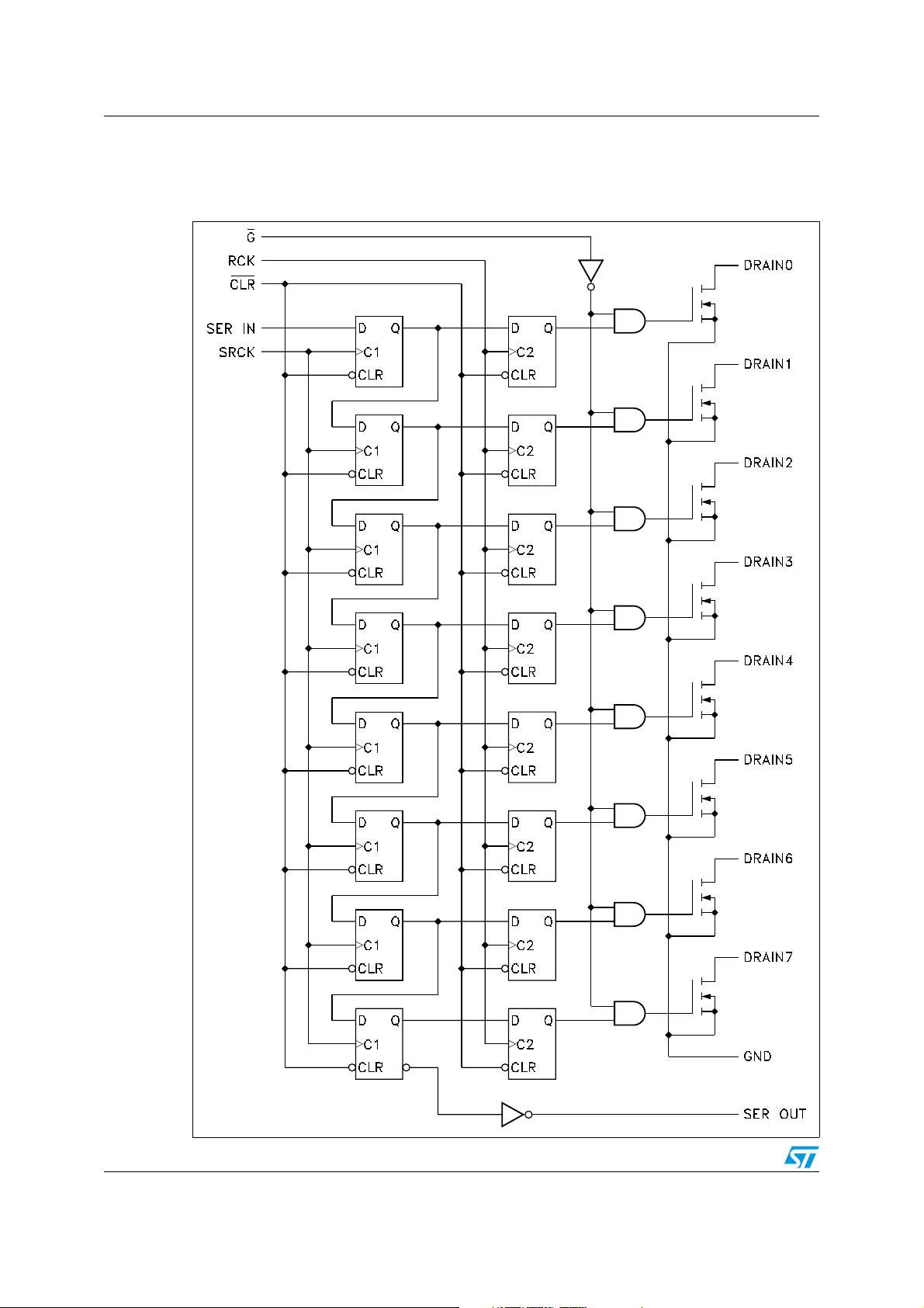
4 Logic diagram
Figure 3. Logic diagram
8/22
Page 9
STPIC6C595 Typical operating circuit
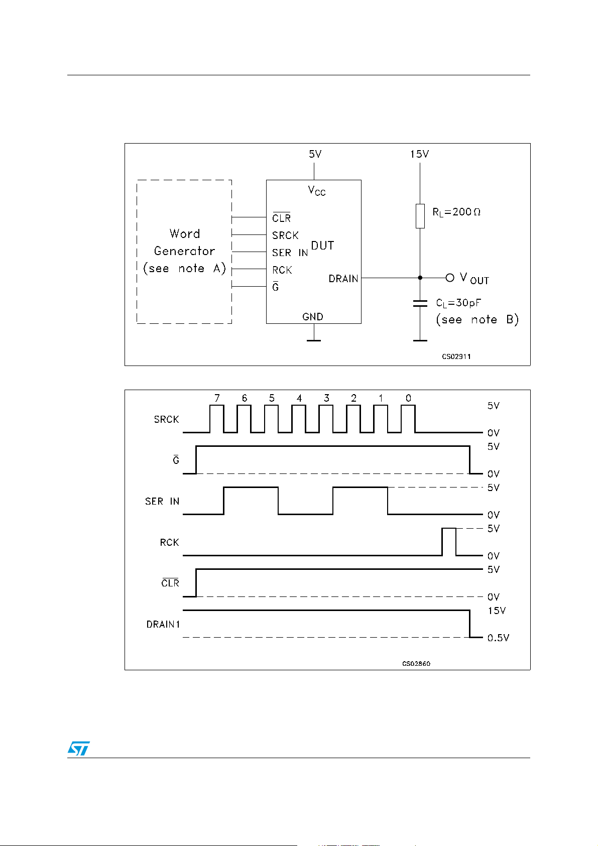
5 Typical operating circuit
Figure 4. Typical operation mode test circuits
Figure 5. Typical operation mode waveforms
Note: 1 A) The word generator has the following characteristics: t
pulse repetition rate (PRR) = 5 kHz, Z
2B) CL includes probe and jig capacitance.
= 50
O
Ω
9/22
≤ 10 ns, tf ≤ 10 ns, tW = 300 ns,
r
Page 10
Typical operating circuit STPIC6C595
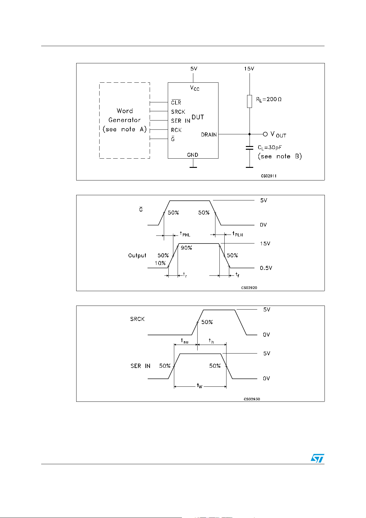
Figure 6. Typical operation mode test circuits
Figure 7. Switching time waveform
Figure 8. Input setup and hold waveform
Note: 1 A) The word generator has the following characteristics: t
pulse repetition rate (PRR) = 5 kHz, Z
= 50
O
Ω
2B) CL includes probe and jig capacitance.
10/22
≤ 10 ns, tf ≤ 10 ns, tW = 300 ns,
r
Page 11
STPIC6C595 Typical operating circuit
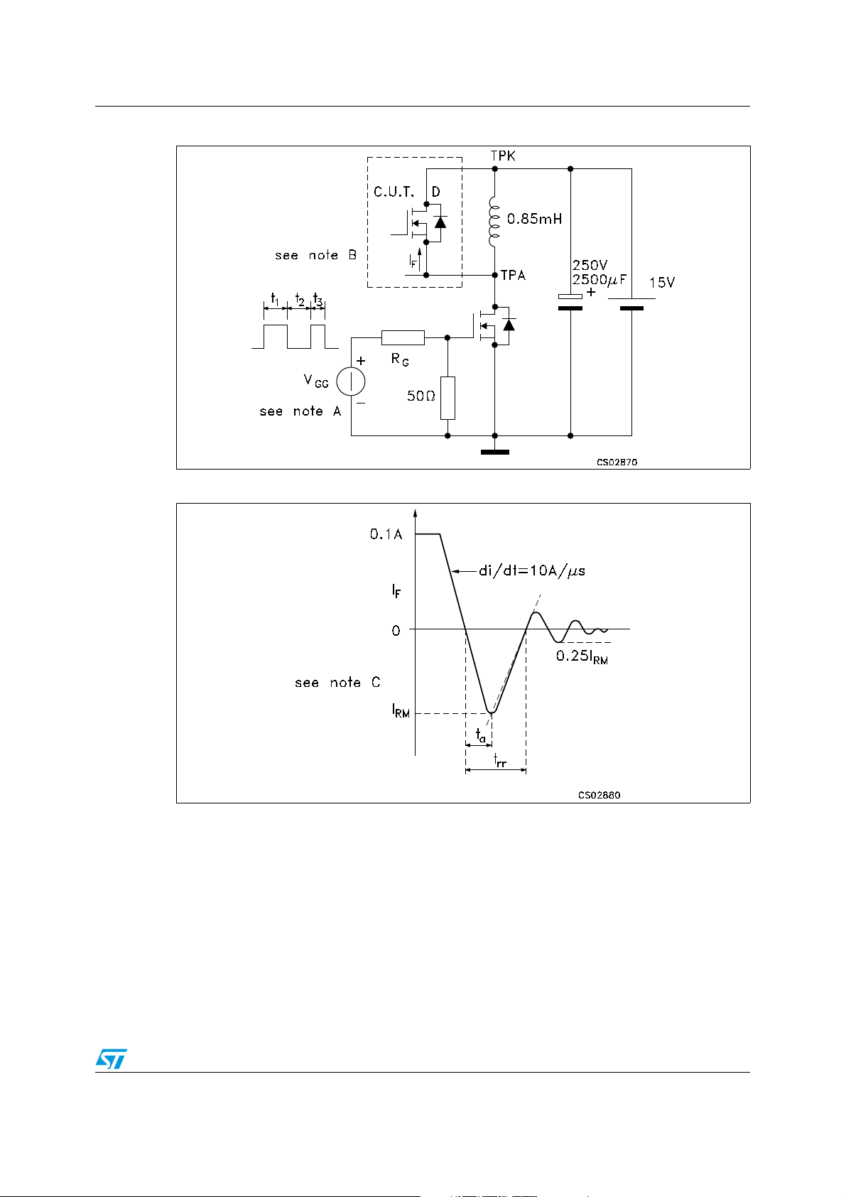
Figure 9. Reverse recovery current test circuits
Figure 10. Source drain diode waveform
Note: 1 A) The V
used to set I
2 B) The drain terminal under test is connected to the TPK test point. All other terminals are
connected together and connected to the TPA test point.
3C) I
= maximum recovery current.
RM
amplitude and RG are adjusted for di/dt = 10 A/μs. A VGG double-pulse train is
GG
= 0.1 A. where t1 = 10 μs, t2 = 7 μs and t3 = 3 μs
F
11/22
Page 12
Typical operating circuit STPIC6C595
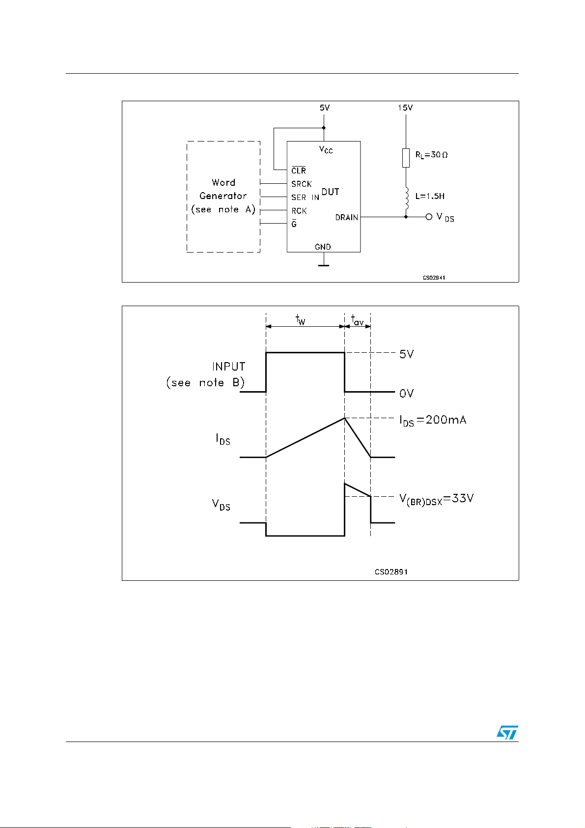
Figure 11. Single pulse avalanche energy test circuits
Figure 12. Single pulse avalanche energy waveform
Note: 1 A) The word generator has the following characteristics: t
2 B) Input pulse duration, tW is increased until peak current IAS = 200 mA. Energy test level is
defined as E
12/22
= (IAS x V
AS
(BR)DSX
x tAV)/2 = 30 mJ.
≤ 10 ns, tf ≤ 10 ns, ZO = 50
r
Ω
Page 13
STPIC6C595 Typical performance and characteristics
6 Typical performance and characteristics
(unless otherwise specified TJ = 25 °C)
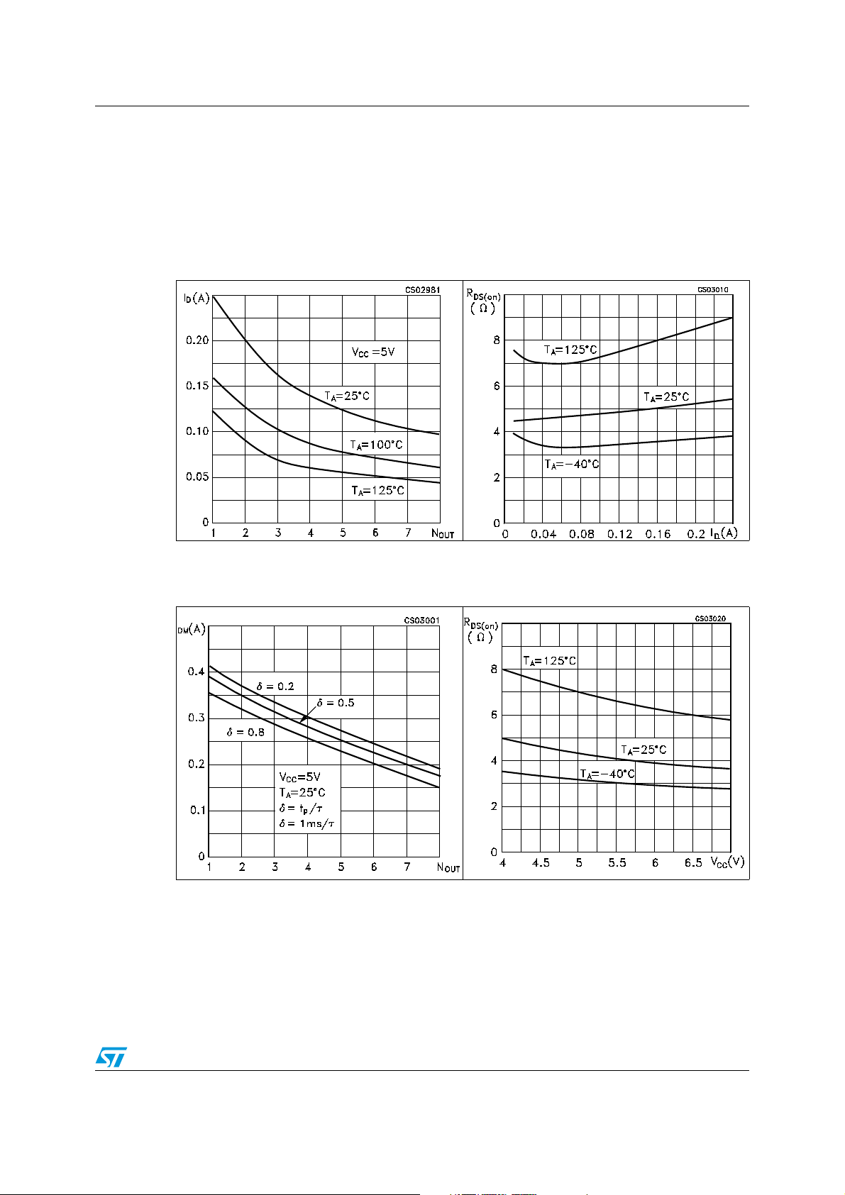
Figure 13. Max continuous drain current
vs number of outputs
conducting simultaneously
Figure 15. Maximum peak drain current
vs number of outputs
conducting simultaneously
Figure 14. Static drain-source on-state
resistance vs drain current
Figure 16. Static drain-source on-state
resistance vs logic supply
voltage
13/22
Page 14
Typical performance and characteristics STPIC6C595
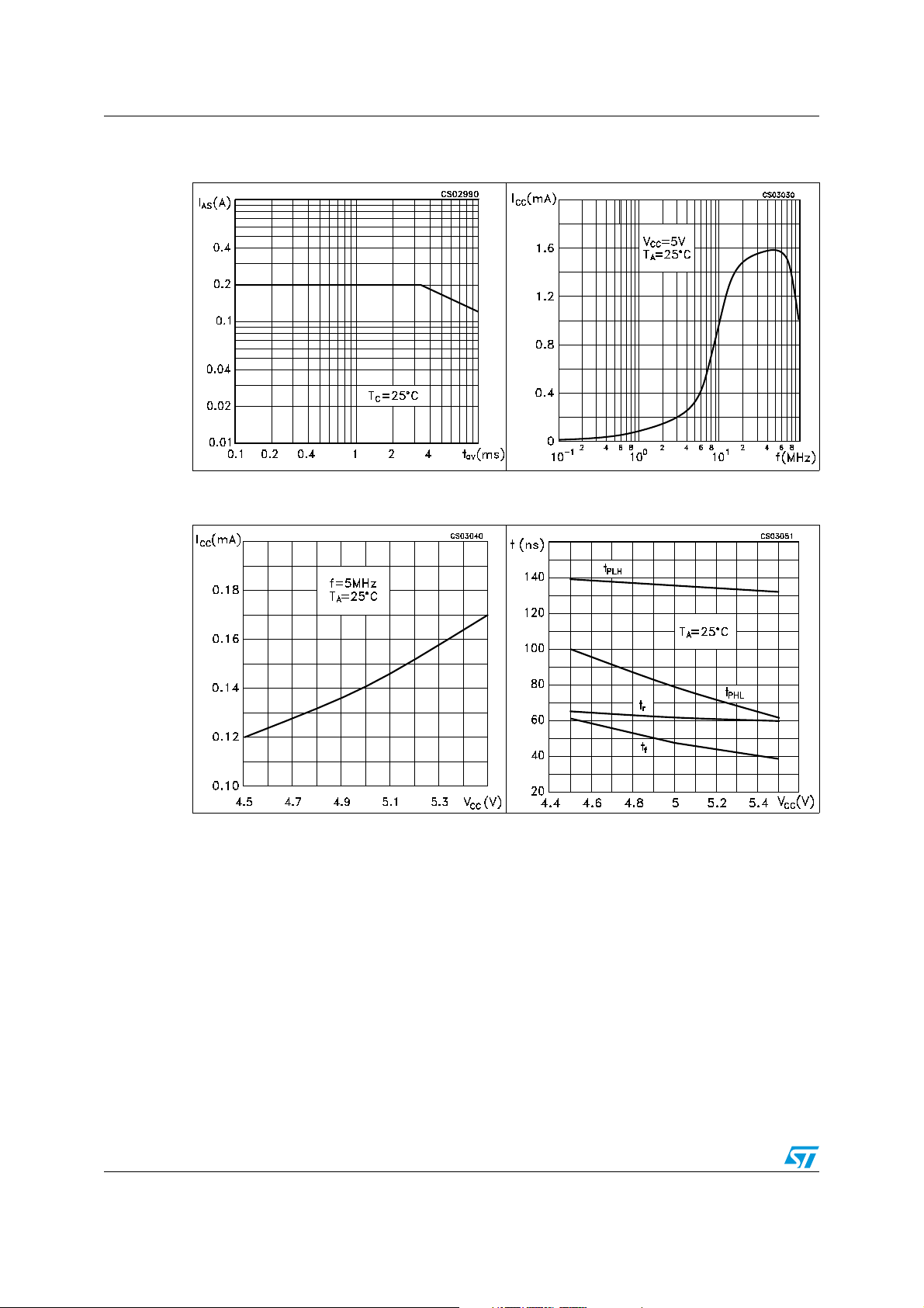
Figure 17. Peak avalanche current vs
time duration of avalanche
Figure 19. Supply current vs
supply voltage
Figure 18. Supply current vs frequency
Figure 20. Switching time vs
case temperature
14/22
Page 15
STPIC6C595 Typical performance and characteristics
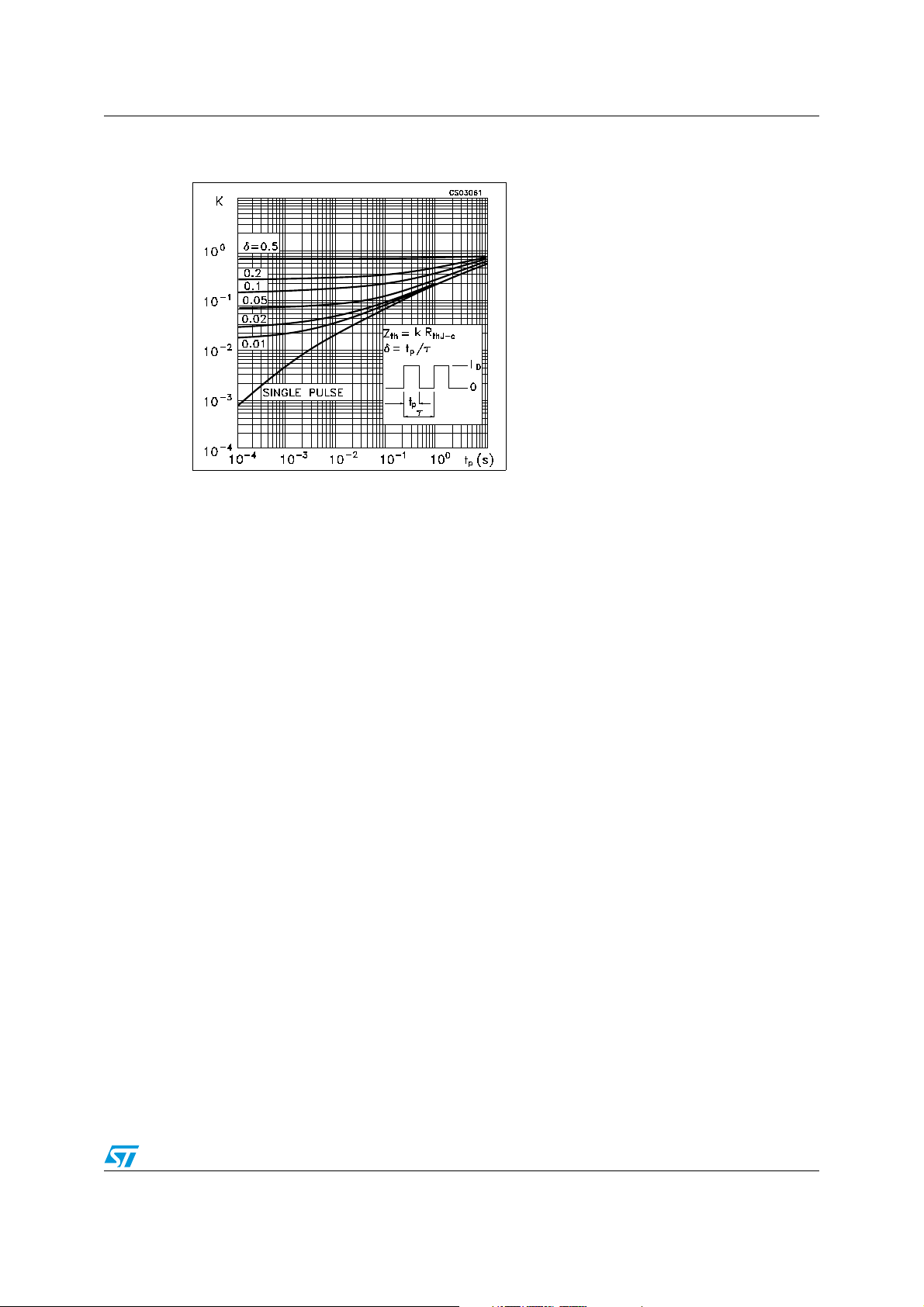
Figure 21. Normalized junction to
ambient thermal resistance
15/22
Page 16

Package mechanical data STPIC6C595
7 Package mechanical data
In order to meet environmental requirements, ST offers these devices in different grades of
ECOPACK® packages, depending on their level of environmental compliance. ECOPACK®
specifications, grade definitions and product status are available at: www.st.com.
ECOPACK® is an ST trademark.
16/22
Page 17
STPIC6C595 Package mechanical data
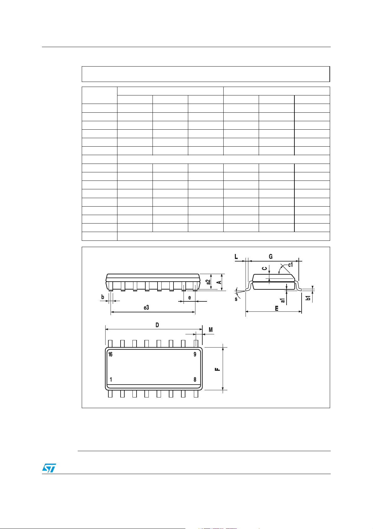
SO-16 MECHANICAL DATA
DIM.
A 1.75 0.068
a1 0.1 0.25 0.004 0.010
a2 1.64 0.063
b 0.35 0.46 0.013 0.018
b1 0.19 0.25 0.007 0.010
C 0.5 0.019
c1 45° (typ.)
D 9.8 10 0.385 0.393
E 5.8 6.2 0.228 0.244
e 1.27 0.050
e3 8.89 0.350
F 3.8 4.0 0.149 0.157
G 4.6 5.3 0.181 0.208
L 0.5 1.27 0.019 0.050
M 0.62 0.024
S8° (max.)
MIN. TYP MAX. MIN. TYP. MAX.
mm. inch
0016020D
17/22
Page 18
Package mechanical data STPIC6C595
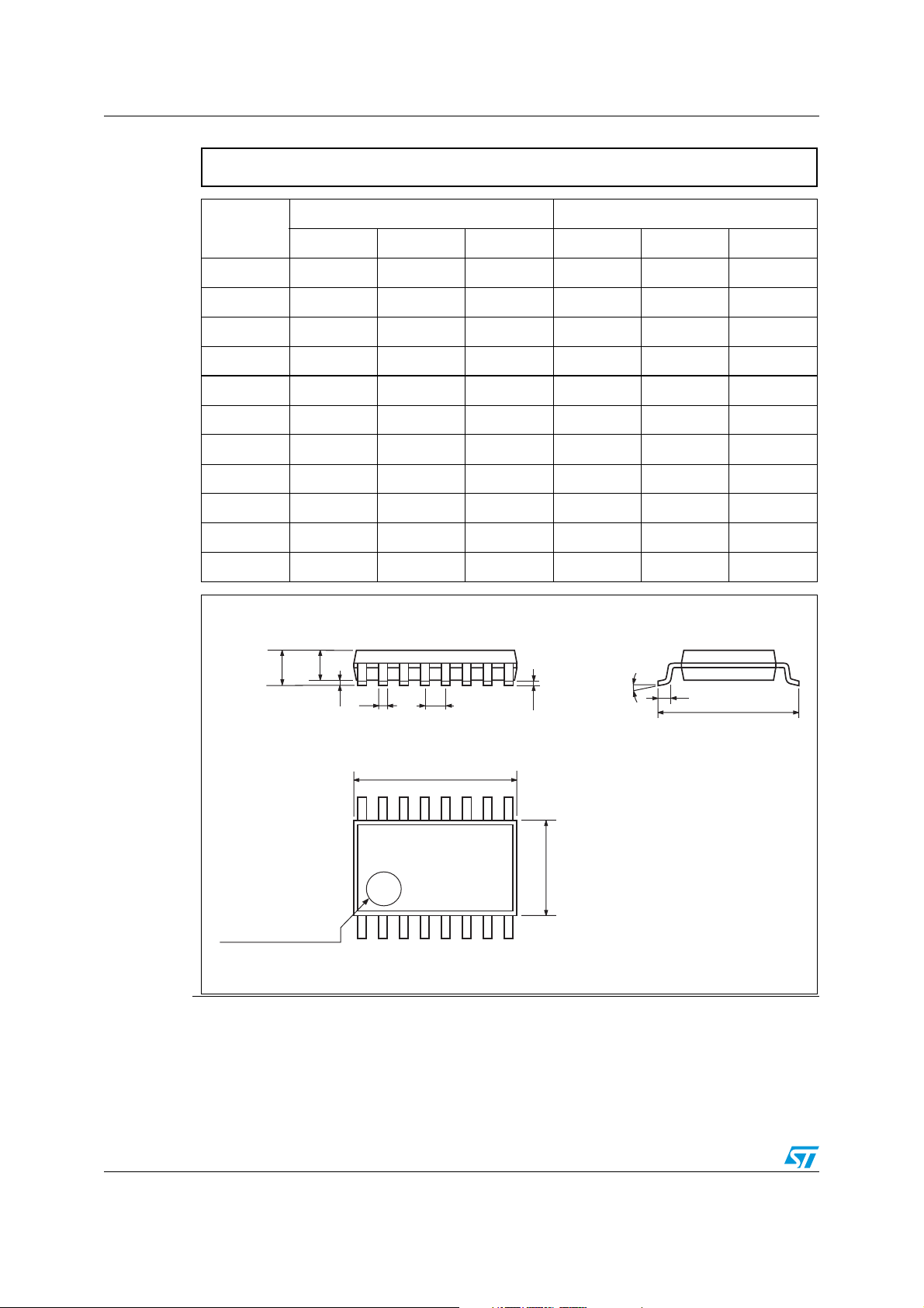
TSSOP16 MECHANICAL DATA
DIM.
MIN. TYP MAX. MIN. TYP. MAX.
A 1.2 0.047
A1 0.05 0.15 0.002 0.004 0.006
A2 0.8 1 1.05 0.031 0.039 0.041
b 0.19 0.30 0.007 0.012
c 0.09 0.20 0.004 0.0079
D 4.9 5 5.1 0.193 0.197 0.201
E 6.2 6.4 6.6 0.244 0.252 0.260
E1 4.3 4.4 4.48 0.169 0.173 0.176
e 0.65 BSC 0.0256 BSC
K0˚ 8˚0˚ 8˚
L 0.45 0.60 0.75 0.018 0.024 0.030
mm. inch
A2
A
PIN 1 IDENTIFICATION
A1
b
e
c
K
L
E
D
E1
1
0080338D
18/22
Page 19
STPIC6C595 Package mechanical data
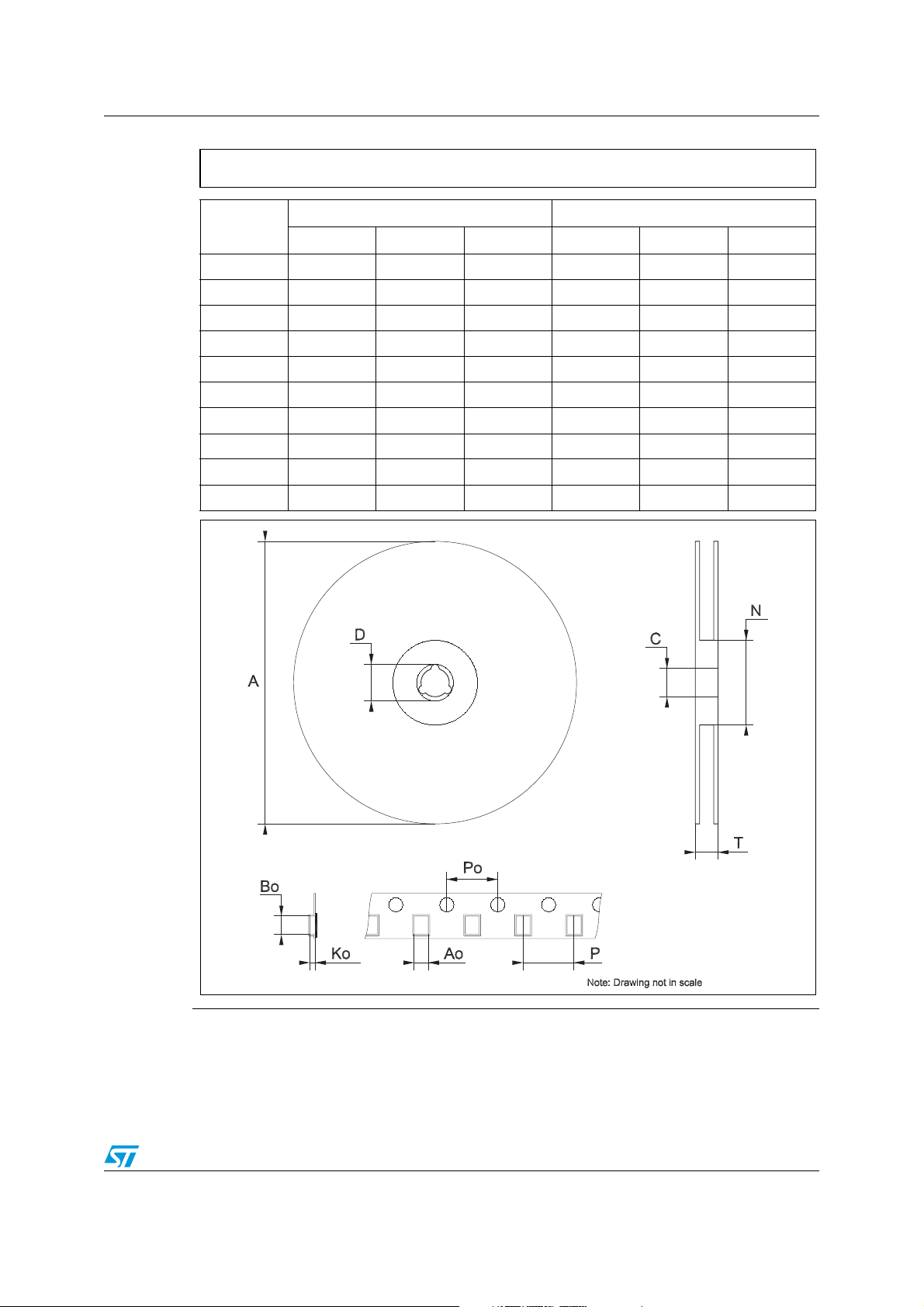
Tape & Reel SO-16 MECHANICAL DATA
DIM.
MIN. TYP MAX. MIN. TYP. MAX.
A 330 12.992
C 12.8 13.2 0.504 0.519
D 20.2 0.795
N 60 2.362
T 22.4 0.882
Ao 6.45 6.65 0.254 0.262
Bo 10.3 10.5 0.406 0.414
Ko 2.1 2.3 0.082 0.090
Po 3.9 4.1 0.153 0.161
P 7.9 8.1 0.311 0.319
mm. inch
19/22
Page 20
Package mechanical data STPIC6C595
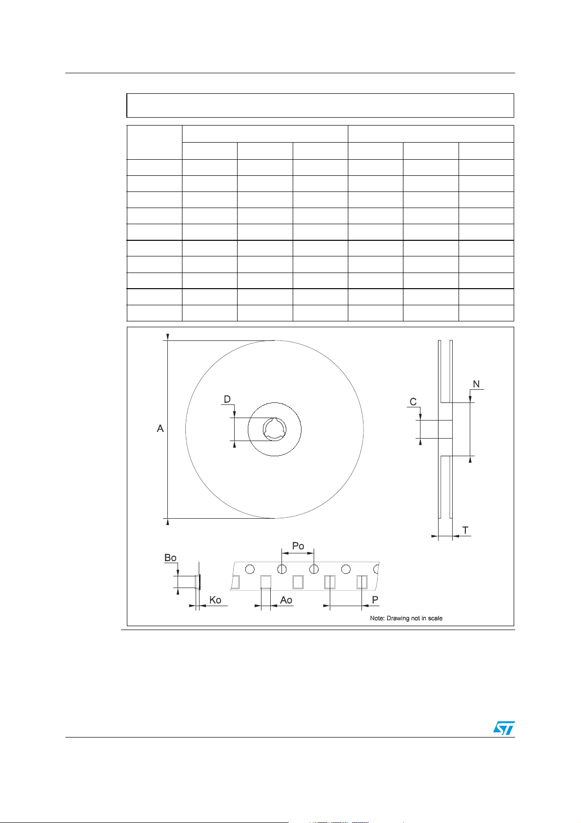
Tape & Reel TSSOP16 MECHANICAL DATA
DIM.
MIN. TYP MAX. MIN. TYP. MAX.
A 330 12.992
C 12.8 13.2 0.504 0.519
D 20.2 0.795
N 60 2.362
T 22.4 0.882
Ao 6.7 6.9 0.264 0.272
Bo 5.3 5.5 0.209 0.217
Ko 1.6 1.8 0.063 0.071
Po 3.9 4.1 0.153 0.161
P 7.9 8.1 0.311 0.319
mm. inch
20/22
Page 21
STPIC6C595 Revision history
8 Revision history
Table 7. Document revision history
Date Revision Changes
07-Jul-2004 2 Update Figure 3
07-May-2007 3 Document reformatted, tube package deleted
21-May-2008 4 Update: tsu and ThL values in Ta bl e 4 , ESD value on cover page
16-Mar-2009 5 Updated Table 5 on page 6
21/22
Page 22

STPIC6C595
Please Read Carefully:
Information in this document is provided solely in connection with ST products. STMicroelectronics NV and its subsidiaries (“ST”) reserve the
right to make changes, corrections, modifications or improvements, to this document, and the products and services described herein at any
time, without notice.
All ST products are sold pursuant to ST’s terms and conditions of sale.
Purchasers are solely responsible for the choice, selection and use of the ST products and services described herein, and ST assumes no
liability whatsoever relating to the choice, selection or use of the ST products and services described herein.
No license, express or implied, by estoppel or otherwise, to any intellectual property rights is granted under this document. If any part of this
document refers to any third party products or services it shall not be deemed a license grant by ST for the use of such third party products
or services, or any intellectual property contained therein or considered as a warranty covering the use in any manner whatsoever of such
third party products or services or any intellectual property contained therein.
UNLESS OTHERWISE SET FORTH IN ST’S TERMS AND CONDITIONS OF SALE ST DISCLAIMS ANY EXPRESS OR IMPLIED
WARRANTY WITH RESPECT TO THE USE AND/OR SALE OF ST PRODUCTS INCLUDING WITHOUT LIMITATION IMPLIED
WARRANTIES OF MERCHANTABILITY, FITNESS FOR A PARTICULAR PURPOSE (AND THEIR EQUIVALENTS UNDER THE LAWS
OF ANY JURISDICTION), OR INFRINGEMENT OF ANY PATENT, COPYRIGHT OR OTHER INTELLECTUAL PROPERTY RIGHT.
UNLESS EXPRESSLY APPROVED IN WRITING BY AN AUTHORIZED ST REPRESENTATIVE, ST PRODUCTS ARE NOT
RECOMMENDED, AUTHORIZED OR WARRANTED FOR USE IN MILITARY, AIR CRAFT, SPACE, LIFE SAVING, OR LIFE SUSTAINING
APPLICATIONS, NOR IN PRODUCTS OR SYSTEMS WHERE FAILURE OR MALFUNCTION MAY RESULT IN PERSONAL INJURY,
DEATH, OR SEVERE PROPERTY OR ENVIRONMENTAL DAMAGE. ST PRODUCTS WHICH ARE NOT SPECIFIED AS "AUTOMOTIVE
GRADE" MAY ONLY BE USED IN AUTOMOTIVE APPLICATIONS AT USER’S OWN RISK.
Resale of ST products with provisions different from the statements and/or technical features set forth in this document shall immediately void
any warranty granted by ST for the ST product or service described herein and shall not create or extend in any manner whatsoever, any
liability of ST.
ST and the ST logo are trademarks or registered trademarks of ST in various countries.
Information in this document supersedes and replaces all information previously supplied.
The ST logo is a registered trademark of STMicroelectronics. All other names are the property of their respective owners.
© 2009 STMicroelectronics - All rights reserved
STMicroelectronics group of companies
Australia - Belgium - Brazil - Canada - China - Czech Republic - Finland - France - Germany - Hong Kong - India - Israel - Italy - Japan -
Malaysia - Malta - Morocco - Singapore - Spain - Sweden - Switzerland - United Kingdom - United States of America
www.st.com
22/22
 Loading...