

Page 1
STP80NS04Z
N - CHANNEL CLAMPED 7.5mΩ - 80A - TO-220
FULLY PROTECTED MESH OVERLAY MOSFET
TYPE V
DSS
R
DS(on)
I
D
ST P80NS04Z CLAMP ED <0.0 08 Ω 80 A
■ TYPICALR
■ 100%AVALANCHETESTED
■ LOW CAPACITANCEAND GATECHARGE
■ 175
o
C MAXIMUMJUNCTION
DS(on)
= 0.0075 Ω
TEMPERATURE
DESCRIPTION
This fully clamped Mosfet is produced by using
the latest advanced Company’s Mesh Overlay
processwhich is based on a novelstrip layout.
The inherent benefits of the new technology
coupledwith the extra clamping capabilitiesmake
this product particularly suitable for the harshest
operation conditions such as those encountered
in the automotive environment. Any other
application requiring extra ruggedness is also
recommended.
APPLICATIONS
■ ABS, SOLENOIDDRIVERS
■ MOTORCONTROL
■ DC-DCCONVERTERS
3
2
1
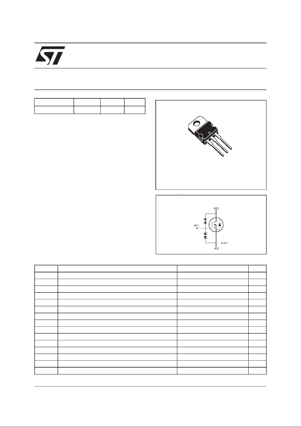
TO-220
INTERNAL SCHEMATIC DIAGRAM
ABSOLUTE MAXIMUM RATINGS
Symbol Parameter Value Unit
V
V
V
I
I
I
DM
P
V
ESD
V
ESD
V
ESD
T
(•) Pulse width limited by safeoperating area (1)ISD≤ 80 A, di/dt ≤ 300 A/µs, VDD≤ V
December 1999
Dra in- sour c e Voltage (VGS= 0) CLAMPED V
DS
Drain- gate Voltage CLAMPED V
DG
Gate-s ource Volt age CLAMPED V
GS
Dra in Current (conti nuous) at Tc=25oC80A
I
D
Dra in Current (conti nuous) at Tc= 100oC60A
I
D
Dra in Gate Cur rent ( continuous )
DG
Gat e Source Current (continuous ) ± 50 mA
GS
50 mA
±
(•) Dra in Current (pulsed) 320 A
Tot al Dissipatio n at Tc=25oC 160 W
tot
Der ati ng Fac t or 1.06 W/
Gat e- Source ESD (H B M - C= 100pF , R=1.5 kΩ)2kV
(G-S)
(G-D) G at e-Drain ESD (H BM - C= 100pF , R=1.5 kΩ)4kV
(D-S) Drain-Sour ce ESD (HB M - C= 100p F, R=1.5 kΩ)4kV
St orage Temperat ur e -65 to 175
stg
Max. Operat ing Junc tion Tempe ra t ure -40 to 175
T
j
(BR)DSS,Tj≤TJMAX
o
C
o
C
o
C
1/8
Page 2

STP80NS04Z
THERMAL DATA
R
thj-case
R
thj-case
R
thj-amb
R
thc-sink
T
AVALANCHE CHARACTERISTICS
Symbol Parameter Max Value Unit
I
AR
E
Ther mal Resistance J unction- ca se Max
Ther mal Resistance J unction- ca se Ty p
Ther mal Resistance J unction- am bie nt M a x
Ther mal Resistance C ase-sink Ty p
Maximum Lead Te mperature For Solder ing Purp os e
l
Avalanche Current, R epetitive or Not-Repetitive
(pulse width limited by T
Single P ul s e Avalanche Energy
AS
(starting T
=25oC, ID=IAR,VDD=30V)
j
max, δ <1%)
j
0.94
0.65
62.5
0.5
300
80 A
500 mJ
o
C/W
o
C/W
o
C/W
o
C/W
o
C
ELECTRICAL CHARACTERISTICS
=25oC unless otherwisespecified)
(T
case
OFF
Symbol Parameter Test Conditions Min. Typ. Max. Unit
V
CLAMP
I
DSS
I
GSS
V
GSS
Drain-G ate Breakdown
Voltage
Zero Gate Voltage
Drain Cur rent ( V
GS
=0)
Gat e- bod y L eak ag e
Current (V
DS
=0)
Gate-Source
ID=1mA VGS=0
-40 < T
V
V
V
< 175oC
j
=16V Tj= 175oC50µA
DS
=± 10 V Tj=175oC
GS
= ± 16 V Tj=175oC
GS
33 V
50
150
IG= 100 µA18V
Break dow n Volt age
ON(∗)
Symbol Parameter Test Conditions Min. Typ. Max. Unit
V
GS(th)
R
DS(on)
I
D(on)
Gate Threshold Voltage VDS=V
-40 < T
Sta t ic Drain -s ource On
Resistance
VGS=10V ID=40A
=16V ID=40A
V
GS
On State Drain Current VDS>I
GSID
=1mA
< 150oC
j
D(on)xRDS(on)max
1.7 3 4.2 V
8
7.5
9
8
80 A
VGS=10V
DYNAMIC
µ
µA
mΩ
m
A
Ω
Symbol Parameter Test Conditions Min. Typ. Max. Unit
g
(∗)Forward
fs
VDS>I
D(on)xRDS(on)maxID
=40 A 30 50 S
Tr ansc on duc tance
C
C
C
Input Capac i t ance
iss
Out put Capacitanc e
oss
Reverse Tr ansfer
rss
VDS=25V f=1MHz VGS= 0 4000
1250
230
5400
1700
320
Capacit a nc e
2/8
pF
pF
pF
Page 3

STP80NS04Z
ELECTRICAL CHARACTERISTICS
(continued)
SWITCHING ON
Symbol Parameter Test Conditions Min. Typ. Max. Unit
Q
Q
Q
Tot al Gat e Charge
g
Gat e- Source Charg e
gs
Gate-Drain Charge
gd
VDD=16V ID=80A VGS= 10 V 105
24
41
142 nC
SWITCHING OFF
Symbol Parameter Test Conditions Min. Typ. Max. Unit
t
r(Voff)
t
Off-voltage Rise Time
Fall T ime
t
f
Cross-over T ime
c
V
R
=30V ID=80A
CLAM P
=4.7 ΩVGS=10V
G
(see test circuit, figure 5)
60
140
220
80
190
300
SOURCEDRAINDIODE
Symbol Parameter Test Conditions Min. Typ. Max. Unit
I
SD
I
SDM
V
SD
t
Q
I
RRM
(∗) Pulsed:Pulse duration = 300µs, duty cycle 1.5%
(•) Pulse width limited by safe operating area
Source-drain Current
(•)
Source-drain Current
80
320
(pulsed)
(∗)ForwardOnVoltage ISD=80A VGS=0 1.5 V
Reverse Recovery
rr
Time
Reverse Recovery
rr
ISD= 80 A di/dt = 100 A/µs
=25V Tj= 150oC
V
r
(see test circuit, figure 5)
75
0.21
Charge
Reverse Recovery
6
Current
nC
nC
ns
ns
ns
A
A
ns
µ
A
C
SafeOperating Area ThermalImpedance
3/8
Page 4

STP80NS04Z
OutputCharacteristics
Transconductance
TransferCharacteristics
Static Drain-sourceOn Resistance
Gate Charge vs Gate-sourceVoltage
4/8
CapacitanceVariations
Page 5

STP80NS04Z
NormalizedGate ThresholdVoltage vs
Temperature
ZeroGate VoltageDrain Current vs
Temperature
NormalizedOn Resistancevs Temperature
Source-drainDiode ForwardCharacteristics
5/8
Page 6

STP80NS04Z
Fig. 1:
UnclampedInductiveLoad TestCircuit
Fig. 3: SwitchingTimes Test Circuits For
ResistiveLoad
Fig. 2:
UnclampedInductive Waveform
Fig. 4: Gate Chargetest Circuit
Fig. 5:
Test Circuit For InductiveLoad Switching
And Diode Recovery Times
6/8
Page 7

TO-220 MECHANICAL DATA
STP80NS04Z
DIM.
MIN. TYP. MAX. MIN. TYP. MAX.
A 4.40 4.60 0.173 0.181
C 1.23 1.32 0.048 0.051
D 2.40 2.72 0.094 0.107
D1 1.27 0.050
E 0.49 0.70 0.019 0.027
F 0.61 0.88 0.024 0.034
F1 1.14 1.70 0.044 0.067
F2 1.14 1.70 0.044 0.067
G 4.95 5.15 0.194 0.203
G1 2.4 2.7 0.094 0.106
H2 10.0 10.40 0.393 0.409
L2 16.4 0.645
L4 13.0 14.0 0.511 0.551
L5 2.65 2.95 0.104 0.116
L6 15.25 15.75 0.600 0.620
L7 6.2 6.6 0.244 0.260
L9 3.5 3.93 0.137 0.154
DIA. 3.75 3.85 0.147 0.151
mm inch
E
A
L4
D
F2
F1
G1
H2
G
F
P011C
C
D1
L2
Dia.
L5
L7
L6
L9
7/8
Page 8

STP80NS04Z
Information furnishedis believed to be accurateand reliable.However, STMicroelectronics assumes no responsibilityforthe consequences
of use of such information nor for any infringement of patents or other rights of third parties which may result from its use. No license is
granted by implication orotherwise under any patent or patent rights of STMicroelectronics. Specificationmentioned in this publication are
subjectto change without notice.Thispublication supersedes and replacesall information previouslysupplied. STMicroelectronics products
are not authorized for use as critical components in life support devicesor systemswithout express written approval of STMicroelectronics.
The STlogo is a trademark of STMicroelectronics
1999 STMicroelectronics – Printed in Italy – All Rights Reserved
STMicroelectronics GROUP OF COMPANIES
Australia - Brazil - China - Finland - France - Germany - Hong Kong - India - Italy - Japan - Malaysia - Malta - Morocco -
8/8
Singapore - Spain - Sweden- Switzerland - United Kingdom - U.S.A.
http://www.st.com
.
 Loading...