

Page 1
STP80NF55L-06
N - CHANNEL 55V - 0.005 Ω - 80A TO-220
STripFET POWER MOSFET
TYPE V
DSS
R
DS(on)
I
D
ST P80NF55L-06 55 V < 0.006 5 Ω 80 A
■ TYPICALR
■ LOW THRESHOLDDRIVE
■ LOGICLEVEL DEVICE
DS(on)
= 0.005 Ω
DESCRIPTION
This PowerMOSFET is the latest developmentof
STMicroelectronics unique ”Single Feature
Size” strip-based process. The resulting
transistor shows extremely high packing density
for low on-resistance, rugged avalanche
characteristics and less critical alignment steps
therefore a remarkable manufacturing
reproducibility.
APPLICATIONS
■ HIGHCURRENT, HIGH SPEED SWITCHING
■ SOLENOIDAND RELAYDRIVERS
■ MOTORCONTROL, AUDIO AMPLIFIERS
■ DC-DC& DC-ACCONVERTERS
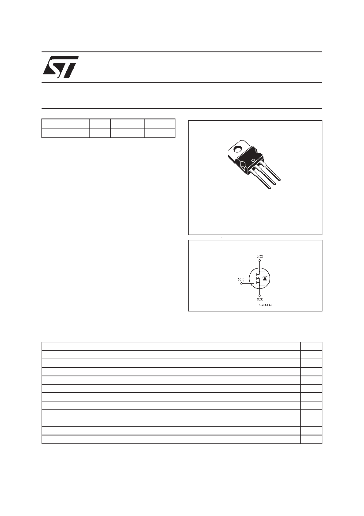
3
2
1
TO-220
INTERNAL SCHEMATIC DIAGRAM
ABSOLUTE MAXIMUM RATINGS
Symbol Parameter Value Uni t
V
V
V
I
DM
P
E
AS
T
(•) Pulse width limitedby safe operating area (1) starting Tj
October 1999
Dra in- sour c e Volta ge (VGS=0) 55 V
DS
Drain- gate Voltage (RGS=20kΩ)55V
DGR
Gate-s ource Volt age ± 20 V
GS
Dra in Cu rr ent (continuous) at Tc=25oC80A
I
D
Dra in Cu rr ent (continuous) at Tc= 100oC57A
I
D
(
Dra in Cu rr ent (pulsed) 320 A
•)
Tot al Dissi pat io n at Tc=25oC 210 W
tot
Der ati ng Fa c t or 1.4 W/
(1) Single Pu lse Avalanche E n ergy 1 J
St orage Tem pe ra t ure -65 to 175
stg
Max. Operating Junction Tem pe ra t ure 175
T
j
=25oC,ID=40A , VDD= 30V
o
C
o
C
o
C
1/8
Page 2
STP80NF55L-06
THERMAL DATA
R
thj-case
R
thj-amb
T
Ther mal Resistanc e Junct ion-case Max
Ther mal Resistanc e Junct ion-ambient Max
Maximum L ead Temperature For So ldering Purpos e
l
0.71
62.5
300
o
C/W
o
C/W
o
C
ELECTRICAL CHARACTERISTICS
=25oC unless otherwisespecified)
(T
case
OFF
Symbol Parameter Test Conditions Min. Typ. Max. U nit
V
(BR)DSS
Drain-source
ID=250µAVGS=0 55 V
Break dow n Vo lt age
I
DSS
I
GSS
Zero Gate Voltage
Drain Curre nt (V
GS
Gat e- bod y Leakag e
Current (V
DS
=0)
=0)
V
=MaxRating
DS
=MaxRating Tc=125oC
V
DS
V
= ± 20 V ± 100 nA
GS
1
10
ON(∗)
Symbol Parameter Test Conditions Min. Typ. Max. U nit
V
GS(th)
R
DS(on)
I
D(on)
Gate Threshold Voltage VDS=VGSID= 250 µ A11.62.5V
Sta t ic Drain-s our c e On
Resistance
On State Drain Current VDS>I
VGS=10V ID=40A
V
=5V ID=40A
GS
D(on)xRDS(on )max
0.005
0.0055
0.0065
0.008
80 A
VGS=10V
DYNAMIC
Symbol Parameter Test Conditions Min. Typ. Max. U nit
g
(∗)Forward
fs
Tr ansc on duc tance
C
C
C
Input Capaci t ance
iss
Out put Capac itance
oss
Reverse Transfer
rss
Capacit a nc e
VDS>I
D(on)xRDS(on )maxID
=18 A 20 S
VDS=25V f=1MHz VGS= 0 7600
990
270
µA
µ
Ω
Ω
pF
pF
pF
A
2/8
Page 3
STP80NF55L-06
ELECTRICAL CHARACTERISTICS
(continued)
SWITCHINGON
Symbol Parameter Test Conditions Min. Typ. Max. U nit
t
d(on)
Tur n-on Delay Time
Rise Time
t
r
VDD=27V ID=40A
R
=4.7
G
Ω
VGS=4.5V
75
300
(Resis t iv e Load, see fig. 3)
Q
Q
Q
Tot al Gate Charge
g
Gat e- Source Char g e
gs
Gate-Drain Charge
gd
VDD=44V ID=80A VGS=5V 97
25
46
100 nC
SWITCHINGOFF
Symbol Parameter Test Conditions Min. Typ. Max. U nit
t
d(off)
Tur n-of f Dela y Tim e
t
Fall T ime
f
VDD=27V ID=40A
=4.7 Ω VGS=4.5V
R
G
210
160
(Resis t iv e Load, see fig. 3)
t
d(off)
Off-volt age Rise Time
t
Fall T ime
f
t
Cross-over Tim e
c
Vclamp = 44 V ID=80A
=4.7 Ω VGS=4.5V
R
G
(Indu ct iv e Load, see fig . 5)
90
230
350
SOURCEDRAIN DIODE
Symbol Parameter Test Conditions Min. Typ. Max. U nit
I
V
I
SDM
SD
Q
I
RRM
SD
t
Source-drain Current
(•)
Source-drain Current
80
320
(pulsed)
(∗)ForwardOnVoltage ISD=80A VGS=0 1.5 V
Reverse Recovery
rr
Time
Reverse Recovery
rr
ISD= 80 A di/dt = 100 A /µs
=25V Tj=150oC
V
DD
(see test circuit, fig. 5)
75
190
Charge
Reverse Recovery
5.1
Current
ns
ns
nC
nC
ns
ns
ns
ns
ns
A
A
ns
nC
A
(∗) Pulsed: Pulse duration = 300 µs, duty cycle 1.5%
(•) Pulse width limited by safeoperating area
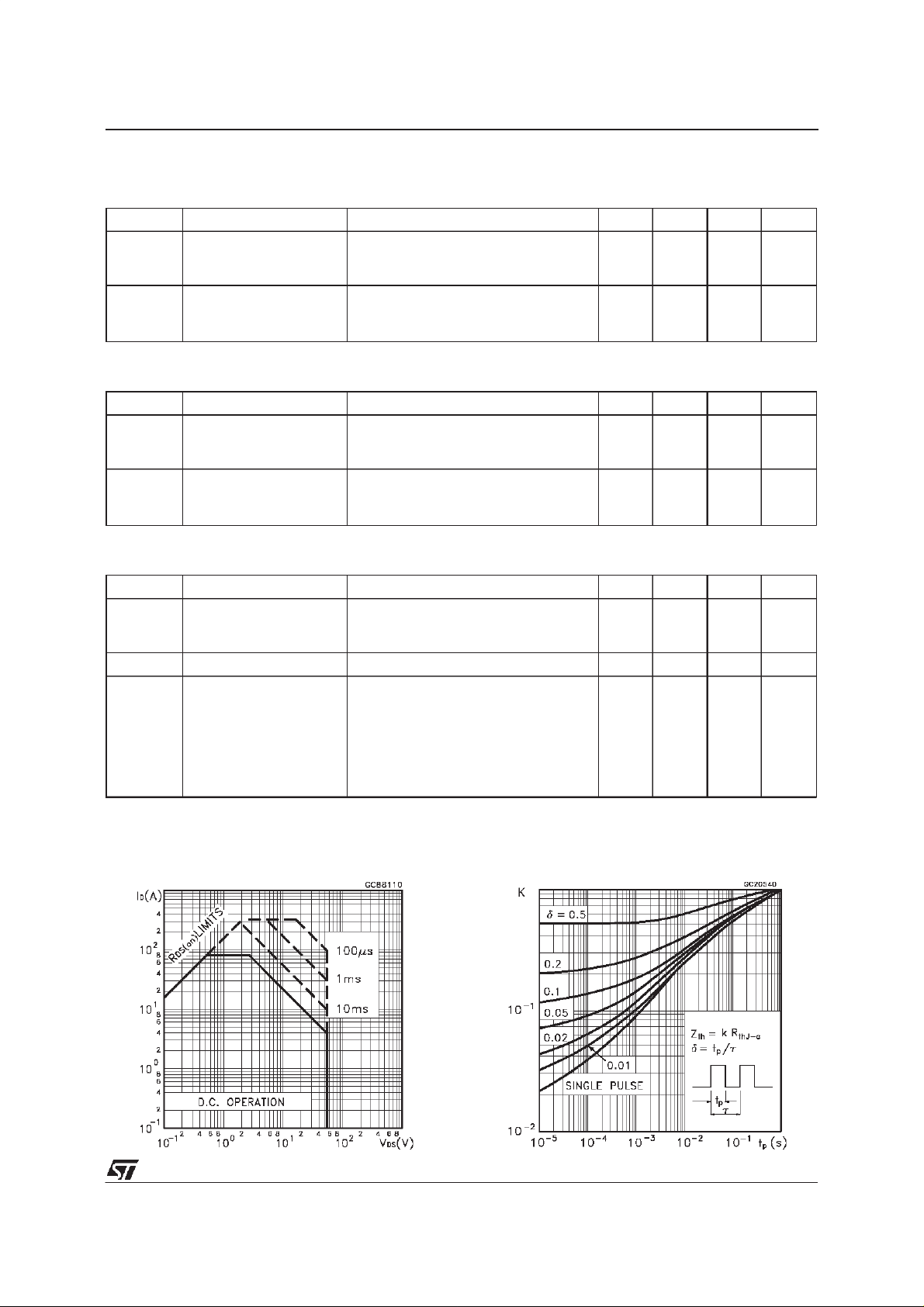
SafeOperating Area ThermalImpedance
3/8
Page 4

STP80NF55L-06
OutputCharacteristics
Transconductance
TransferCharacteristics
Static Drain-sourceOn Resistance
Gate Charge vs Gate-sourceVoltage
4/8
CapacitanceVariations
Page 5

STP80NF55L-06
NormalizedGate ThresholdVoltage vs
Temperature
Source-drainDiode Forward Characteristics
NormalizedOn Resistancevs Temperature
5/8
Page 6

STP80NF55L-06
Fig. 1: UnclampedInductiveLoad Test Circuit
Fig. 3: SwitchingTimesTest CircuitsFor
ResistiveLoad
Fig. 2:UnclampedInductive Waveform
Fig. 4: Gate Charge test Circuit
Fig. 5: TestCircuit ForInductiveLoad Switching
And Diode Recovery Times
6/8
Page 7

TO-220 MECHANICALDATA
STP80NF55L-06
DIM.
MIN. TYP. MAX. MIN. TYP. MAX.
A 4.40 4.60 0.173 0.181
C 1.23 1.32 0.048 0.051
D 2.40 2.72 0.094 0.107
D1 1.27 0.050
E 0.49 0.70 0.019 0.027
F 0.61 0.88 0.024 0.034
F1 1.14 1.70 0.044 0.067
F2 1.14 1.70 0.044 0.067
G 4.95 5.15 0.194 0.203
G1 2.4 2.7 0.094 0.106
H2 10.0 10.40 0.393 0.409
L2 16.4 0.645
L4 13.0 14.0 0.511 0.551
L5 2.65 2.95 0.104 0.116
L6 15.25 15.75 0.600 0.620
L7 6.2 6.6 0.244 0.260
L9 3.5 3.93 0.137 0.154
DIA. 3.75 3.85 0.147 0.151
mm inch
E
A
L4
D
F2
F1
G1
H2
G
F
P011C
C
D1
L2
Dia.
L5
L7
L6
L9
7/8
Page 8

STP80NF55L-06
Information furnished is believed tobeaccurateand reliable. However, STMicroelectronics assumesno responsibility for the consequences
of use of such information nor for any infringement of patents or other rights of third parties which may resultfrom its use. No license is
granted by implication or otherwise under any patent or patent rights of STMicroelectronics. Specificationmentioned in this publicationare
subjecttochange without notice.Thispublication supersedesand replacesall information previouslysupplied.STMicroelectronics products
are not authorizedfor useas critical components in lifesupport devices or systems without express written approval of STMicroelectronics.
The STlogo is a trademark of STMicroelectronics
1999STMicroelectronics – Printed in Italy – All Rights Reserved
STMicroelectronics GROUP OF COMPANIES
Australia - Brazil - China- Finland - France - Germany - Hong Kong - India - Italy - Japan - Malaysia - Malta - Morocco -
8/8
Singapore - Spain - Sweden - Switzerland - United Kingdom - U.S.A.
http://www.st.com
.
 Loading...