

Page 1
STP80NF03L-04
N-CHANNEL 30V - 0.0034
TYPE V
DSS
ST P80NF03L- 04 30 V < 0. 004 Ω 80 A
■ TYPICALR
■ EXCEPTIONAL dv/dt CAPABILITY
■ 100%AVALANCHETESTED
■ LOW GATE CHARGE 100
■ APPLICATIONORIENTED
DS(on)
= 0.0034 Ω
CHARACTERIZATION
DESCRIPTION
This Power Mosfet is the latest development of
STMicroelectronics unique ”Single Feature
Size” strip-based process. The resulting
transistor shows extremely high packing density
for low on-resistance, rugged avalance
characteristics and less critical alignment steps
therefore a remarkable manufacturing
reproducibility.
APPLICATIONS
■ HIGHCURRENT, HIGHSPEED SWITCHING
■ SOLENOIDAND RELAY DRIVERS
■ MOTORCONTROL, AUDIOAMPLIFIERS
■ DC-DC& DC-AC CONVERTERS
■ AUTOMOTIVE ENVIRONMENT(INJECTION,
ABS, AIR-BAG, LAMPDRIVERS,Etc. )
o
R
C
DS(on)
I
D
Ω
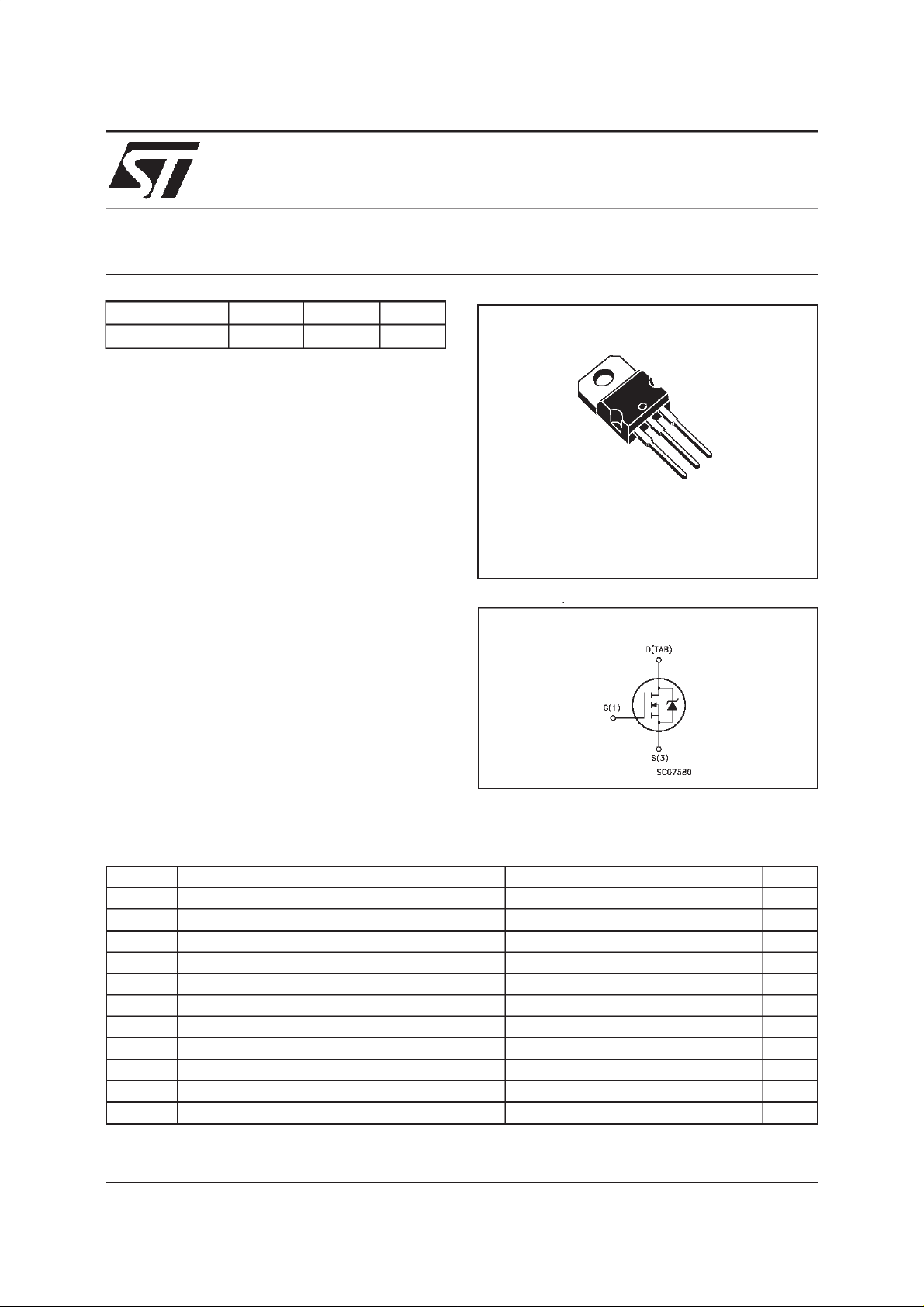
- 80A TO-220
STripFET POWER MOSFET
PRELIMINARY DATA
3
2
1
TO-220
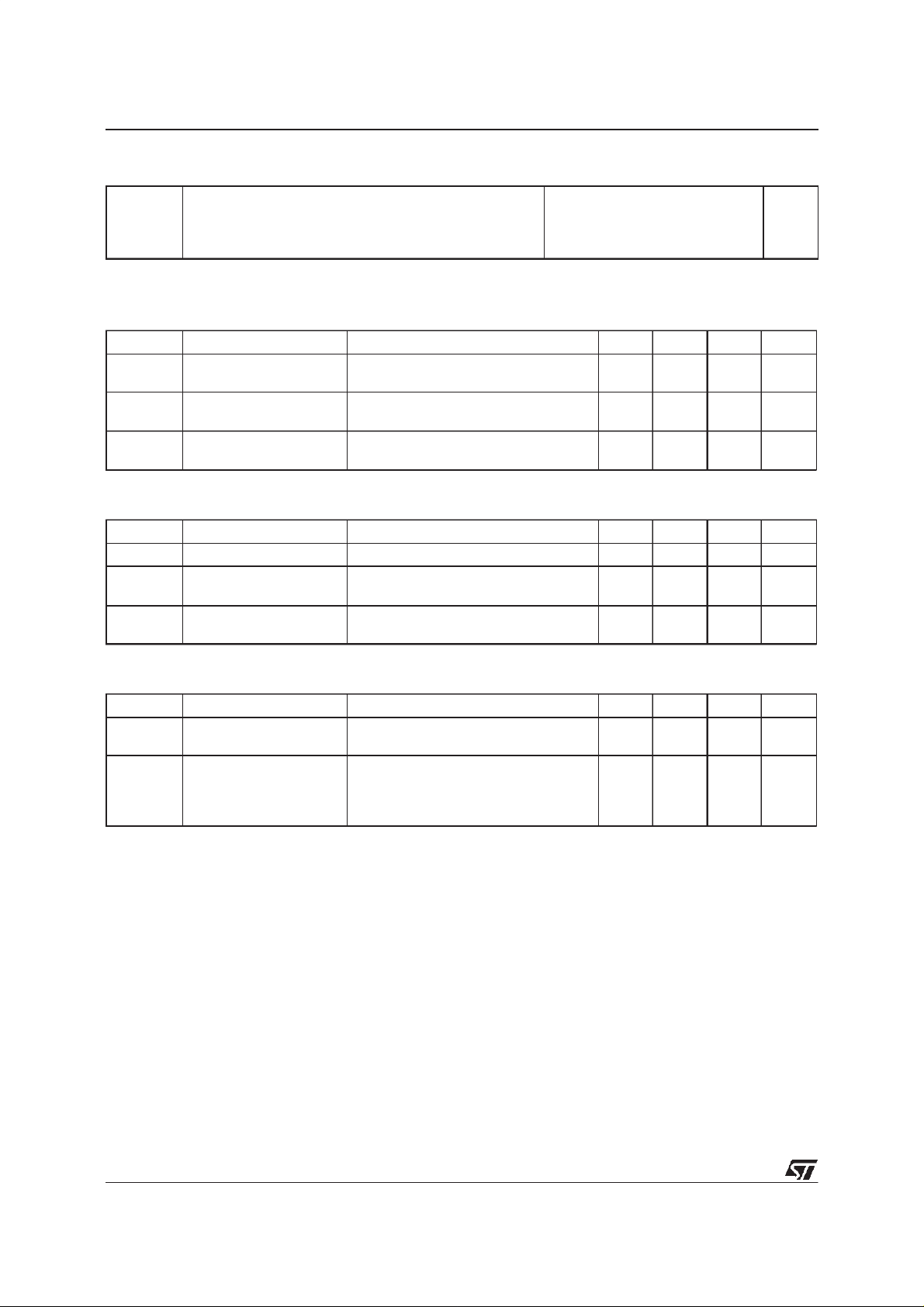
INTERNAL SCHEMATIC DIAGRAM
ABSOLUTE MAXIMUM RATINGS
Symbol Parameter Value Uni t
V
V
V
I
D
I
DM
P
E
AS
T
(•) Pulsewidth limited by safe operating area (••) Current limited by package (1) starting Tj
November 1999
Dra in- sour c e Voltage (VGS=0) 30 V
DS
Drain- gate Voltage (RGS=20kΩ)30V
DGR
Gate-s ource Voltage ± 20 V
GS
(••) Dra in Curr ent (c ont i nuous) at Tc=25oC80A
Dra in Curr ent (c ont i nuous) at Tc= 100oC56A
I
D
(
Dra in Curr ent (puls e d) 320 A
•)
Tot al Dissipatio n a t Tc=25oC 210 W
tot
Der ati ng Fa ct or 1.43 W/
o
C
(1) Single Pulse Avalanche En er gy 2 J
St orage T e m pe ra t ure -65 to 175
stg
Max. Oper at ing Junct ion Temperat ur e 175
T
j
=25oC,ID=40A , VDD=15V
o
C
o
C
1/6
Page 2
STP80NF03L-04
THERMAL DATA
R
thj-case
Rthj-amb
R
thc-sink
T
Ther mal Resistanc e Junct ion-case Max
Ther mal Resistanc e Junct ion-ambient Max
Ther mal Resistanc e Case-sink Ty p
Maximum Lead Temperat ur e For S o ldering Pur p os e
l
0.7
62.5
0.5
300
o
C/W
oC/W
o
C/W
o
C
ELECTRICAL CHARACTERISTICS
=25oC unless otherwisespecified)
(T
case
OFF
Symbol Parameter Test Conditions Min. Typ. Max. Unit
V
(BR)DSS
Drain-source
ID=250µAVGS=0 30 V
Break dow n Volt age
I
DSS
I
GSS
Zero Gate Voltage
Drain Current (V
GS
Gat e- bod y L eak ag e
Current (V
DS
=0)
=0)
V
=MaxRating
DS
=MaxRating Tc=125oC
V
DS
V
= ± 20 V ± 100 nA
GS
1
10
ON(∗)
Symbol Parameter Test Conditions Min. Typ. Max. Unit
V
GS(th)
R
DS(on)
I
D(on)
Gate Threshold Voltage VDS=VGSID= 250 µ A11.72.5V
Sta t ic Drain -s ource O n
Resistance
VGS=10V ID=40A
=4.5V ID=40A
V
GS
On State Drain Current VDS>I
D(on)xRDS(on)max
0.0034
0.0042
80 A
0.004
0.0055ΩΩ
VGS=10V
DYNAMIC
Symbol Parameter Test Conditions Min. Typ. Max. Unit
g
(∗)Forward
fs
Tr ansc on duc tance
C
C
C
Input C apaci t anc e
iss
Out put Capacit anc e
oss
Reverse Tr ansfer
rss
Capacit a nc e
VDS>I
D(on)xRDS(on)maxID
=15 A 50 S
VDS=25V f=1MHz VGS= 0 7000
1700
600
µ
µA
pF
pF
pF
A
2/6
Page 3

STP80NF03L-04
ELECTRICAL CHARACTERISTICS
(continued)
SWITCHING ON
Symbol Parameter Test Conditions Min. Typ. Max. Unit
t
d(on)
Tur n-on Delay T ime
Rise Ti m e
t
r
VDD=15V ID=40A
R
=4.7
G
Ω
VGS=4.5V
50
275
(Resis t iv e Loa d, see fig. 3)
Q
Q
Q
Tot al G at e Charge
g
Gat e- Source Charge
gs
Gate-Drain Charge
gd
VDD=24V ID=80A VGS= 4.5 V 120
37
58
160 nC
SWITCHING OFF
Symbol Parameter Test Conditions Min. Typ. Max. Unit
t
d(off)
Tur n-of f D ela y Time
t
Fall T ime
f
VDD=15V ID=40A
=4.7 Ω VGS=4.5V
R
G
230
190
(Resis t iv e Loa d, see fig. 3)
t
r(Voff)
t
t
Off-voltage Ris e Time
Fall T ime
f
Cross-over T ime
c
V
=24V ID=80A
clamp
=4.7 Ω VGS=4.5V
R
G
(Indu ct iv e Load, see fig . 5)
175
280
470
SOURCEDRAINDIODE
Symbol Parameter Test Conditions Min. Typ. Max. Unit
I
SDM
V
I
SD
Q
I
RRM
SD
t
Source-drain Current
(•)
Source-drain Current
80
320
(pulsed)
(∗)ForwardOnVoltage ISD=80A VGS=0 1.5 V
Reverse Recover y
rr
Time
Reverse Recover y
rr
ISD= 80 A di/dt = 100 A/µs
=20V Tj=150oC
V
DD
(see test circuit, fig. 5)
88
0.176
Charge
Reverse Recover y
4.4
Current
ns
ns
nC
nC
ns
ns
ns
ns
ns
A
A
ns
µC
A
(∗) Pulsed:Pulse duration = 300 µs, duty cycle 1.5 %
(•) Pulse width limited by safe operatingarea
3/6
Page 4

STP80NF03L-04
Fig. 1:
UnclampedInductiveLoad Test Circuit
Fig. 3: SwitchingTimes Test Circuits For
ResistiveLoad
Fig. 2:
UnclampedInductive Waveform
Fig. 4: Gate Chargetest Circuit
Fig. 5:
Test CircuitFor InductiveLoad Switching
And Diode Recovery Times
4/6
Page 5

TO-220 MECHANICAL DATA
STP80NF03L-04
DIM.
MIN. TYP. MAX. MIN. TYP. MAX.
A 4.40 4.60 0.173 0.181
C 1.23 1.32 0.048 0.051
D 2.40 2.72 0.094 0.107
D1 1.27 0.050
E 0.49 0.70 0.019 0.027
F 0.61 0.88 0.024 0.034
F1 1.14 1.70 0.044 0.067
F2 1.14 1.70 0.044 0.067
G 4.95 5.15 0.194 0.203
G1 2.4 2.7 0.094 0.106
H2 10.0 10.40 0.393 0.409
L2 16.4 0.645
L4 13.0 14.0 0.511 0.551
L5 2.65 2.95 0.104 0.116
L6 15.25 15.75 0.600 0.620
L7 6.2 6.6 0.244 0.260
L9 3.5 3.93 0.137 0.154
DIA. 3.75 3.85 0.147 0.151
mm inch
E
A
L4
D
F2
F1
G1
H2
G
F
P011C
C
D1
L2
Dia.
L5
L7
L6
L9
5/6
Page 6

STP80NF03L-04
Information furnishedis believedto be accurate and reliable.However, STMicroelectronics assumes no responsibilityfor the consequences
of use of such information nor for any infringement of patents or other rights of third parties which may result from its use. No licenseis
granted by implication or otherwise under any patent or patent rights of STMicroelectronics. Specificationmentioned in this publication are
subjecttochange without notice.This publication supersedesand replaces all information previouslysupplied. STMicroelectronicsproducts
are not authorized for use as critical components in lifesupport devices or systems without express written approval of STMicroelectronics.
The STlogo is a trademark of STMicroelectronics
1999 STMicroelectronics – Printed in Italy – All Rights Reserved
STMicroelectronics GROUP OF COMPANIES
Australia - Brazil - China - Finland - France - Germany - Hong Kong - India - Italy - Japan - Malaysia - Malta - Morocco -
6/6
Singapore - Spain - Sweden - Switzerland - United Kingdom - U.S.A.
http://www.st.com
.
 Loading...