

Page 1
STP80NE06-10
N - CHANNEL ENHANCEMENT MODE
” SINGLE FEATURE SIZE ” POWER MOSFET
TYPE V
DSS
R
DS(on)
I
D
STP80 NE 0 6- 1 0 60 V <0. 01 Ω 80 A
■ TYPICALR
■ EXCEPTIONAL dv/dt CAPABILITY
■ 100% AVALANCHETESTED
■ APPLICATIONORIENTED
DS(on)
=0.0085 Ω
CHARACTERIZATION
DESCRIPTION
This Power MOSFET is the latestdevelopmentof
SGS-THOMSON unique ”Single Feature Size”
strip-based process. The resulting transistor
shows extremely high packing density for low
on-resistance, rugged avalanche characteristics
and less critical alignment steps therefore a
remarkablemanufacturingreproducibility.
APPLICATIONS
■ SOLENOIDANDRELAY DRIVERS
■ MOTORCONTROL, AUDIOAMPLIFIERS
■ DC-DCCONVERTERS
■ AUTOMOTIVE ENVIRONMENT
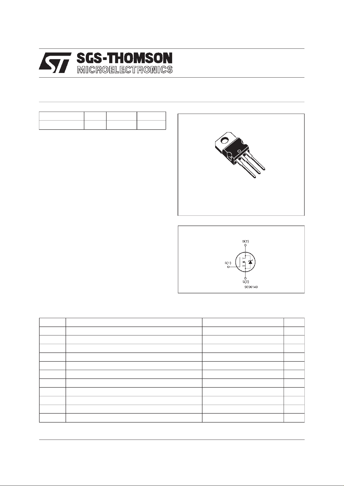
3
2
1
TO-220
INTERNAL SCHEMATIC DIAGRAM
ABSOLUTE MAXIMUM RATINGS
Symb o l Para meter Value Uni t
V
V
V
I
DM
P
dv/ dt Peak Diode Recov ery vo lt age sl ope 7 V/ns
T
(•) Pulsewidth limitedby safe operating area (1)ISD≤ 80 A,di/dt ≤ 300 A/µs, VDD≤ V
February 1998
Drain-source Voltage (VGS=0) 60 V
DS
Drain- gate Voltage (RGS=20kΩ)
DGR
Gat e- source Volt age ± 20 V
GS
I
Drain Current (c on t in uous) at Tc=25oC80A
D
I
Drain Current (c on t in uous) at Tc=100oC57A
D
60 V
(•) Drain Current (pul sed) 320 A
Tot al Dissip at i on at Tc=25oC150W
tot
Derat in g F actor 1 W/
Sto rage Temperature -65 to 175
stg
T
Max. Oper at in g Junc t io n Temperature 175
j
(BR)DSS,Tj≤TJMAX
o
C
o
C
o
C
1/8
Page 2
STP80NE06-10
THERMAL DATA
R
thj-case
Rthj-amb
R
thc-sin k
T
AVALANCHE CHARACTERISTICS
Symbol Para met e r Max Valu e Unit
I
AR
E
Ther mal Resistan ce J unction-c a s e Max
Ther mal Resistan ce J unction-ambient Max
Ther mal Resistan ce Cas e - sink Ty p
Maximum Lead T e mperat u re For Solderi ng P ur p ose
l
Avalanche Curre nt , Rep et it i v e or Not-Repetitive
(pulse width limited by T
Single Pulse Avalanche Energy
AS
(starting T
=25oC, ID=IAR,VDD=30V)
j
max, δ <1%)
j
1
62.5
0.5
300
80 A
250 mJ
o
C/W
oC/W
o
C/W
o
C
ELECTRICAL CHARACTERISTICS (T
=25oC unlessotherwisespecified)
case
OFF
Symbol Parameter Test Conditions Min. Typ. Max. Unit
V
(BR)DSS
Drain-source
=250µAVGS=0
I
D
60 V
Breakdown Voltage
I
DSS
I
GSS
Zer o Gate V o lt age
Drain Cur re nt (V
GS
Gat e-body Leakage
Current (V
DS
=0)
=0)
=MaxRating
V
DS
V
=MaxRating Tc=125
DS
o
C
= ± 20 V
V
GS
1
10
± 100 nA
ON (∗)
Symbol Parameter Test Conditions Min. Typ. Max. Unit
V
GS(th )
Gate Threshold
V
DS=VGSID
=250µA
234V
Voltage
R
DS(on)
Stati c Drain-so urce On
VGS=10V ID=40A 8.5 10 mΩ
Resistance
I
D(on)
On State Drain Cu r rent VDS>I
D(on)xRDS(on)max
80 A
VGS=10V
DYNAMIC
Symbol Parameter Test Conditions Min. Typ. Max. Unit
g
(∗)Forward
fs
Tr ansconductance
C
C
C
Input Capaci t ance
iss
Out put Capacitance
oss
Reverse Transfer
rss
Capa cit an c e
VDS>I
D(on)xRDS(on)maxID
=40 A 19 3 8 S
VDS=25V f=1MHz VGS= 0 7600
890
150
10000
1100
200
µA
µA
pF
pF
pF
2/8
Page 3

STP80NE06-10
ELECTRICAL CHARACTERISTICS (continued)
SWITCHINGON
Symbol Parameter Test Conditions Min. Typ. Max. Unit
t
d(on)
t
r
Turn-on Time
Rise Tim e
VDD=30V ID=40A
=4.7 Ω VGS=10V
R
G
(see test circuit, figure 3)
Q
Q
Q
Total Gate Charge
g
Gat e-Sourc e Charge
gs
Gate-Drain Charge
gd
VDD=48V ID=80A VGS= 10 V 140
SWITCHINGOFF
Symbol Parameter Test Conditions Min. Typ. Max. Unit
t
r(Voff)
t
Of f - voltage Rise Time
t
Fall Time
f
Cross-over Time
c
VDD=48V ID=40A
=4.7 Ω VGS=10V
R
G
(see test circuit, figure 5)
SOURCE DRAIN DIODE
Symbol Parameter Test Conditions Min. Typ. Max. Unit
I
SD
I
SDM
V
SD
t
Q
I
RRM
(∗) Pulsed: Pulse duration =300 µs, duty cycle 1.5 %
(•) Pulse width limited by safe operating area
Source-drain Current
(•)
Source-drain Current
(pulsed)
(∗) For ward On Voltage ISD=80A VGS=0 1.5 V
Reverse Recover y
rr
Time
Reverse Recover y
rr
= 80 A di/ dt = 100 A/µs
I
SD
=30V Tj=150oC
V
DD
(see test circuit, figure 5)
Charge
Reverse Recover y
Current
50
15065200
20
50
45
75
130
60
100
170
80
320
100
0.4
8
ns
ns
nC
nC
nC
ns
ns
ns
A
A
ns
µC
A
Safe Operating Areafor ThermalImpedance
3/8
Page 4

STP80NE06-10
OutputCharacteristics
Transconductance
TransferCharacteristics
StaticDrain-sourceOn Resistance
GateCharge vs Gate-sourceVoltage
4/8
CapacitanceVariations
Page 5

STP80NE06-10
Normalized Gate Threshold Voltage vs
Temperature
Source-drainDiode Forward Characteristics
Normalized On Resistancevs Temperature
5/8
Page 6

STP80NE06-10
Fig. 1: Unclamped Inductive Load TestCircuit
Fig. 3: SwitchingTimes Test Circuits For
ResistiveLoad
Fig. 2: Unclamped Inductive Waveform
Fig. 4: Gate Chargetest Circuit
Fig. 5: Test Circuit For InductiveLoad Switching
And Diode RecoveryTimes
6/8
Page 7

TO-220 MECHANICAL DATA
STP80NE06-10
DIM.
MIN. TYP. MAX. MIN. TYP. MAX.
A 4.40 4.60 0.173 0.181
C 1.23 1.32 0.048 0.051
D 2.40 2.72 0.094 0.107
D1 1.27 0.050
E 0.49 0.70 0.019 0.027
F 0.61 0.88 0.024 0.034
F1 1.14 1.70 0.044 0.067
F2 1.14 1.70 0.044 0.067
G 4.95 5.15 0.194 0.203
G1 2.4 2.7 0.094 0.106
H2 10.0 10.40 0.393 0.409
L2 16.4 0.645
L4 13.0 14.0 0.511 0.551
L5 2.65 2.95 0.104 0.116
L6 15.25 15.75 0.600 0.620
L7 6.2 6.6 0.244 0.260
L9 3.5 3.93 0.137 0.154
DIA. 3.75 3.85 0.147 0.151
mm inch
E
A
L4
D
F2
F1
G1
F
H2
G
C
D1
L2
Dia.
L5
L7
L6
L9
P011C
7/8
Page 8

STP80NE06-10
Information furnished is believed to be accurate and reliable. However, SGS-THOMSON Microelectronics assumes no responsability for the
consequences of use of such information nor for any infringement of patents or other rightsof third parties which may results from its use. No
license is granted by implication or otherwise under any patent orpatent rights of SGS-THOMSON Microelectronics. Specifications mentioned
in thispublication are subject to change without notice. This publication supersedes and replaces all information previously supplied.
SGS-THOMSON Microelectronics products are not authorizedfor useas criticalcomponents in life support devices orsystems withoutexpress
written approval ofSGS-THOMSON Microelectonics.
1998 SGS-THOMSON Microelectronics - Printed in Italy -All Rights Reserved
Australia - Brazil - Canada -China - France - Germany - Italy - Japan - Korea - Malaysia - Malta - Morocco - The Netherlands -
Singapore - Spain - Sweden- Switzerland - Taiwan - Thailand - United Kingdom -U.S.A
8/8
SGS-THOMSON Microelectronics GROUP OF COMPANIES
...
 Loading...