

Page 1
STP80NE03L-06
N - CHANNEL ENHANCEMENT MODE
” SINGLE FEATURE SIZE ” POWER MOSFET
TYPE V
DSS
R
DS(on)
I
D
ST P80NE03L- 06 30 V < 0.006 Ω 80 A
■ TYPICALR
■ EXCEPTIONALdv/dtCAPABILITY
■ 100%AVALANCHETESTED
■ LOW GATE CHARGE 100
■ APPLICATIONORIENTED
DS(on)
= 0.005 Ω
o
C
CHARACTERIZATION
DESCRIPTION
This Power Mosfet is the latest development of
STMicroelectronics unique ”Single Feature
Size” strip-based process. The resulting
transistor shows extremely high packing density
for low on-resistance, rugged avalance
characteristics and less critical alignment steps
therefore a remarkable manufacturing
reproducibility.
APPLICATIONS
■ HIGHCURRENT, HIGH SPEED SWITCHING
■ SOLENOIDAND RELAY DRIVERS
■ MOTORCONTROL, AUDIOAMPLIFIERS
■ DC-DC& DC-ACCONVERTERS
■ AUTOMOTIVEENVIRONMENT(INJECTION,
ABS, AIR-BAG, LAMPDRIVERS,Etc. )
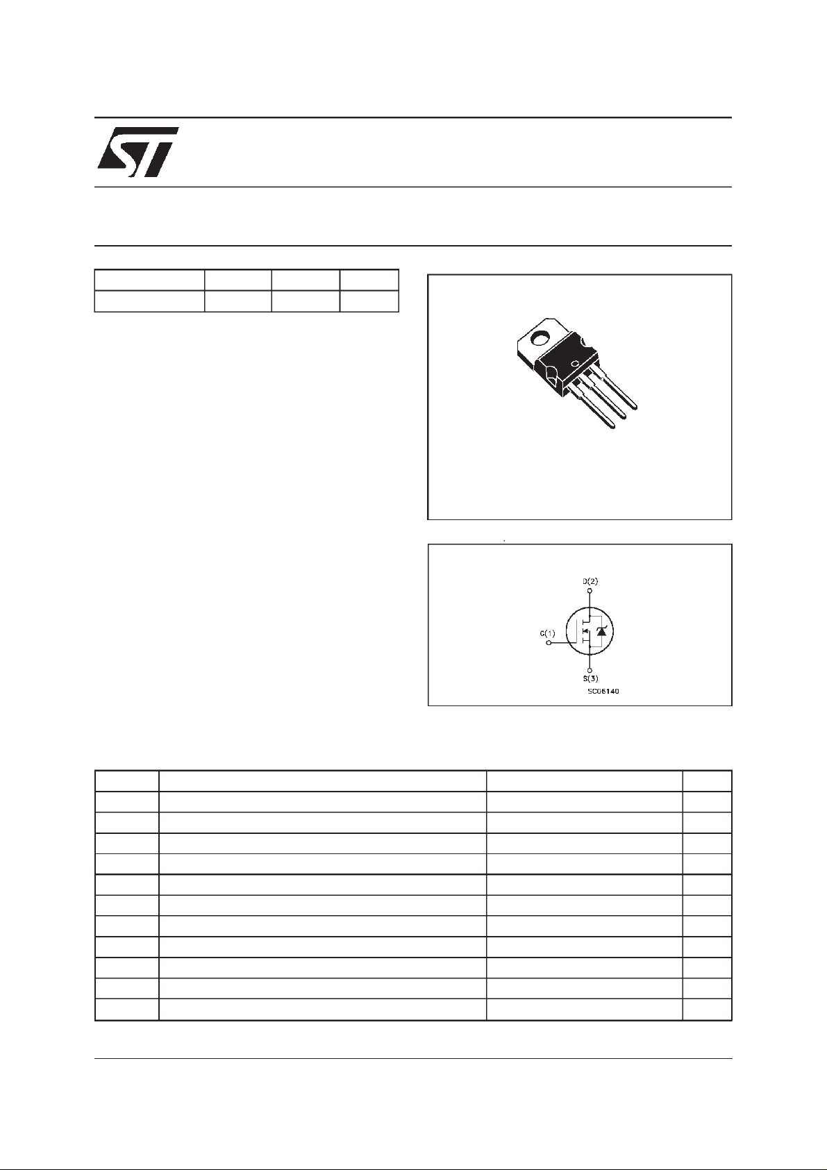
3
2
1
TO-220
INTERNAL SCHEMATIC DIAGRAM
ABSOLUTE MAXIMUM RATINGS
Symbol Parameter Value Unit
V
V
V
I
DM
P
dv/ dt Peak Diode Recovery voltage sl ope 7 V/ ns
T
(•) Pulse width limited by safe operating area (1)ISD≤ 80 A, di/dt ≤ 300 A/µs, VDD≤ V
February 2000
Dra in- sour c e Volt age (VGS=0) 30 V
DS
Dra in- gat e Voltage (RGS=20kΩ)30V
DGR
Gat e-source Voltage ± 22 V
GS
I
Dra in Cu rr ent ( c ont inuous) at Tc=25oC80A
D
I
Dra in Cu rr ent ( c ont inuous) at Tc=100oC60A
D
(•) D rain Current ( p uls ed ) 320 A
Tot al Dis s ipation at Tc=25oC 150 W
tot
Derating Factor 1 W/
St orage Temper at ure -65 to 175
stg
T
Max. Operating Junc t ion Temperat ur e 175
j
(BR)DSS,Tj≤TJMAX
o
C
o
C
o
C
1/8
Page 2
STP80NE03L-06
THERMAL DATA
R
thj-case
Rthj-a mb
R
thc-sink
T
AVALANCHE CHARACTERISTICS
Symbol Parameter Max V alue Unit
I
AR
E
Ther mal Resistanc e Junct ion-case Max
Ther mal Resistanc e Junct ion-ambient Max
Ther mal Resistanc e Case-sink Ty p
Maximum Lead T e mperature For Soldering P urp os e
l
Avalanche Current, Repetitive or Not-Repetitive
(pulse width limited by T
Single Pul se Avalanc he E nergy
AS
(starting T
=25oC, ID=IAR,VDD=15V)
j
max,δ <1%)
j
1
62.5
0.5
300
80 A
600 mJ
o
C/W
oC/W
o
C/W
o
C
ELECTRICAL CHARACTERISTICS
=25oC unless otherwisespecified)
(T
case
OFF
Symbol Parameter Test Conditions Min. Typ. Max. U nit
V
(BR)DSS
Drain-source
ID=250µAVGS=0 30 V
Break dow n Vo lt age
I
DSS
I
GSS
Zero Gate Voltage
Drain Curre nt (V
GS
Gat e- bod y Leakag e
Current (V
DS
=0)
=0)
V
=MaxRating
DS
=MaxRating Tc=125oC
V
DS
V
=± 15 V
GS
1
10
100 nA
±
ON(∗)
Symbol Parameter Test Conditions Min. Typ. Max. U nit
V
GS(th)
R
DS(on)
I
D(on)
Gate Threshold Voltage VDS=VGSID= 250 µ A11.72.5V
Sta t ic Drain-s our c e On
Resistance
VGS=10V ID=40A
=5V ID=40A
V
GS
On StateDrain Current VDS>I
D(on)xRDS(on)ma x
0.005 0.006
0.009
80 A
VGS=10V
DYNAMIC
Symbol Parameter Test Conditions Min. Typ. Max. U nit
g
(∗)Forward
fs
Tr ansc on duc tance
C
C
C
Input Capaci t ance
iss
Out put Capac itance
oss
Reverse Transfer
rss
Capacit a nc e
VDS>I
D(on)xRDS(on)ma xID
=40 A 30 50 S
VDS=25V f=1MHz VGS= 0 6500
1500
500
8700
2000
700
µ
µA
Ω
pF
pF
pF
A
2/8
Page 3
STP80NE03L-06
ELECTRICAL CHARACTERISTICS
(continued)
SWITCHINGON
Symbol Parameter Test Conditions Min. Typ. Max. U nit
t
d(on)
t
r
Turn-on Time
Rise Time
VDD=15V ID=40A
R
G
=4.7
Ω
VGS=5V
40
26055350
(see test circuit, figure 3)
Q
Q
Q
Tot al Gate C harge
g
Gat e- Source Charge
gs
Gate-Drain Charge
gd
VDD=24V ID=80A VGS=5V 95
30
44
130 nC
SWITCHINGOFF
Symbol Parameter Test Conditions Min. Typ. Max. U nit
t
r(Voff)
t
t
Off-voltage Ris e Time
Fall T ime
f
Cross-over Time
c
VDD=24V ID=80A
=4.7 Ω VGS=5V
R
G
(see test circuit, figure 5)
70
165
250
95
220
340
SOURCEDRAINDIODE
Symbol Parameter Test Conditions Min. Typ. Max. U nit
I
SD
I
SDM
V
SD
t
Q
I
RRM
(∗) Pulsed:Pulse duration = 300µs, duty cycle 1.5%
(•) Pulse width limited by safeoperating area
Source-drain Current
(•)
Source-drain Current
80
320
(pulsed)
(∗)ForwardOnVoltage ISD=80A VGS=0 1.5 V
Reverse Recovery
rr
Time
Reverse Recovery
rr
ISD= 80 A di/dt = 100 A/µs
=15V Tj= 150oC
V
DD
(see test circuit, figure 5)
75
0.14
Charge
Reverse Recovery
4
Current
ns
ns
nC
nC
ns
ns
ns
A
A
ns
µ
A
C
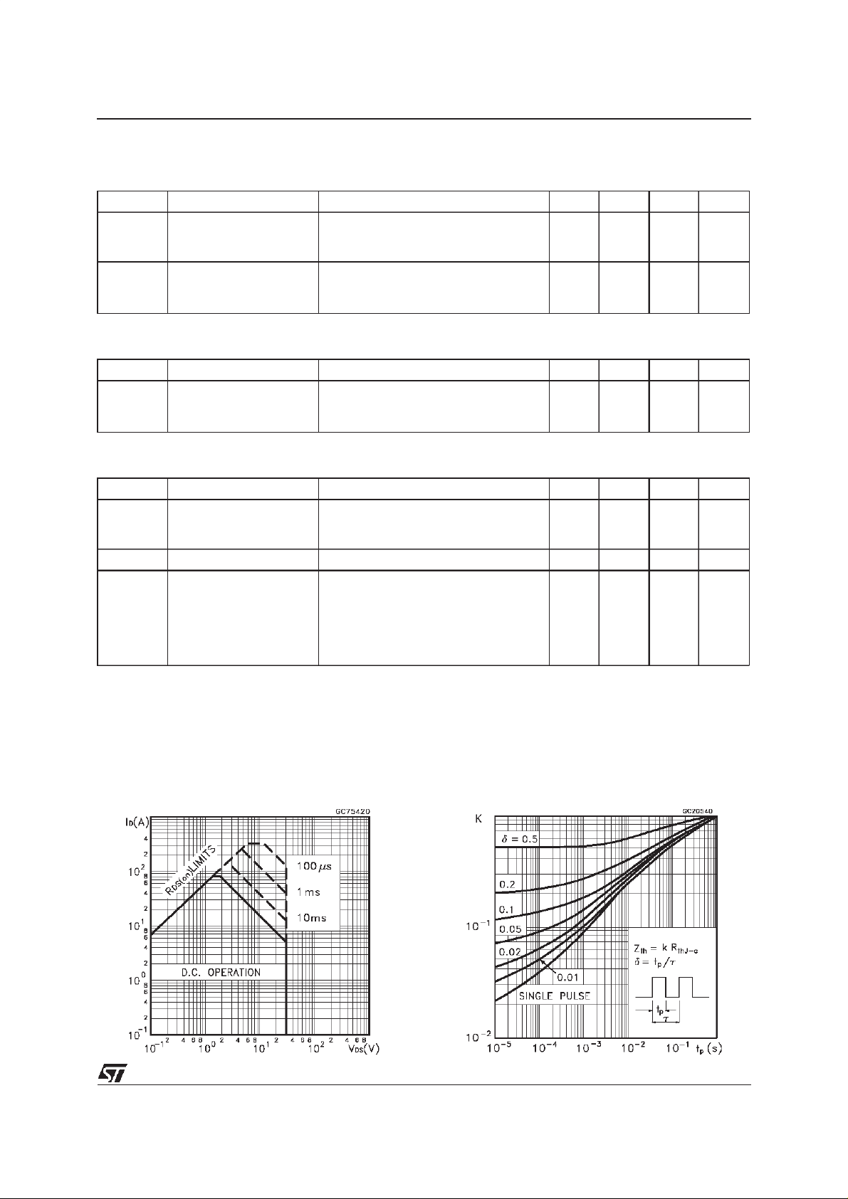
SafeOperating Area for ThermalImpedance
3/8
Page 4

STP80NE03L-06
OutputCharacteristics
Transconductance
TransferCharacteristics
Static Drain-sourceOn Resistance
Gate Charge vs Gate-sourceVoltage
4/8
CapacitanceVariations
Page 5

STP80NE03L-06
NormalizedGate ThresholdVoltage vs
Temperature
Source-drainDiode ForwardCharacteristics
NormalizedOn Resistancevs Temperature
5/8
Page 6

STP80NE03L-06
Fig. 1:
UnclampedInductiveLoad Test Circuit
Fig. 3: SwitchingTimes Test CircuitsFor
ResistiveLoad
Fig. 2:
UnclampedInductive Waveform
Fig. 4: Gate Charge test Circuit
Fig. 5:
Test CircuitFor InductiveLoad Switching
And Diode Recovery Times
6/8
Page 7

TO-220 MECHANICALDATA
STP80NE03L-06
DIM.
MIN. TYP. MAX. MIN. TYP. MAX.
A 4.40 4.60 0.173 0.181
C 1.23 1.32 0.048 0.051
D 2.40 2.72 0.094 0.107
D1 1.27 0.050
E 0.49 0.70 0.019 0.027
F 0.61 0.88 0.024 0.034
F1 1.14 1.70 0.044 0.067
F2 1.14 1.70 0.044 0.067
G 4.95 5.15 0.194 0.203
G1 2.4 2.7 0.094 0.106
H2 10.0 10.40 0.393 0.409
L2 16.4 0.645
L4 13.0 14.0 0.511 0.551
L5 2.65 2.95 0.104 0.116
L6 15.25 15.75 0.600 0.620
L7 6.2 6.6 0.244 0.260
L9 3.5 3.93 0.137 0.154
DIA. 3.75 3.85 0.147 0.151
mm inch
E
A
L4
D
F2
F1
G1
H2
G
F
P011C
C
D1
L2
Dia.
L5
L7
L6
L9
7/8
Page 8

STP80NE03L-06
Information furnished is believed tobeaccurateand reliable.However, STMicroelectronics assumes no responsibility for the consequences
of use of such information nor for any infringement of patents or other rights of third parties which may result from its use. No license is
granted by implication or otherwise under any patent or patent rights of STMicroelectronics. Specificationmentioned in this publicationare
subjecttochange without notice.This publication supersedes andreplaces all information previouslysupplied.STMicroelectronics products
are not authorized for use as critical components in life support devicesor systemswithout express written approval of STMicroelectronics.
The STlogo is a trademark ofSTMicroelectronics
1999STMicroelectronics – Printedin Italy – All Rights Reserved
STMicroelectronics GROUP OF COMPANIES
Australia - Brazil - China - Finland - France - Germany - Hong Kong - India - Italy- Japan - Malaysia - Malta - Morocco -
8/8
Singapore - Spain - Sweden - Switzerland - United Kingdom - U.S.A.
http://www.st.com
.
 Loading...