

Page 1
N - CHANNEL ENHANCEMENT MODE
” SINGLE FEATURE SIZE ” POWER MOSFET
TYPE V
DSS
STP80NE03L-06 30 V < 0.006 Ω 80 A
■ TYPICALR
■ EXCEPTIONAL dv/dt CAPABILITY
■ 100% AVALANCHETESTED
■ LOW GATE CHARGE 100
■ APPLICATIONORIENTED
DS(on)
=0.005 Ω
CHARACTERIZATION
DESCRIPTION
This Power Mosfet is the latest development of
SGS-THOMSON unique ”Single Feature Size”
strip-based process. The resulting transistor
shows extremely high packing density for low onresistance, rugged avalance characteristics and
less critical alignment steps therefore a remarkable manufacturingreproducibility.
APPLICATIONS
■ HIGH CURRENT, HIGHSPEEDSWITCHING
■ SOLENOIDANDRELAY DRIVERS
■ MOTORCONTROL, AUDIO AMPLIFIERS
■ DC-DC& DC-AC CONVERTERS
■ AUTOMOTIVE ENVIRONMENT(INJECTION,
ABS, AIR-BAG, LAMPDRIVERS,Etc. )
o
R
C
DS(on)
I
D
STP80NE03L-06
PRELIMINARY DATA
3
2
1
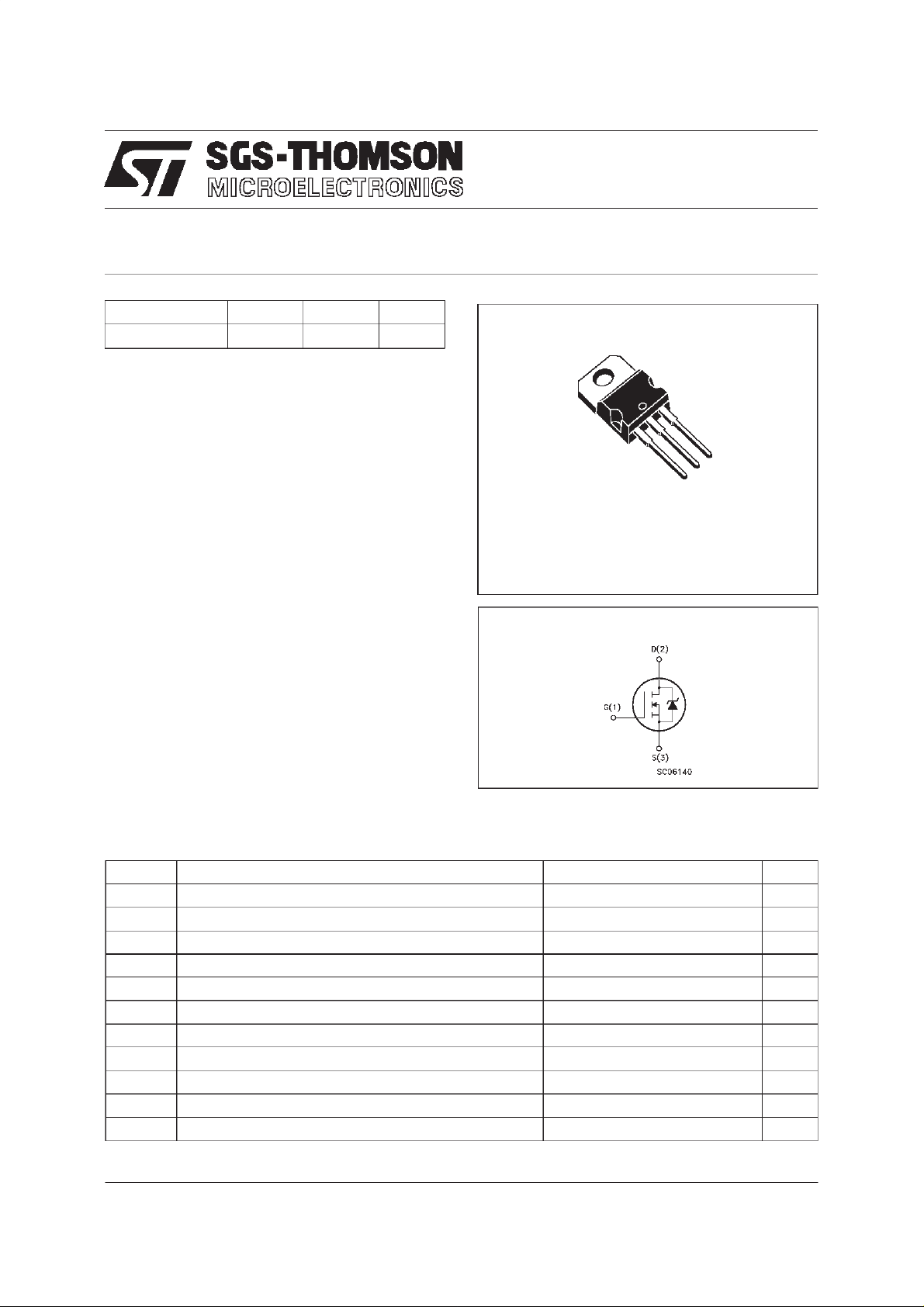
TO-220
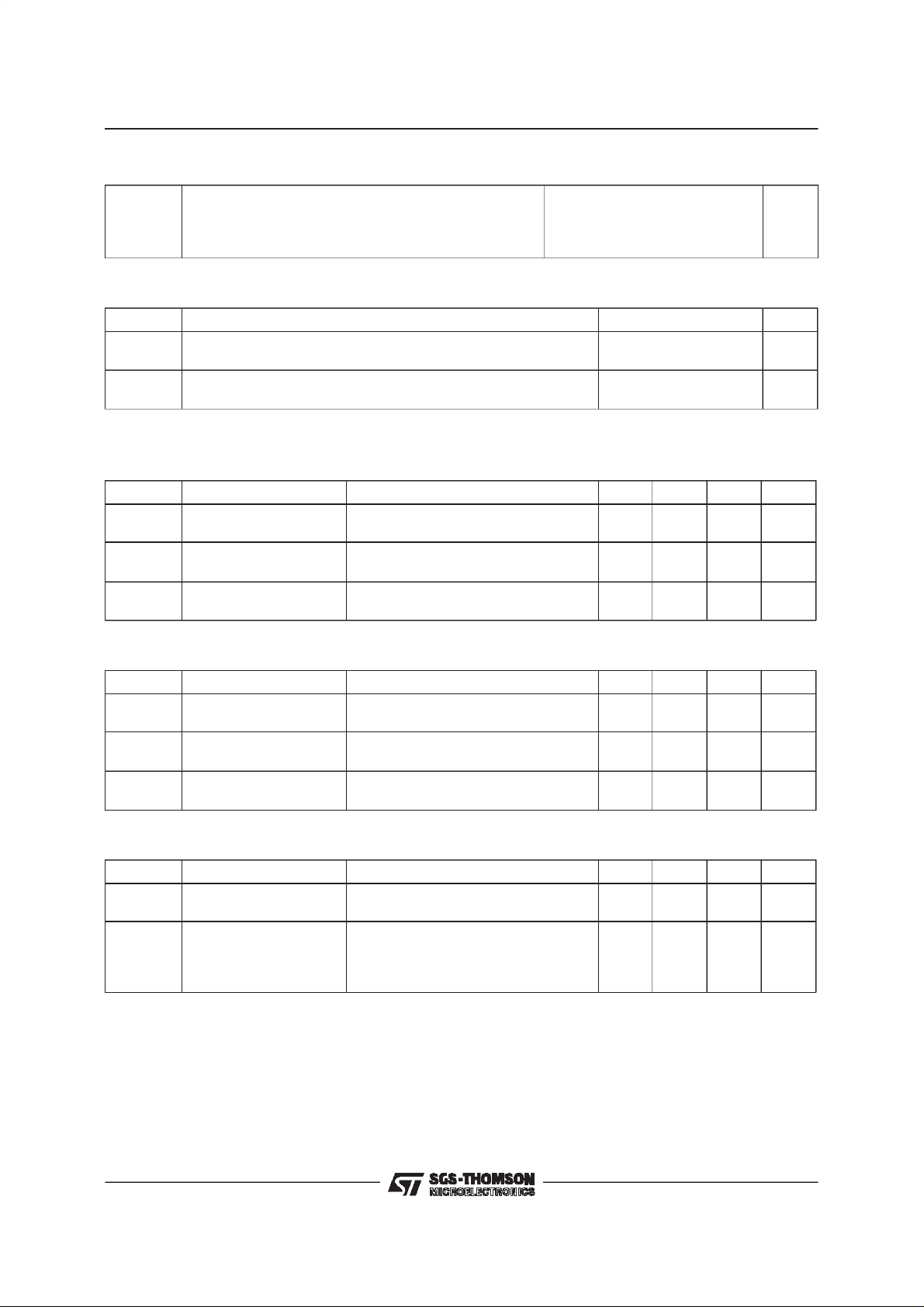
INTERNAL SCHEMATIC DIAGRAM
ABSOLUTE MAXIMUM RATINGS
Symb o l Para meter Value Uni t
V
V
V
I
DM
P
dv/ dt Peak Diode Recov ery vo lt age sl ope 7 V/ns
T
(•) Pulsewidth limitedby safe operating area (1)ISD≤ 80 A,di/dt ≤ 300 A/µs, VDD≤ V
December 1997
Drain-source Voltage (VGS=0) 30 V
DS
Drain- gate Voltage (RGS=20kΩ)
DGR
Gat e- source Volt age ± 15 V
GS
I
Drain Current (c on t in uous) at Tc=25oC80A
D
I
Drain Current (c on t in uous) at Tc=100oC60A
D
30 V
(•) Drain Current (pulsed) 320 A
Tot al Dissip at i on at Tc=25oC150W
tot
Derat in g F actor 1 W/
Sto rage Temperature -65 to 175
stg
T
Max. Oper at in g Junc t io n Temperature 175
j
(BR)DSS,Tj≤TJMAX
o
C
o
C
o
C
1/6
Page 2
STP80NE03L-06
THERMAL DATA
R
thj-case
Rthj-amb
R
thc-sin k
T
AVALANCHE CHARACTERISTICS
Symbol Para met e r Max Va lu e Uni t
I
AR
E
Ther mal Resist an c e Junct io n- ca s e Max
Ther mal Resist an c e Junct io n- ambient Max
Ther mal Resist an c e Case-sink Ty p
Maximum Lead T emperature Fo r S oldering Purpose
l
Avalanche Curre nt , Rep et it i v e or Not- Re petitive
(pulse width limited by T
Single Pulse Avalanche Energy
AS
(starting T
=25oC, ID=IAR,VDD=15V)
j
max, δ <1%)
j
1
62.5
0.5
300
80 A
600 mJ
o
C/W
oC/W
o
C/W
o
C
ELECTRICAL CHARACTERISTICS (T
=25oC unlessotherwise specified)
case
OFF
Symbol Parameter Test Cond ition s Min. Typ. Max. Un it
V
(BR)DSS
Drain-source
=250µAVGS=0
I
D
30 V
Breakdown Voltage
I
DSS
I
GSS
Zer o Gate Vo lt age
Drain Cur re nt (V
GS
Gat e-body Le akage
Current (V
DS
=0)
=0)
=MaxRating
V
DS
V
=MaxRating Tc=125oC
DS
= ± 15 V
V
GS
1
10
± 100 nA
ON (∗)
Symbol Parameter Test Cond ition s Min. Typ. Max. Un it
V
GS(th )
Gate Threshold
V
DS=VGSID
=250µA
11.72.5V
Voltage
R
DS(on)
I
D(on)
Stati c D rain-source On
Resistance
VGS=10V ID=40A
=5V ID=40A
V
GS
On St at e D rain Cu r rent VDS>I
D(on)xRDS(on)max
0.005 0. 006
0.009
80 A
VGS=10V
DYNAMIC
Symbol Parameter Test Cond ition s Min. Typ. Max. Un it
g
(∗)Forward
fs
Tr ansconductance
C
C
C
Input Capaci t ance
iss
Out put C apa citance
oss
Reverse T rans fer
rss
Capa cit an c e
VDS>I
D(on)xRDS(on)maxID
=40 A 30 50 S
VDS=25V f=1MHz VGS= 0 6500
1500
500
8700
2000
700
µA
µA
Ω
pF
pF
pF
2/6
Page 3

STP80NE03L-06
ELECTRICAL CHARACTERISTICS (continued)
SWITCHINGON
Symbol Parameter Test Cond ition s Min. Typ. Max. Un it
t
d(on)
t
r
Turn-on T ime
Rise Tim e
VDD=15V ID=40A
=4.7 Ω VGS=5V
R
G
(see test circuit, figure 3)
Q
Q
Q
Total Gate Charge
g
Gat e-Sourc e Charge
gs
Gate-Drain Charge
gd
VDD=24V ID=80A VGS=5V 95
SWITCHINGOFF
Symbol Parameter Test Cond ition s Min. Typ. Max. Un it
t
r(Voff)
t
Of f - voltage Ris e T im e
t
Fall Time
f
Cross-over Time
c
VDD=24V ID=80A
=4.7 Ω VGS=5V
R
G
(see test circuit, figure 5)
SOURCE DRAIN DIODE
Symbol Parameter Test Cond ition s Min. Typ. Max. Un it
I
SD
I
SDM
V
SD
t
Q
I
RRM
(∗) Pulsed: Pulse duration =300 µs, duty cycle 1.5 %
(•) Pulse width limited by safe operating area
Source-drain Current
(•)
Source-drain Current
(pulsed)
(∗) For ward On V o lt age ISD=80A VGS=0 1.5 V
Reverse Rec overy
rr
Time
Reverse Rec overy
rr
= 8 0 A di/dt = 100 A /µ s
I
SD
=15V Tj=150oC
V
DD
(see test circuit, figure 5)
Charge
Reverse Rec overy
Current
40
26055350
130 nC
30
44
70
165
250
95
220
340
80
320
75
0.14
4
ns
ns
nC
nC
ns
ns
ns
A
A
ns
µC
A
3/6
Page 4

STP80NE03L-06
Fig. 1: Unclamped InductiveLoad Test Circuit
Fig. 3: SwitchingTimesTest CircuitsFor
ResistiveLoad
Fig. 2: Unclamped Inductive Waveform
Fig. 4: Gate Charge test Circuit
Fig. 5: Test Circuit For Inductive Load Switching
And Diode RecoveryTimes
4/6
Page 5

TO-220 MECHANICAL DATA
STP80NE03L-06
DIM.
MIN. TYP. MAX. MIN. TYP. MAX.
A 4.40 4.60 0.173 0.181
C 1.23 1.32 0.048 0.051
D 2.40 2.72 0.094 0.107
D1 1.27 0.050
E 0.49 0.70 0.019 0.027
F 0.61 0.88 0.024 0.034
F1 1.14 1.70 0.044 0.067
F2 1.14 1.70 0.044 0.067
G 4.95 5.15 0.194 0.203
G1 2.4 2.7 0.094 0.106
H2 10.0 10.40 0.393 0.409
L2 16.4 0.645
L4 13.0 14.0 0.511 0.551
L5 2.65 2.95 0.104 0.116
L6 15.25 15.75 0.600 0.620
L7 6.2 6.6 0.244 0.260
L9 3.5 3.93 0.137 0.154
DIA. 3.75 3.85 0.147 0.151
mm inch
E
A
L4
D
F2
F1
G1
F
H2
G
C
D1
L2
Dia.
L5
L7
L6
L9
P011C
5/6
Page 6

STP80NE03L-06
Information furnished is believed to be accurate and reliable. However, SGS-THOMSONMicroelectronics assumes no responsability for the
consequencesof use of such information nor for any infringement of patentsor other rights of third parties whichmay results from its use. No
licenseis granted by implicationor otherwise underany patentor patentrights ofSGS-THOMSONMicroelectronics. Specificationsmentioned
in this publicationare subject to change withoutnotice. This publicationsupersedes and replaces all information previously supplied.
SGS-THOMSONMicroelectronicsproductsare notauthorized for useascriticalcomponents in lifesupportdevices or systems withoutexpress
writtenapproval of SGS-THOMSONMicroelectonics.
1997 SGS-THOMSONMicroelectronics- Printedin Italy - All Rights Reserved
Australia- Brazil - Canada - China - France- Germany - Italy - Japan - Korea - Malaysia - Malta- Morocco - The Netherlands-
Singapore- Spain- Sweden- Switzerland - Taiwan - Thailand - United Kingdom - U.S.A
SGS-THOMSONMicroelectronicsGROUP OF COMPANIES
...
6/6
 Loading...