

Page 1
STP80N06-10
N - CHANNEL ENHANCEMENT MODE
"ULTRA HIGH DENSITY" POWER MOS TRANSISTOR
PRELIMINARY DATA
TYPE V
DSS
STP80N06-10 60 V < 0.010 Ω 80 A
R
DS(on)
I
D
■ TYPICAL R
■ AVALANCHE RUGGED TECHNOLOGY
■ 100% AVALANCE TESTED
■ HIGH CURRENT CAPABILITY
o
■ 175
■ HIGH dV/dt RUGGED NES S
■ APPLICATION ORIENTED
C OPERATING TEMPERATURE
DS(on)
= 8.5 mΩ
CHARACTERIZATION
APPLICATIONS
■ HIGH CURRENT, HIGH SPE ED SWI TCHING
■ PWM MOTOR CONTROL
■ DC-DC & DC-AC CONVERT E R
■ SYNCROUNOUS RECTIFICATION
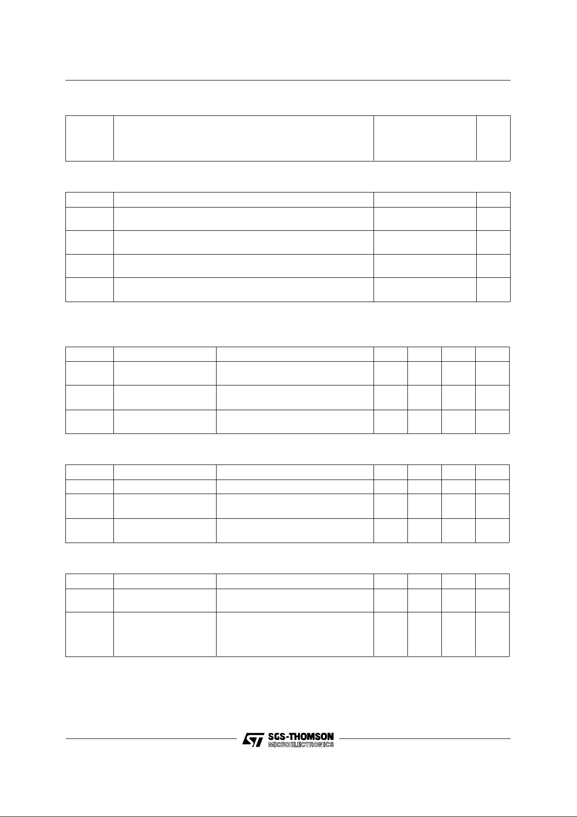
3
2
1
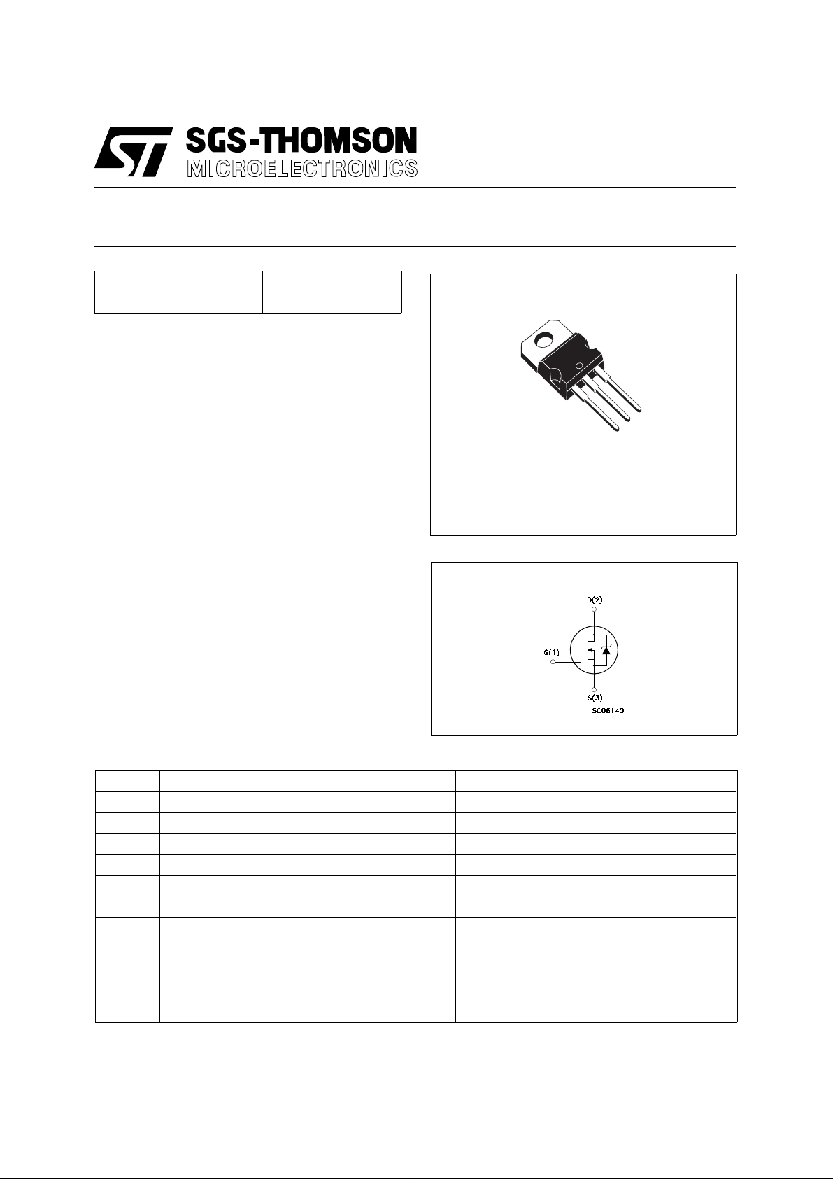
TO-220
INTERNAL SCHEMATIC DIAGRAM
ABSOL UT E MAXIMU M RATINGS
Symbol Parameter Value Unit
V
V
V
I
DM
P
dV/dt(
T
(•) Pulse width limited by safe operating area
March 1996
Drain-source Voltage (VGS = 0) 60 V
DS
Drain- gate Voltage (RGS = 20 kΩ)60V
DGR
Gate-source Voltage ± 20 V
GS
I
Drain Current (continuous) at Tc = 25 oC80A
D
I
Drain Current (continuous) at Tc = 100 oC60A
D
(•) Drain Current (pulsed) 320 A
Total Dissipation at Tc = 25 oC 150 W
tot
Derating Factor 1 W/
1) Peak Diode Recovery voltage slope 5 V/ns
Storage Temperature -65 to 175
stg
T
Max. Operating Junction Temperature 175
j
o
C
o
C
o
C
1/5
Page 2
STP80N06-10
THERMAL DATA
R
thj-case
R
thj-amb
R
thc-si n k
T
Thermal Resistance Junction-case Max
Thermal Resistance Junction-ambient Max
Thermal Resistance Case-sink Typ
Maximum Lead Temperature For Soldering Purpose
l
AVALANCHE CHARACTERI S TICS
Symbol Parameter Max Value Unit
I
AR
E
E
I
AR
Avalanche Current, Repetitive or Not-Repetitive
(pulse width limited by T
Single Pulse Avalanche Energy
AS
(starting T
Repetitive Avalanche Energy
AR
= 25 oC, ID = IAR, V
j
(pulse width limited by T
max, δ < 1%)
j
DD
max, δ < 1%)
j
Avalanche Current, Repetitive or Not-Repetitive
(T
= 100 oC, pulse width limited by Tj max, δ < 1%)
c
= 25 V)
1
62.5
0.5
300
60 A
600 mJ
150 mJ
60 A
o
C/W
o
C/W
o
C/W
o
C
ELECTRICAL CHARACTERISTICS (T
= 25 oC unless otherwise specified)
case
OFF
Symbol Parameter Test Conditions Min. Typ. Max. Unit
V
(BR)DSS
Drain-source
ID = 250 µA V
= 0 60 V
GS
Breakdown Voltage
I
DSS
I
GSS
Zero Gate Voltage
Drain Current (V
GS
Gate-body Leakage
Current (V
DS
= 0)
= 0)
= Max Rating
V
DS
V
= Max Rating x 0.8 Tc = 125 oC
DS
= ± 20 V ± 100 nA
V
GS
250
1000µAµA
ON (∗)
Symbol Parameter Test Conditions Min. Typ. Max. Unit
V
GS(th)
R
DS(on)
I
D(on)
Gate Threshold Voltage V
Static Drain-source On
Resistance
= VGS ID = 250 µA 234V
DS
VGS = 10V ID = 40 A
V
= 10V ID = 40 A Tc = 100oC
GS
On State Drain Current VDS > I
V
= 10 V
GS
D(on)
x R
DS(on)max
0.0085 0.01
0.02
80 A
DYNAMIC
Symbol Parameter Test Conditions Min. Typ. Max. Unit
g
(∗) Forward
fs
Transconductance
C
C
C
Input Capacitance
iss
Output Capacitance
oss
Reverse Transfer
rss
Capacitance
VDS > I
V
DS
x R
D(on)
DS(on)max
= 25 V f = 1 MHz V
ID = 40 A 25 S
= 0 5900
GS
900
230
Ω
Ω
pF
pF
pF
2/5
Page 3

STP80N06-10
ELECTRICAL CHARACTERISTICS (continued)
SWITCHING O N
Symbol Parameter Test Conditions Min. Typ. Max. Unit
t
d(on)
t
r
Turn-on Time
Rise Time
V
= 30 V ID = 40 A
DD
R
= 4.7 Ω VGS = 10 V
G
(see test circuit, figure 3)
(di/dt)
Turn-on Current Slope V
on
= 48 V ID = 80 A
DD
R
=50 Ω VGS = 10 V
G
(see test circuit, figure 5)
Q
Q
Q
Total Gate Charge
g
Gate-Source Charge
gs
Gate-Drain Charge
gd
V
= 40 V ID = 80 A V
DD
= 10 V 230
GS
SWITCHING O F F
Symbol Parameter Test Conditions Min. Typ. Max. Unit
t
r(Voff)
t
t
Off-voltage Rise Time
Fall Time
f
Cross-over Time
c
V
= 48 V ID = 40 A
DD
R
= 4.7 Ω VGS = 10 V
G
(see test circuit, figure 5)
SOURCE DRAIN DIO DE
32
16042200
240 A/µs
280 nC
30
60
35
175
240
46
230
300
ns
ns
nC
nC
ns
ns
ns
Symbol Parameter Test Conditions Min. Typ. Max. Unit
80
320
I
SDM
I
SD
Source-drain Current
(•)
Source-drain Current
(pulsed)
V
(∗) Forward On Voltage ISD = 80 A VGS = 0 1.5 V
SD
t
Reverse Recovery
rr
I
= 80 A di/dt = 100 A/µs
SD
125
Time
Q
I
RRM
Reverse Recovery
rr
Charge
Reverse Recovery
= 30 V Tj = 150 oC
V
R
(see test circuit, figure 5)
0.6
10
Current
(∗) Pulsed: Pulse duration = 300 µs, duty cycle 1.5 %
(•) Pulse width limited by safe operating area
1) I
≤ 60 A, di/dt ≤ 200 A/µs, VDD ≤ V
(
SD
(BR)DSS
, TJ ≤ T
JMAX
A
A
ns
µC
A
3/5
Page 4

E
STP80N06-10
TO-220 MECHANICAL DATA
DIM.
MIN. TYP. MAX. MIN. TYP. MAX.
A 4.40 4.60 0.173 0.181
C 1.23 1.32 0.048 0.051
D 2.40 2.72 0.094 0.107
D1 1.27 0.050
E 0.49 0.70 0.019 0.027
F 0.61 0.88 0.024 0.034
F1 1.14 1.70 0.044 0.067
F2 1.14 1.70 0.044 0.067
G 4.95 5.15 0.194 0.203
G1 2.4 2.7 0.094 0.106
H2 10.0 10.40 0.393 0.409
L2 16.4 0.645
L4 13.0 14.0 0.511 0.551
L5 2.65 2.95 0.104 0.116
L6 15.25 15.75 0.600 0.620
L7 6.2 6.6 0.244 0.260
L9 3.5 3.93 0.137 0.154
DIA. 3.75 3.85 0.147 0.151
mm inch
4/5
A
C
D
D1
L2
F1
L5
Dia.
G1
F
F2
L9
G
H2
L7
L6
L4
P011C
Page 5

STP80N06-10
Information furnished is believed to be accurate and reliable. However, SGS-THOMSON Microelectronics assumes no responsability for the
consequences of use of such information nor for any infringement of pat e nts or ot her rights o f third partie s which may results from its use. No
license is granted by implication or otherwise under any patent or patent rights of SG S-THOMSON Microelectroni cs. Specifications ment ioned
in this publication are subject to cha nge wi t hout n o tice. This p u bli ca t ion sup e rsed e s and r epla ces al l inf ormat i on pr ev io us ly supplied.
SGS-THOMSON Microelectronics products are not auth orized for use as critical components in life support devices or systems without express
written approval of SGS-THOM SO N M icroelecto nics.
© 1995 SGS-THOMSON Microelectronics - All Rights Reserved
Australia - Brazil - France - Germany - Hong Ko ng - Ita ly - Japa n - Korea - Mal ay sia - Mal ta - Mor oc co - The Net her l ands -
Singapore - Spain - Sweden - Switzerland - Taiwan - Thailand - United Kingdom - U.S.A
SGS-THOMSON Microelectronics GROUP OF COMPANIES
. . .
5/5
 Loading...