

Page 1
STP80N05-09
N - CHANNEL ENHANCEMENT MODE
”ULTRA HIGH DENSITY” POWER MOS TRANSISTOR
■ ULTRA HIGHDENSITY TECHNOLOGY
■ TYPICAL R
DS(on)
=7mΩ
■ AVALANCHE RUGGED TECHNOLOGY
■ LOW GATECHARGE
■ HIGH CURRENT CAPABILITY
■ 175
o
C OPERATING TEMPERATURE
APPLICATIONS
■ SYNCROUNOUS RECTIFIERS
■ HIGH CURRENT, HIGHSPEED SWITCHING
■ DC-DC &DC-AC CONVERTER ABSOLUTE
MAXIMUM RATINGS
INTERNAL SCHEMATIC DIAGRAM
March1997
ABSOLUTE MAXIMUM RATINGS
Symbol Parameter Value Unit
V
DS
Drain-source Voltage (VGS=0) 50 V
V
DGR
Drain- gate Voltage (RGS=20kΩ)50V
V
GS
Gate-source Voltage ± 20 V
I
D
Drain Current (continuous) at Tc=25oC80A
I
D
Drain Current (continuous) at Tc=100oC60A
I
DM
(•) Drain Current (pulsed) 320 A
P
tot
Total Dissipation at Tc=25oC 150 W
Derating Factor 1 W/oC
dV/dt(1) Peak Diode Recovery voltageslope 5 V/ns
T
stg
Storage Temperature -65 t o 175
o
C
T
j
Max. Operating Junction Temperature 175
o
C
(•) Pulse width limited bysafe operatingarea (1)ISD≤ 60 A,di/dt≤ 200 A/ms,VDD≤ V
(BR)DSS,TJ≤TJMAX
TYPE V
DSS
R
DS(on)
I
D
STP80N05-09 50 V < 0.009 Ω 80 A
1
2
3
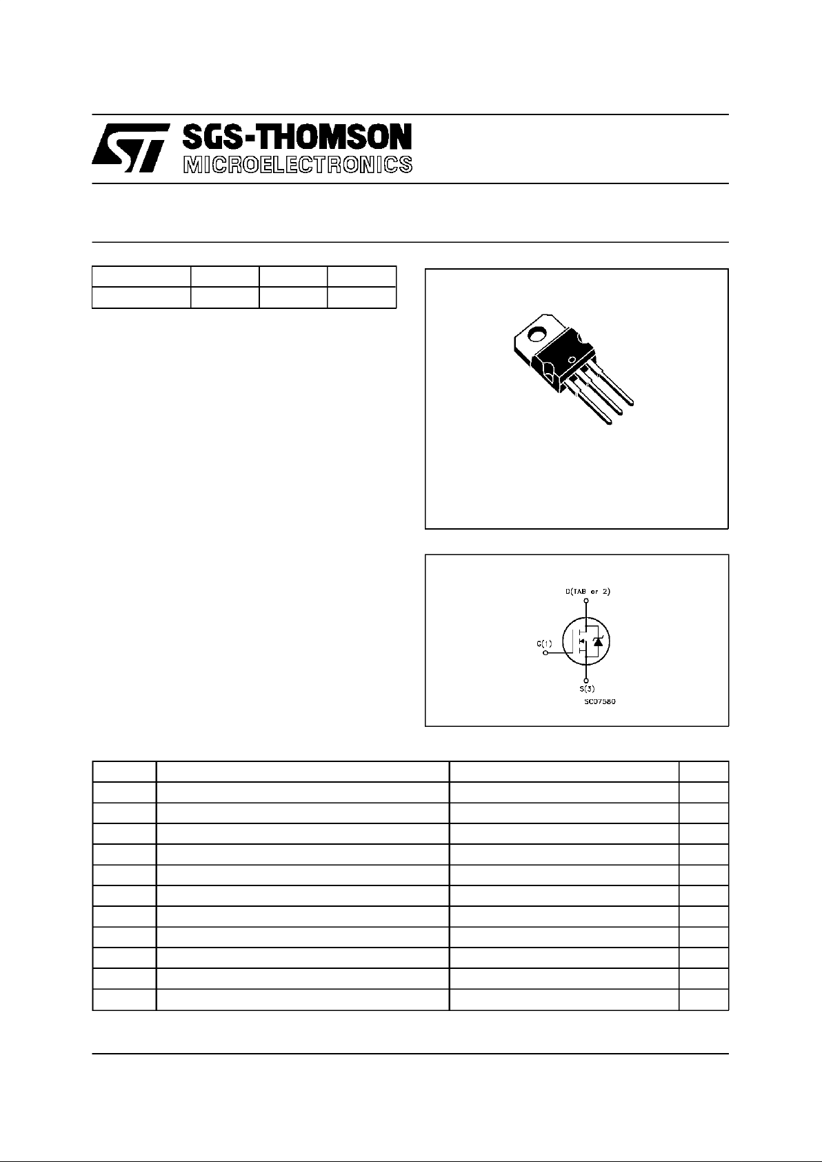
TO-220
1/9
Page 2
THERMAL DATA
R
thj-case
R
thj-amb
R
thc-sink
T
l
Thermal Resistance Junction-case Max
Thermal Resistance Junction-ambient Max
Thermal Resistance Case-sink Typ
Maximum Lead Temperature For Soldering Purpose
1
62.5
0.5
300
o
C/W
o
C/W
o
C/W
o
C
AVALANCHE CHARACTERISTICS
Symbol Parameter Max Value Unit
I
AR
Avalanche Current, Repetitive or Not-Repetitive
(pulse width limited by Tjmax,δ <1%)
60 A
E
AS
Single Pulse AvalancheEnergy
(starting Tj=25oC, ID=IAR,VDD=25V)
600 mJ
ELECTRICAL CHARACTERISTICS (T
case
=25oC unless otherwise specified)
OFF
Symbol Parameter Test Conditions Min. Typ. Max. Unit
V
(BR)DSS
Drain-source
Breakdown Voltage
ID=250µAVGS= 0 50 V
I
DSS
Zero Gate Voltage
Drain Current (VGS=0)
VDS=MaxRating
VDS= Max Rating Tc=125oC
1
10
µA
µA
I
GSS
Gate-body Leakage
Current (VDS=0)
VGS=± 20 V ± 100 nA
ON (∗)
Symbol Parameter Test Conditions Min. Typ. Max. Unit
V
GS(th)
Gate Threshold Voltage VDS=VGSID=250µA234V
R
DS(on)
Static Drain-source On
Resistance
VGS= 10V ID=40A 0.007 0.009 Ω
I
D(on)
On State Drain Current VDS>I
D(on)xRDS(on)max
VGS=10V
80 A
DYNAMIC
Symbol Parameter Test Conditions Min. Typ. Max. Unit
gfs(∗) Forward
Transconductance
VDS>I
D(on)xRDS(on)maxID
= 40 A 25 S
C
iss
C
oss
C
rss
Input Capacitance
Output Capacitance
Reverse Transfer
Capacitance
VDS=25V f=1MHz VGS=0 5900
900
230
pF
pF
pF
STP80N05-09
2/9
Page 3
ELECTRICAL CHARACTERISTICS (continued)
SWITCHING ON
Symbol Parameter Test Conditions Min. Typ. Max. Unit
t
d(on)
t
r
Turn-on Time
Rise T ime
VDD=30V ID=40A
RG=4.7 Ω VGS=10V
(see test circuit, figure 3)
32
16042200
ns
ns
(di/dt)onTurn-on Current Slop e VDD=48V ID=80A
RG=50 Ω VGS=10V
(see test circuit, figure 5)
240 A/µs
Q
g
Q
gs
Q
gd
Total Gate Charge
Gate-Source Charge
Gate-Drain Charge
VDD=40V ID=80A VGS= 10 V 230
30
60
280 nC
nC
nC
SWITCHING OFF
Symbol Parameter Test Conditions Min. Typ. Max. Unit
t
r(Voff)
t
f
t
c
Off-voltage Rise Time
Fall Ti me
Cross-over Time
VDD=48V ID=40A
RG=4.7 Ω VGS=10V
(see test circuit, figure 5)
35
175
240
46
230
300
ns
ns
ns
SOURCE DRAIN DIODE
Symbol Parameter Test Conditions Min. Typ. Max. Unit
I
SD
I
SDM
(•)
Source-drain Current
Source-drain Current
(pulsed)
80
320
A
A
VSD(∗) Forward On Voltage ISD=80A VGS=0 1.5 V
t
rr
Q
rr
I
RRM
ReverseRecovery
Time
ReverseRecovery
Charge
ReverseRecovery
Current
ISD= 80 A di/dt = 100 A/µs
VR=30V Tj=150oC
(see test circuit, figure 5)
125
0.6
10
ns
µC
A
(∗) Pulsed: Pulseduration =300 µs, duty cycle 1.5%
(•) Pulse widthlimitedby safe operatingarea
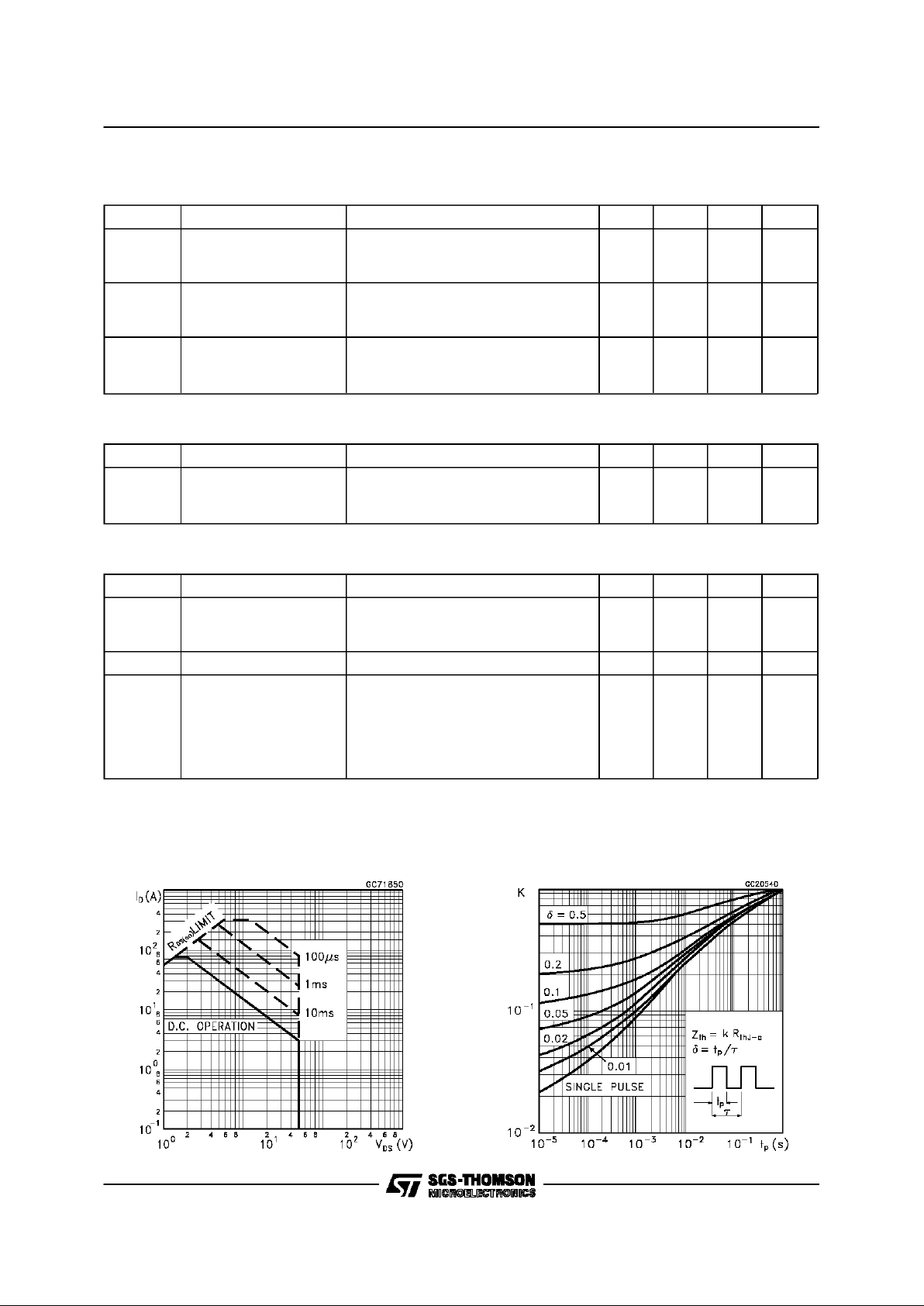
Safe Operating Area Thermal Impedance
STP80N05-09
3/9
Page 4

Derating Curve
Transfer Characteristics
Static Drain-source On Resistance
Output Characteristics
Transconductance
Gate Charge vs Gate-source Voltage
STP80N05-09
4/9
Page 5

Capacitance Variations
Normalized On Resistance vs Temperature
Turn-off Drain-source Voltage Slope
Normalized GateThreshold Voltage vs
Temperature
Turn-on Current Slope
Cross-over Time
STP80N05-09
5/9
Page 6

Switching Safe Operating Area
Source-drain Diode Forward Characteristics
Fig. 1: Unclamped Inductive Load TestCircuit
Accidental Overload Area
Fig. 2: Unclamped Inductive Waveform
STP80N05-09
6/9
Page 7

Fig. 3: Switching Times TestCircuits For
Resistive Load
Fig. 5: Test Circuit For Inductive Load Switching
And DIode RecoveryTimes
Fig. 4: Gate Charge test Circuit
STP80N05-09
7/9
Page 8

DIM.
mm inch
MIN. TYP. MAX. MIN. TYP. MAX.
A 4.40 4.60 0.173 0.181
C 1.23 1.32 0.048 0.051
D 2.40 2.72 0.094 0.107
D1 1.27 0.050
E 0.49 0.70 0.019 0.027
F 0.61 0.88 0.024 0.034
F1 1.14 1.70 0.044 0.067
F2 1.14 1.70 0.044 0.067
G 4.95 5.15 0.194 0.203
G1 2.4 2.7 0.094 0.106
H2 10.0 10.40 0.393 0.409
L2 16.4 0.645
L4 13.0 14.0 0.511 0.551
L5 2.65 2.95 0.104 0.116
L6 15.25 15.75 0.600 0.620
L7 6.2 6.6 0.244 0.260
L9 3.5 3.93 0.137 0.154
DIA. 3.75 3.85 0.147 0.151
L6
A
C
D
E
D1
F
G
L7
L2
Dia.
F1
L5
L4
H2
L9
F2
G1
TO-220 MECHANICAL DATA
P011C
STP80N05-09
8/9
Page 9

Information furnished is believed to be accurate and reliable. However, SGS-THOMSONMicroelectronics assumes no responsabilityfor the
consequences of use of such information nor for any infringement of patents or other rights of third parties which may results from its use. No
license is grantedby implication or otherwise under any patent or patentrights ofSGS-THOMSONMicroelectronics.Specifications mentioned
in this publication are subject to change without notice.This publicationsupersedes and replaces all informationpreviously supplied.
SGS-THOMSONMicroelectronics products arenot authorized for use as criticalcomponents in life support devices orsystems withoutexpress
written approval of SGS-THOMSONMicroelectonics.
1996 SGS-THOMSONMicroelectronics - Printed in Italy - All Rights Reserved
SGS-THOMSON MicroelectronicsGROUP OF COMPANIES
Australia - Brazil - Canada - China - France - Germany - Hong Kong - Italy- Japan - Korea - Malaysia - Malta - Morocco - TheNetherlands -
Singapore- Spain - Sweden- Switzerland- Taiwan - Thailand - United Kingdom - U.S.A
...
STP80N05-09
9/9
 Loading...