

Page 1

STP75NE75
STP75NE75FP
N - CHANNEL 75V - 0.01Ω - 75A TO-220/TO-220FP
STripFET POWER MOSFET
■ TYPICALR
DS(on)
= 0.01 Ω
■ EXCEPTIONALdv/dtCAPABILITY
■ 100%AVALANCHETESTED
■ APPLICATIONORIENTED
CHARACTERIZATION
DESCRIPTION
This Power MOSFET is the latestdevelopmentof
STMicroelectronics unique ”Single Feature
Size” strip-based process. The resultingtransi-
stor shows extremely high packingdensityfor low
on-resistance, rugged avalanche characteristics
and less critical alignment steps therefore a remarkablemanufacturingreproducibility.
APPLICATIONS
■ SOLENOIDAND RELAY DRIVERS
■ DC MOTOR CONTROL, AUDIO AMPLIFIERS
■ DC-DCCONVERTERS
■ AUTOMOTIVEENVIRONMENT
INTERNAL SCHEMATIC DIAGRAM
ABSOLUTE MAXIMUM RATINGS
Symbol Parameter Value Unit
ST P75NE75 S TP 75 NE 7 5F P
V
DS
Drain-source Voltage (VGS=0) 75 V
V
DGR
Drain- gate Vol t age (RGS=20kΩ)75V
V
GS
Gate-source Voltage ± 20 V
I
D
Drain Curre nt (cont i nuous) at Tc=25oC7540A
I
D
Drain Curre nt (cont i nuous) at Tc=100oC5328A
I
DM
(•) Dr ain Curre nt (pulse d) 300 160 A
P
tot
Total Dissipation at Tc=25oC 160 50 W
Derat ing F ac tor 1.06 0.37 W/
o
C
V
ISO
Ins ulat ion W i th s t and Voltage ( DC) 20 00 V
dv/ dt Pea k Diode Recovery voltage slope 7 V/ns
T
stg
Sto rage Temperat ure -65 to 175
o
C
T
j
Max. Operat ing Junct ion Tem pe ra ture 175
o
C
(•) Pulse width limited by safe operating area (1)ISD≤75 A, di/dt ≤ 300 A/µs, VDD≤ V
(BR)DSS,Tj≤TJMAX
TYPE V
DSS
R
DS(on)
I
D
ST P75NE75
ST P75NE75FP
75 V
75 V
<0.013Ω
<0.013Ω
75 A
40 A
May 1999
TO-220 TO-220FP
1
2
3
1
2
3
1/9
Page 2

THERMAL DATA
TO-220 TO-220FP
R
thj-case
Ther mal Resistanc e Junct ion-case Ma x 0.94 2.7
o
C/W
R
thj-amb
R
thc-sink
T
l
Ther mal Resistanc e Junct ion-ambient Max
Ther mal Resistanc e Case-sink Ty p
Maximum Lead Temperat ur e F or Soldering Purp ose
62.5
0.5
300
o
C/W
o
C/W
o
C
AVALANCHE CHARACTERISTICS
Symbol Parameter Max Valu e Unit
I
AR
Avalanche Current, R epetitive or Not-Repetitive
(pulse width limited by T
j
max)
75 A
E
AS
Single Pul se Avalanc he Ener gy
(starting T
j
=25oC, ID=IAR,VDD=30V)
200 mJ
ELECTRICAL CHARACTERISTICS
(T
case
=25oC unless otherwisespecified)
OFF
Symbol Parameter Test Conditions Min. Typ. Max. U nit
V
(BR)DSS
Drain-source
Break dow n Vo lt age
ID=250µAVGS=0 75 V
I
DSS
Zero Gate Voltage
Drain Curre nt (V
GS
=0)
V
DS
=MaxRating
V
DS
=MaxRating Tc= 125oC
1
10
µA
µA
I
GSS
Gat e- bod y Leakag e
Current (V
DS
=0)
V
GS
=± 20 V
±
100 nA
ON (∗)
Symbol Parameter Test Conditions Min. Typ. Max. U nit
V
GS(th)
Gate Threshold Voltage VDS=VGSID= 250µA 234V
R
DS(on)
Sta t ic Drain-s our c e On
Resistance
VGS=10V ID= 37.5 A 0.01 0.01 3
Ω
I
D(on)
On State Drain Current VDS>I
D(on)xRDS(on)max
VGS=10V
75 A
DYNAMIC
Symbol Parameter Test Conditions Min. Typ. Max. U nit
g
fs
(∗)Forward
Tr ansc on duc tance
VDS>I
D(on)xRDS(on)maxID
=37. 5 A 40 S
C
iss
C
oss
C
rss
Input Capaci t ance
Out put Capac itance
Reverse Transfer
Capacit a nc e
VDS=25V f=1MHz VGS= 0 5300
850
310
pF
pF
pF
STP75NE75/FP
2/9
Page 3
ELECTRICAL CHARACTERISTICS
(continued)
SWITCHINGON
Symbol Parameter Test Conditions Min. Typ. Max. U nit
t
d(on)
t
r
Tur n-on Delay Time
Rise Time
VDD=40V ID=40A
R
G
=4.7
Ω
VGS=10V
(Resis t iv e Load, see fig. 3 )
32
130
ns
ns
Q
g
Q
gs
Q
gd
Tot al Gate Charge
Gat e- Source Charge
Gate-Drain Charge
VDD=60V ID=75A VGS= 10 V 150
30
62
200 nC
nC
nC
SWITCHINGOFF
Symbol Parameter Test Conditions Min. Typ. Max. U nit
t
d(off)
t
f
Tur n-of f Dela y Tim e
Fall T ime
VDD=40V ID=40A
R
G
=4.7 Ω VGS=10V
(Resis t iv e Load, see fig. 3 )
150
45
ns
ns
t
r(Voff)
t
f
t
c
Off-voltage Rise T im e
Fall T ime
Cross-over Tim e
V
clamp
=60V ID=75A
R
G
=4.7 Ω VGS=4.5V
(Indu ct iv e Load, see fig. 5)
35
60
100
ns
ns
ns
SOURCEDRAINDIODE
Symbol Parameter Test Conditions Min. Typ. Max. U nit
I
SD
I
SDM
(•)
Source-drain Current
Source-drain Current
(pulsed)
43
170
A
A
V
SD
(∗)ForwardOnVoltage ISD=75A VGS=0 1.5 V
t
rr
Q
rr
I
RRM
Reverse Recovery
Time
Reverse Recovery
Charge
Reverse Recovery
Current
ISD= 75 A di/dt = 100 A /µs
V
DD
=30V Tj=150oC
(see test circuit, fig. 5)
130
0.6
9
ns
µC
A
(∗) Pulsed: Pulse duration = 300 µs, duty cycle 1.5 %
(•) Pulse width limited by safe operating area
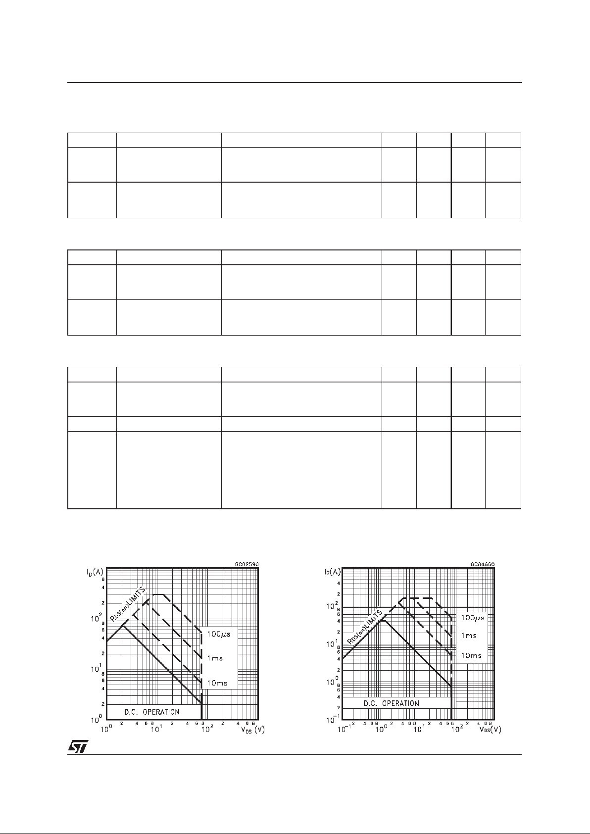
SafeOperating Area for TO-220 SafeOperating Area for TO-220FP
STP75NE75/FP
3/9
Page 4

ThermalImpedancefor TO-220
OutputCharacteristics
Transconductance
ThermalImpedanceforTO-220FP
TransferCharacteristics
Static Drain-sourceOn Resistance
STP75NE75/FP
4/9
Page 5

Gate Charge vs Gate-sourceVoltage
NormalizedGate ThresholdVoltage vs
Temperature
Source-drainDiode Forward Characteristics
CapacitanceVariations
NormalizedOn Resistancevs Temperature
STP75NE75/FP
5/9
Page 6

Fig. 1: Unclamped InductiveLoad Test Circuit
Fig. 3: Switching Times Test Circuits For
ResistiveLoad
Fig. 2: Unclamped InductiveWaveform
Fig. 4: Gate Chargetest Circuit
Fig. 5: Test Circuit For Inductive Load Switching
And Diode Recovery Times
STP75NE75/FP
6/9
Page 7

DIM.
mm inch
MIN. TYP. MAX. MIN. TYP. MAX.
A 4.40 4.60 0.173 0.181
C 1.23 1.32 0.048 0.051
D 2.40 2.72 0.094 0.107
D1 1.27 0.050
E 0.49 0.70 0.019 0.027
F 0.61 0.88 0.024 0.034
F1 1.14 1.70 0.044 0.067
F2 1.14 1.70 0.044 0.067
G 4.95 5.15 0.194 0.203
G1 2.4 2.7 0.094 0.106
H2 10.0 10.40 0.393 0.409
L2 16.4 0.645
L4 13.0 14.0 0.511 0.551
L5 2.65 2.95 0.104 0.116
L6 15.25 15.75 0.600 0.620
L7 6.2 6.6 0.244 0.260
L9 3.5 3.93 0.137 0.154
DIA. 3.75 3.85 0.147 0.151
L6
A
C
D
E
D1
F
G
L7
L2
Dia.
F1
L5
L4
H2
L9
F2
G1
TO-220 MECHANICAL DATA
P011C
STP75NE75/FP
7/9
Page 8

DIM.
mm inch
MIN. TYP. MAX. MIN. TYP. MAX.
A 4.4 4.6 0.173 0.181
B 2.5 2.7 0.098 0.106
D 2.5 2.75 0.098 0.108
E 0.45 0.7 0.017 0.027
F 0.75 1 0.030 0.039
F1 1.15 1.7 0.045 0.067
F2 1.15 1.7 0.045 0.067
G 4.95 5.2 0.195 0.204
G1 2.4 2.7 0.094 0.106
H 10 10.4 0.393 0.409
L2 16 0.630
L3 28.6 30.6 1.126 1.204
L4 9.8 10.6 0.385 0.417
L6 15.9 16.4 0.626 0.645
L7 9 9.3 0.354 0.366
Ø 3 3.2 0.118 0.126
L2
A
B
D
E
H
G
L6
¯
F
L3
G1
123
F2
F1
L7
L4
TO-220FP MECHANICAL DATA
STP75NE75/FP
8/9
Page 9

Information furnishedis believedto beaccurate and reliable.However, STMicroelectronics assumes no responsibilityfor the consequences
of use of such information nor for any infringement of patents or other rights of third parties which may result from its use. No license is
granted by implication or otherwise under any patent or patent rights of STMicroelectronics. Specification mentioned in this publicationare
subjectto change without notice. This publication supersedes andreplaces all information previouslysupplied. STMicroelectronicsproducts
are not authorized for useas critical components in lifesupport devicesor systemswithout express written approval of STMicroelectronics.
The ST logo is a trademark of STMicroelectronics
1999 STMicroelectronics – Printed in Italy – All Rights Reserved
STMicroelectronics GROUP OF COMPANIES
Australia - Brazil - Canada - China - France - Germany - Italy - Japan - Korea - Malaysia - Malta - Mexico - Morocco - The Netherlands -
Singapore - Spain - Sweden - Switzerland - Taiwan - Thailand - United Kingdom - U.S.A.
http://www.st.com
.
STP75NE75/FP
9/9
 Loading...