

Page 1
STP6NC60
N - CHANNEL 600V - 1.0 Ω - 6A TO-220/TO-220FP
TYPE V
STP6NC60
STP6NC60FP
■ TYPICALR
■ EXTREMELYHIGH dv/dt CAPABILITY
■ 100%AVALANCHETESTED
■ NEWHIGH VOLTAGE BENCHMARK
■ GATECHARGE MINIMIZED
DS(on)
DSS
600 V
600 V
= 1.0 Ω
DESCRIPTION
The PowerMESHΙΙ is the evolution of the first
generation of MESH OVERLAY. The layout
refinements introduced greatly improve the
Ron*areafigure of merit while keeping the device
at the leading edge for what concerns switching
speed,gate chargeand ruggedness.
APPLICATIONS
■ HIGHCURRENT, HIGH SPEED SWITCHING
■ SWITHMODE POWER SUPPLIES(SMPS)
■ DC-AC CONVERTERS FOR WELDING
EQUIPMENTANDUNINTERRUPTIBLE
POWERSUPPLIESAND MOTOR DRIVER
R
DS(on)
<1.2
<1.2 Ω
I
D
Ω
6A
6A
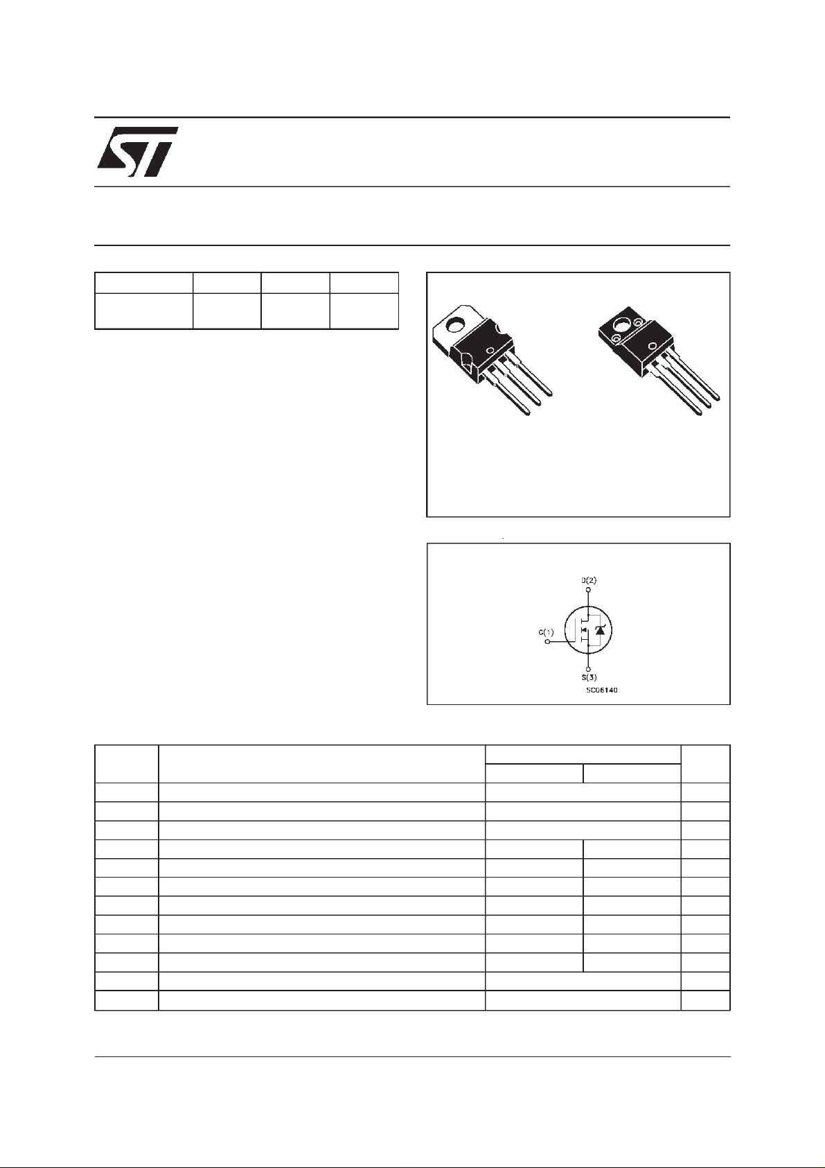
STP6NC60FP
PowerMESHΙΙ MOSFET
3
2
1
TO-220 T0-220FP
INTERNAL SCHEMATIC DIAGRAM
3
2
1
ABSOLUTE MAXIMUM RATINGS
Symbol Parameter Value Unit
ST P6NC6 0 ST P6NC 60FP
V
V
V
I
DM
P
dv/dt(
V
T
(•) Pulse width limited by safe operating area (1)ISD≤ 6 A,di/dt ≤100 A/µs,VDD≤ V
(*) Limited only by maximum temperatureallowed
December 1999
Drain-source Volt age (VGS= 0) 600 V
DS
Drain- g at e V olt ag e (RGS=20kΩ) 600 V
DGR
Gate-s ource Voltage ± 30 V
GS
Drain Cur rent (co nt inu ous ) at Tc=25oC 6 6(*) A
I
D
Drain Cur rent (co nt inu ous ) at Tc=100oC 3.8 3.8(* ) A
I
D
(•) Drain Cur rent (puls ed) 24 24 A
Tot al Dissi pat ion at Tc=25oC 125 40 W
tot
Derat ing F ac tor 1.0 0. 32 W/
) P eak Diode Recov e ry voltage sl ope 4 4 V/ns
1
Ins ulat i on Wi t hs t an d V olt ag e (DC)
ISO
Sto rage Temper at ure -65 to 150
stg
Max. Operating Junc t ion Temperat ur e 150
T
j
2000 V
,Tj≤T
(BR)DSS
JMAX
o
C
o
C
o
C
1/9
Page 2
STP6NC60/STP6NC60FP
THERMAL DATA
T0-220 T0-220FP
R
thj-case
Rthj-amb
R
thc-sink
T
AVALANCHE CHARACTERISTICS
Symbol Parameter Max Valu e Unit
I
AR
E
Ther mal Res istance Junct ion-case Max 1.0 3.1
MaxT hermal Re sistance J unction-ambient Max
Ther mal Res istance C as e - sink Ty p
Maximum Lead Tempera t ure For Soldering Purpose
l
Avalanche Current, Repetitive or Not-Repetitive
(pulse width limited by T
Single Pul se A v alan c he E nergy
AS
(starting T
=25oC, ID=IAR,VDD=50V)
j
max)
j
62.5
0.5
300
6A
320 mJ
o
C/W
o
C/W
o
C/W
o
C
ELECTRICAL CHARACTERISTICS
=25oC unless otherwisespecified)
(T
case
OFF
Symbol Parameter Test Condit ions Min. Typ. Max. Unit
V
(BR)DSS
Drain-source
ID=250µAVGS= 0 600 V
Break dow n Vo lt age
I
DSS
I
GSS
Zero Gate Voltage
Drain Curre nt (V
GS
Gat e- bod y Leakag e
Current (V
DS
=0)
=0)
V
=MaxRating
DS
=MaxRating Tc=125oC
V
DS
= ± 30 V ± 100 nA
V
GS
1
50
ON(∗)
Symbol Parameter Test Condit ions Min. Typ. Max. Unit
V
GS(th)
R
DS(on)
Gate Threshold Voltage VDS=VGSID= 250 µA 234V
Sta t ic Drain-s our c e On
VGS=10V ID=3A 1.0 1.2 Ω
Resistance
I
D(on)
On State Drain Current VDS>I
D(on)xRDS(on)ma x
6A
VGS=10V
DYNAMIC
Symbol Parameter Test Condit ions Min. Typ. Max. Unit
g
(∗)Forward
fs
Tr ansc on duc tance
C
C
C
Input Capacit anc e
iss
Out put Capac itance
oss
Reverse Transfer
rss
Capacit a nc e
VDS>I
D(on)xRDS(on)ma xID
=3A 6.5 S
VDS=25V f=1MHz VGS= 0 1020
145
21
µA
µA
pF
pF
pF
2/9
Page 3
STP6NC60/STP6NC60FP
ELECTRICAL CHARACTERISTICS
(continued)
SWITCHINGON
Symbol Parameter Test Condit ions Min. Typ. Max. Unit
t
d(on)
t
r
Turn-on Time
Rise T ime
VDD=300V ID=3A
R
=4.7
G
Ω
VGS=10V
16
14
(see test circuit, figure 3)
Q
Q
Q
Tot al Gate Char ge
g
Gat e- Source Charge
gs
Gate-Drain Charge
gd
VDD= 480 V ID=6A VGS=10V 35
5.5
17.2
45.5 nC
SWITCHINGOFF
Symbol Parameter Test Condit ions Min. Typ. Max. Unit
t
r(Voff)
t
t
Off-voltage Ris e Time
Fall T ime
f
Cross-over Time
c
VDD=480V ID=6A
=4.7 Ω VGS=10V
R
G
(see test circuit, figure 5)
13
16
23
SOURCEDRAINDIODE
Symbol Parameter Test Condit ions Min. Typ. Max. Unit
I
SD
I
SDM
V
SD
t
Q
I
RRM
(∗) Pulsed:Pulse duration = 300µs, duty cycle 1.5%
(•) Pulse width limited by safeoperating area
Source-drain Current
(•)
Source-drain Current
6
24
(pulsed)
(∗)ForwardOnVoltage ISD=6A VGS=0 1.6 V
Reverse Recovery
rr
Time
Reverse Recovery
rr
ISD=6A di/dt=100A/µs
= 100 V Tj=150oC
V
DD
(see test circuit, figure 5)
450
2.9
Charge
Reverse Recovery
13
Current
ns
ns
nC
nC
ns
ns
ns
A
A
ns
µ
A
C
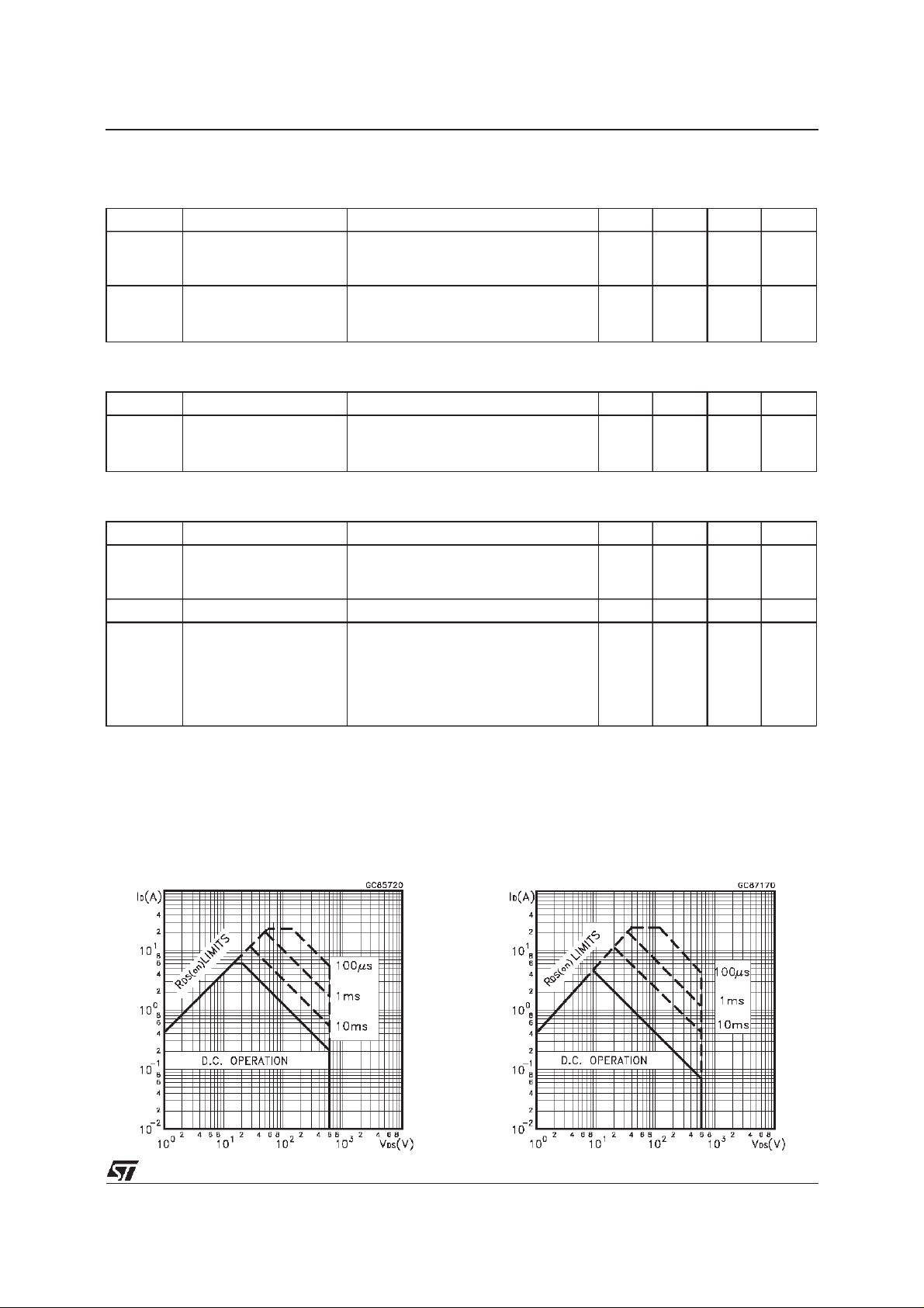
SafeOperating Area SafeOperating Area for TO-220FP
3/9
Page 4

STP6NC60/STP6NC60FP
ThermalImpedence
OutputCharacteristics
ThermalImpedencefor TO-220FP
TranferCharacteristics
Transconductance
4/9
Static Drain-sourceOn Resistance
Page 5

STP6NC60/STP6NC60FP
Gate Charge vs Gate-sourceVoltage
NormalizedGate ThresholdVoltage vs
Temperature
CapacitanceVariation
NormalizedOn Resistancevs Temperature
Source-drainDiode Forward Characteristics
5/9
Page 6

STP6NC60/STP6NC60FP
Fig. 1:
UnclampedInductiveLoad Test Circuit
Fig. 3: SwitchingTimes Test CircuitsFor
ResistiveLoad
Fig. 2:
UnclampedInductive Waveform
Fig. 4: Gate Charge test Circuit
Fig. 5:
Test CircuitFor InductiveLoad Switching
And Diode Recovery Times
6/9
Page 7

TO-220 MECHANICALDATA
STP6NC60/STP6NC60FP
DIM.
MIN. TYP. MAX. MIN. TYP. MAX.
A 4.40 4.60 0.173 0.181
C 1.23 1.32 0.048 0.051
D 2.40 2.72 0.094 0.107
D1 1.27 0.050
E 0.49 0.70 0.019 0.027
F 0.61 0.88 0.024 0.034
F1 1.14 1.70 0.044 0.067
F2 1.14 1.70 0.044 0.067
G 4.95 5.15 0.194 0.203
G1 2.4 2.7 0.094 0.106
H2 10.0 10.40 0.393 0.409
L2 16.4 0.645
L4 13.0 14.0 0.511 0.551
L5 2.65 2.95 0.104 0.116
L6 15.25 15.75 0.600 0.620
L7 6.2 6.6 0.244 0.260
L9 3.5 3.93 0.137 0.154
DIA. 3.75 3.85 0.147 0.151
mm inch
E
A
L4
D
F2
F1
G1
H2
G
F
P011C
C
D1
L2
Dia.
L5
L7
L6
L9
7/9
Page 8

STP6NC60/STP6NC60FP
TO-220FPMECHANICAL DATA
DIM.
MIN. TYP. MAX. MIN. TYP. MAX.
A 4.4 4.6 0.173 0.181
B 2.5 2.7 0.098 0.106
D 2.5 2.75 0.098 0.108
E 0.45 0.7 0.017 0.027
F 0.75 1 0.030 0.039
F1 1.15 1.7 0.045 0.067
F2 1.15 1.7 0.045 0.067
G 4.95 5.2 0.195 0.204
G1 2.4 2.7 0.094 0.106
H 10 10.4 0.393 0.409
L2 16 0.630
L3 28.6 30.6 1.126 1.204
L4 9.8 10.6 0.385 0.417
L6 15.9 16.4 0.626 0.645
L7 9 9.3 0.354 0.366
Ø 3 3.2 0.118 0.126
mm inch
E
A
D
8/9
B
L3
L6
L7
¯
F1
F
G1
H
F2
123
L2
L4
G
Page 9

STP6NC60/STP6NC60FP
Information furnished is believed tobe accurateand reliable.However, STMicroelectronics assumesnoresponsibilityforthe consequences
of use of such information nor for any infringement of patents or other rights of third parties which may result from its use. No license is
granted by implication or otherwise under any patent or patent rights of STMicroelectronics. Specificationmentioned in thispublication are
subjecttochange without notice.This publication supersedes and replacesall information previously supplied. STMicroelectronics products
are not authorized for use as critical components in life support devices or systemswithout express written approval of STMicroelectronics.
The STlogo is a trademark ofSTMicroelectronics
1999STMicroelectronics – Printedin Italy – All Rights Reserved
STMicroelectronics GROUP OF COMPANIES
Australia - Brazil - China- Finland - France - Germany - Hong Kong - India - Italy - Japan - Malaysia - Malta - Morocco -
Singapore - Spain - Sweden - Switzerland - United Kingdom- U.S.A.
http://www.st.com
.
9/9
 Loading...