

Page 1
STP6NB80
STP6NB80FP
N - CHANNEL 800V - 1.6
TYPE V
STP6NB80
STP6NB80FP
■ TYPICALR
■ EXTREMELYHIGH dv/dt CAPABILITY
■ 100%AVALANCHETESTED
■ VERYLOW INTRINSIC CAPACITANCES
■ GATECHARGEMINIMIZED
DS(on)
DSS
800 V
800 V
= 1.6 Ω
DESCRIPTION
Using the latest high voltageMESH OVERLAY
process, STMicroelectronics has designed an
advanced family of power MOSFETs with
outstanding performances. The new patent
pending strip layout coupled with the Company’s
proprietary edge termination structure, gives the
lowest RDS(on) per area, exceptional avalanche
and dv/dt capabilities and unrivalled gate charge
and switchingcharacteristics.
R
DS(on)
<1.9
Ω
<1.9Ω
I
D
5.7 A
5.7 A
Ω
- 5.7A- TO-220/TO-220FP
PowerMESH MOSFET
PRELIMINARY DATA
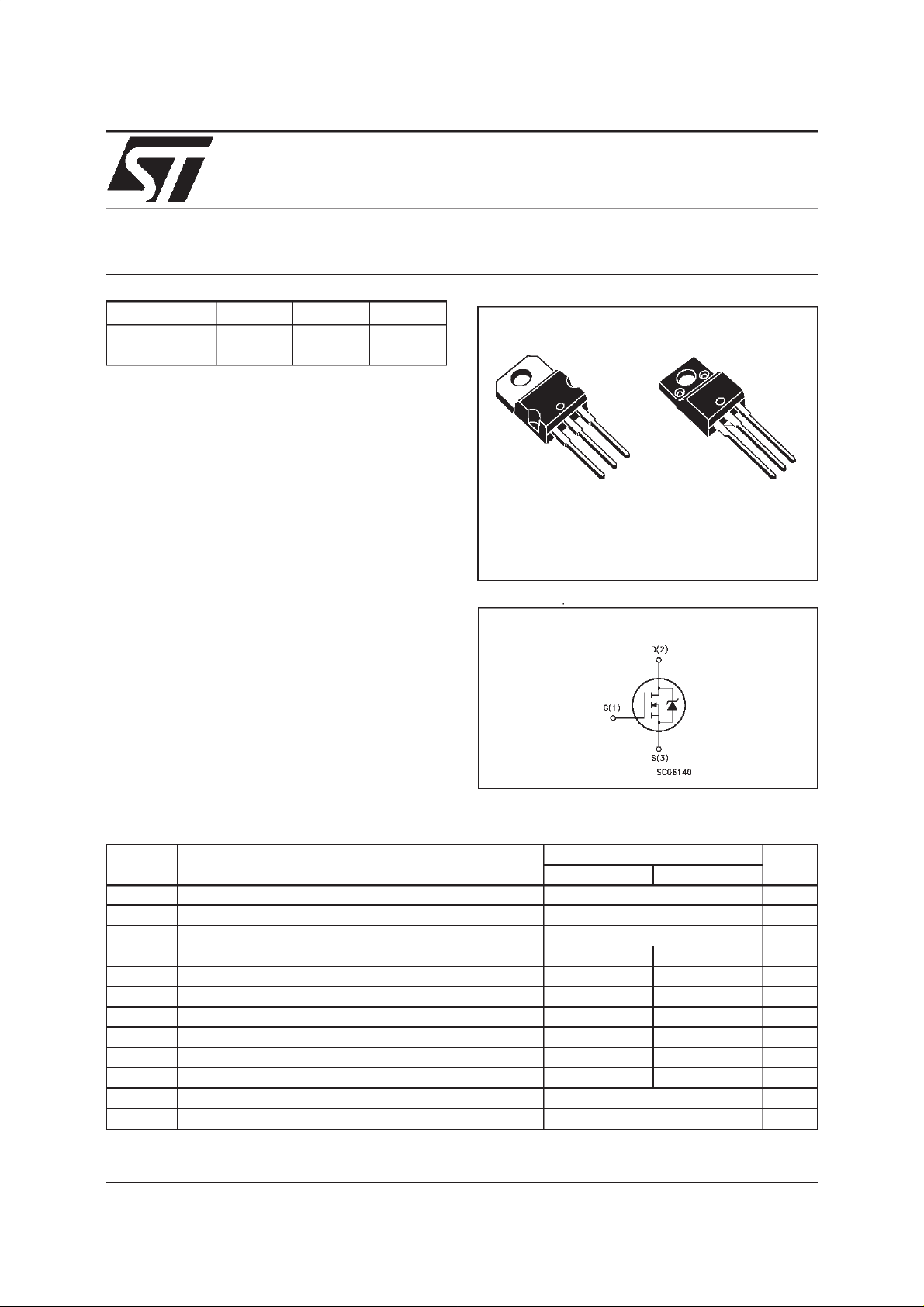
3
2
1
TO-220 TO-220FP
INTERNAL SCHEMATIC DIAGRAM
3
2
1
APPLICATIONS
■ HIGHCURRENT, HIGH SPEED SWITCHING
■ SWITCHMODEPOWER SUPPLIES(SMPS)
■ DC-ACCONVERTERSFOR WELDING
EQUIPMENTANDUNINTERRUPTIBLE
POWERSUPPLIESAND MOTOR DRIVE
ABSOLUTE MAXIMUM RATINGS
Symbol Parameter Value Unit
ST P6NB8 0 ST P6NB 80FP
V
V
V
I
DM
P
dv/dt(
V
T
(•) Pulse width limitedby safe operating area (1)I
*) Limited only maximum temperature allowed
(
September 1998
Drain-source Voltage (VGS= 0) 800 V
DS
Dra in- gat e Voltag e (RGS=20kΩ)
DGR
Gat e-source Voltage ± 30 V
GS
Dra in Cur re nt (cont inuous) at Tc=25oC 5.7 5.7(* ) A
I
D
Dra in Cur re nt (cont inuous) at Tc= 100oC3.62A
I
D
800 V
(•) Dra in Cur re nt (pulsed) 22.8 22.8 A
Tot al Dis sipati on at Tc=25oC 125 40 W
tot
Der ati ng Fact or 1.0 0.32 W/
1) Peak Diode Recove ry volt age slop e 4 4 V/ns
Insulation Withstand Voltage (DC)
ISO
St orage Temper at ure -65 to 150
stg
Max. Operating Junc t io n Tem p erat ure 150
T
j
≤
5.76 A, di/dt≤200 A/µs, V
SD
2000 V
≤
V
DD
(BR)DSS
,Tj≤T
JMAX
o
C
o
C
o
C
1/6
Page 2

STP6NB80/FP
THERMAL DATA
TO-220 TO220-FP
R
thj-case
R
thj-amb
R
thc-sink
T
AVALANCHE CHARACTERISTICS
Symbol Parameter Max Valu e Unit
I
AR
E
Thermal Resistance Junction-case Max 1.0 3.1
Thermal Resistance Junction-ambient Max
Thermal Resistance Case-sink Typ
Maximum Lead Temper at ure For Sold er ing Pu rpos e
l
Avalanc h e Current , Repet it i ve or Not-Repe t itive
(pulse w idth l imited by T
Single P ulse A valanche Energy
AS
(starting T
=25oC, ID=IAR,VDD=50V)
j
max)
j
62.5
0.5
300
5.7 A
314 mJ
o
C/W
o
C/W
o
C/W
o
C
ELECTRICAL CHARACTERISTICS
=25oC unless otherwise specified)
(T
case
OFF
Symbol Parameter Test Conditions M in. Typ. Max. Unit
V
(BR)DSS
Drain-source
=250µAVGS=0
I
D
800 V
Break dow n Vo lt a ge
I
DSS
I
GSS
Zero Gate Voltage
Drain Current (V
GS
Gat e- bod y Leakag e
Current (V
DS
=0)
=0)
V
=MaxRating
DS
=MaxRating Tc= 125oC
V
DS
= ± 30 V
V
GS
1
50
100 nA
±
ON(∗)
Symbol Parameter Test Conditions M in. Typ. Max. Unit
V
GS(th)
R
DS(on)
Gat e Thresho ld Vol t age
Static Drain-source On
V
DS=VGSID
= 250µA
VGS=10V ID=3A 1.6 1.9 Ω
345V
Resistance
I
D(on)
On S tate Drain Current VDS>I
D(on)xRDS(on)max
5.7 A
VGS=10V
DYNAMIC
Symbol Parameter Test Conditions M in. Typ. Max. Unit
gfs(∗)Forward
Tr ansc on duc tance
C
C
C
Input Capaci t an ce
iss
Out put Capac itance
oss
Reverse Transfer
rss
Capacit a nc e
VDS>I
D(on)xRDS(on)maxID
=3A 2.5 4.5 S
VDS=25V f=1MHz VGS= 0 1250
145
16
1625
190
21
µA
µA
pF
pF
pF
2/6
Page 3

STP6NB80/FP
ELECTRICAL CHARACTERISTICS
(continued)
SWITCHINGON
Symbol Parameter Test Conditions M in. Typ. Max. Unit
t
d(on)
Q
Q
Q
Turn-on Time
t
Rise Tim e
r
Total Gate Charge
g
Gat e- Source Charge
gs
Gate-Drain Charge
gd
VDD=400V ID=3A
=4.7 Ω VGS=10V
R
G
VDD= 640 V ID=6A VGS=10V 33
19
9
11
14
27
13
47 nC
SWITCHINGOFF
Symbol Parameter Test Conditions M in. Typ. Max. Unit
t
r(Voff)
t
t
Off -voltage Ri se Time
Fall Time
f
Cross-over Time
c
VDD= 640V ID=6A
=4.7 ΩVGS=10V
R
G
11
9
16
16
13
23
SOURCEDRAINDIODE
Symbol Parameter Test Conditions M in. Typ. Max. Unit
I
V
I
SDM
SD
Q
I
RRM
SD
t
Source-drain Current
(•)
Source-drain Current
5.7
22.8
(pulsed)
(∗) For ward On Voltage ISD=6A VGS=0 1.6 V
Reverse Recovery
rr
Time
Reverse Recovery
rr
= 6 A di/ dt = 100 A/µs
I
SD
= 100 V Tj=150oC
V
DD
700
5.8
Charge
Reverse Recovery
16.5
Current
ns
ns
nC
nC
ns
ns
ns
A
A
ns
µC
A
(∗) Pulsed:Pulse duration= 300 µs, duty cycle 1.5 %
(•) Pulse width limited by safe operatingarea
3/6
Page 4

STP6NB80/FP
TO-220 MECHANICAL DATA
DIM.
MIN. TYP. MAX. MIN. TYP. MAX.
A 4.40 4.60 0.173 0.181
C 1.23 1.32 0.048 0.051
D 2.40 2.72 0.094 0.107
D1 1.27 0.050
E 0.49 0.70 0.019 0.027
F 0.61 0.88 0.024 0.034
F1 1.14 1.70 0.044 0.067
F2 1.14 1.70 0.044 0.067
G 4.95 5.15 0.194 0.203
G1 2.4 2.7 0.094 0.106
H2 10.0 10.40 0.393 0.409
L2 16.4 0.645
L4 13.0 14.0 0.511 0.551
L5 2.65 2.95 0.104 0.116
L6 15.25 15.75 0.600 0.620
L7 6.2 6.6 0.244 0.260
L9 3.5 3.93 0.137 0.154
DIA. 3.75 3.85 0.147 0.151
mm inch
E
A
L4
D
F2
F1
G1
H2
G
F
P011C
C
D1
L2
Dia.
L5
L7
L6
L9
4/6
Page 5

TO-220FP MECHANICAL DATA
STP6NB80/FP
DIM.
MIN. TYP. MAX. MIN. TYP. MAX.
A 4.4 4.6 0.173 0.181
B 2.5 2.7 0.098 0.106
D 2.5 2.75 0.098 0.108
E 0.45 0.7 0.017 0.027
F 0.75 1 0.030 0.039
F1 1.15 1.7 0.045 0.067
F2 1.15 1.7 0.045 0.067
G 4.95 5.2 0.195 0.204
G1 2.4 2.7 0.094 0.106
H 10 10.4 0.393 0.409
L2 16 0.630
L3 28.6 30.6 1.126 1.204
L4 9.8 10.6 0.385 0.417
L6 15.9 16.4 0.626 0.645
L7 9 9.3 0.354 0.366
Ø 3 3.2 0.118 0.126
mm inch
E
A
D
B
L3
L6
L7
¯
F1
F
G1
H
G
F2
123
L2
L4
5/6
Page 6

STP6NB80/FP
Information furnished is believed to be accurate and reliable. However, STMicroelectronics assumes no responsibility for the consequences
of use of such information nor for any infringement of patents or other rights of third parties which may result from its use. No license is
granted by implication or otherwise under any patent or patent rights of STMicroelectronics. Specification mentioned in this publication are
subject to change without notice. This publication supersedes and replaces all information previously supplied. STMicroelectronics products
are not authorized for use as critical components in life support devices orsystems without express written approval ofSTMicroelectronics.
The ST logo is a trademarkof STMicroelectronics
1998 STMicroelectronics – Printed in Italy – All Rights Reserved
STMicroelectronics GROUP OF COMPANIES
Australia - Brazil - Canada -China - France -Germany - Italy - Japan - Korea - Malaysia - Malta - Mexico - Morocco - The Netherlands -
Singapore - Spain - Sweden - Switzerland - Taiwan - Thailand - United Kingdom - U.S.A.
http://www.st.com
.
6/6
 Loading...