

Page 1
STP6NB50
STP6NB50FP
N - CHANNEL ENHANCEMENT MODE
PowerMESH MOSFET
TYPE V
STP6NB50
STP6NB50FP
■ TYPICALR
■ EXTREMELY HIGH dv/dt CAPABILITY
■ 100% AVALANCHETESTED
■ VERYLOW INTRINSICCAPACITANCES
■ GATECHARGEMINIMIZED
DS(on)
DSS
500 V
500 V
=1.35 Ω
R
DS(on)
<1.5Ω
<1.5Ω
I
D
5.8 A
3.4 A
DESCRIPTION
Using the latest high voltageMESH OVERLAY
process, SGS-Thomson has designed an
advanced family of power MOSFETs with
outstanding performances. The new patent
pending strip layout coupled with the Company’s
proprietary edge termination structure, gives the
lowest RDS(on) per area, exceptional avalanche
and dv/dt capabilities and unrivalled gate charge
and switchingcharacteristics.
APPLICATIONS
■ HIGH CURRENT, HIGH SPEED SWITCHING
■ SWITCHMODEPOWER SUPPLIES(SMPS)
■ DC-ACCONVERTERS FOR WELDING
EQUIPMENTAND UNINTERRUPTIBLE
POWERSUPPLIESAND MOTORDRIVE
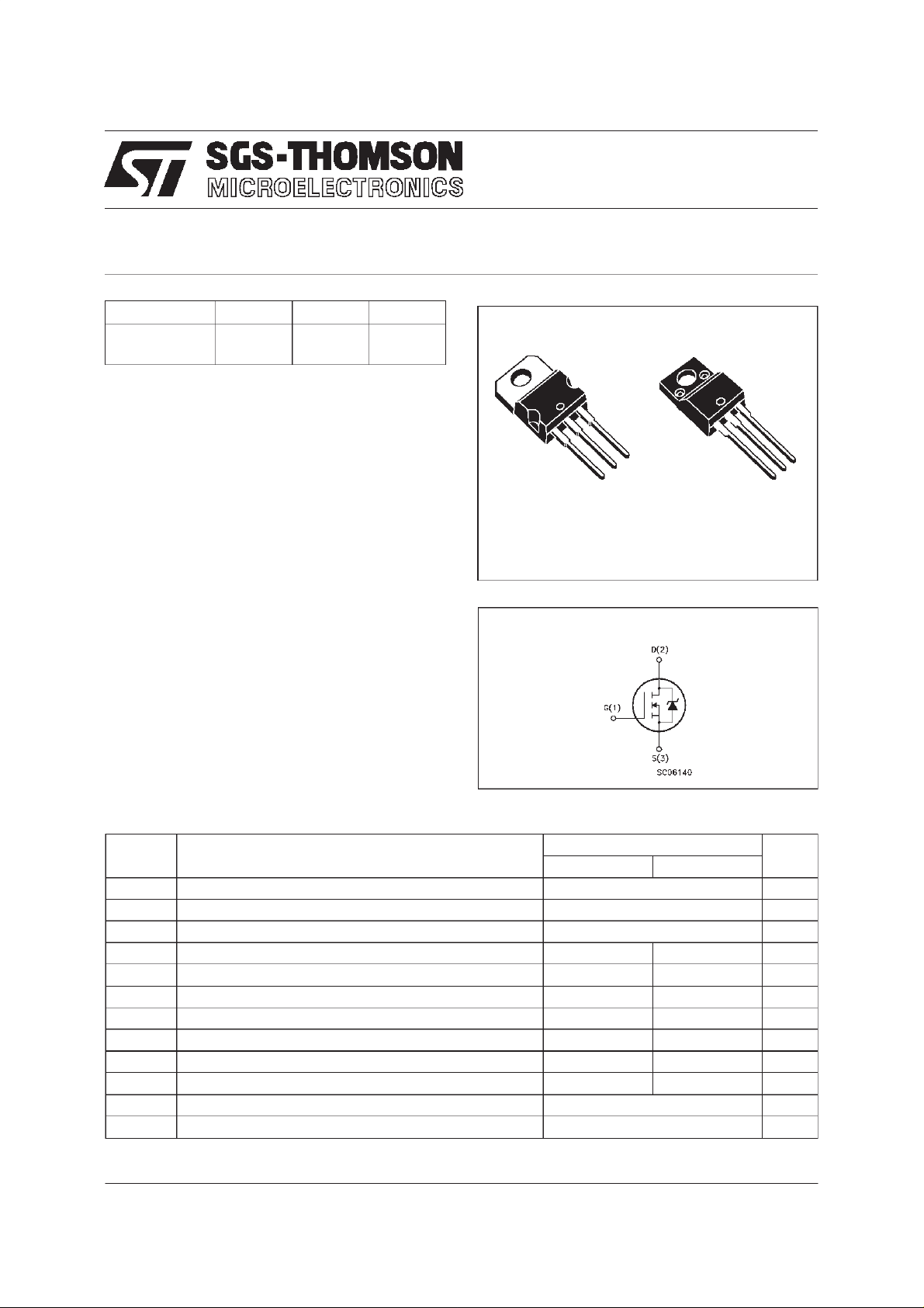
3
2
1
TO-220 TO-220FP
INTERNAL SCHEMATIC DIAGRAM
3
2
1
ABSOLUTE MAXIMUM RATINGS
Symb o l Para meter Value Uni t
ST P6 NB50 ST P6NB 50FP
V
V
V
I
DM
P
dv/dt(
V
T
(•) Pulsewidth limitedby safe operating area (1)ISD≤ 6A, di/dt ≤ 200 A/µs, VDD≤ V
March 1998
Drain-source Voltage (VGS=0) 500 V
DS
Drain- gate Voltage (RGS=20kΩ)
DGR
Gat e- source Volt age ± 30 V
GS
Drain Current (con tinuous) at Tc=25oC5.83.4A
I
D
I
Drain Current (con tinuous) at Tc=100oC3.72.1A
D
500 V
(•) Drain Current (puls ed ) 23.2 23.2 A
Tot al Dissipat i on at Tc=25oC10035W
tot
Derat in g Factor 0.8 0.28 W/
1) Pea k Diode Recovery volt age sl ope 4.5 4.5 V/ns
Ins ulation With st and V oltage (DC) -- 2000
ISO
Sto rage Temper ature -65 to 150
stg
Max. Operat ing J unctio n Temper at u r e 150
T
j
,Tj≤T
(BR)DSS
JMAX
o
C
o
C
o
C
o
C
1/9
Page 2
STP6NB50/FP
THERMAL DATA
TO-220 TO- 220FP
R
thj-case
R
thj-amb
R
thc-sin k
T
AVALANCHE CHARACTERISTICS
Symbol Para met e r Max Value Uni t
I
AR
E
Ther mal Resist ance Junctio n-c a s e Max 1.25 3.57
Ther mal Resist ance Junctio n-ambient Max
Ther mal Resist ance Case-sink T yp
Maximum Lead T e mperat ure For Sold eri ng Pur p os e
l
Avalanche Curre nt , Repet it i v e or Not-Repetitive
(pulse w idth limited by T
Single Pulse Avalanche Energy
AS
(starting T
=25oC, ID=IAR,VDD=50V)
j
max, δ <1%)
j
62.5
0.5
300
5.8 A
290 mJ
o
C/W
o
C/W
o
C/W
o
C
ELECTRICAL CHARACTERISTICS (T
=25oC unlessotherwisespecified)
case
OFF
Symbol Parameter Test Condition s Min. Typ. Max. Unit
V
(BR)DSS
Drain-sourc e
=250µAVGS=0
I
D
500 V
Breakdown Voltage
I
DSS
I
GSS
Zer o Gate Vo lt age
Drain Cur rent (V
GS
Gat e-body Leakage
Current (V
DS
=0)
=0)
=MaxRating
V
DS
V
=MaxRating Tc=125oC
DS
= ± 30 V
V
GS
1
50
± 100 nA
ON (∗)
Symbol Parameter Test Condition s Min. Typ. Max. Unit
V
GS(th )
Gate Threshold
V
DS=VGSID
=250µA
345V
Voltage
R
DS(on)
Stati c Drain-so urce On
VGS=10V ID= 2.9 A 1.35 1.5 Ω
Resistance
I
D(on)
On S tate Drain Cu rr e nt VDS>I
D(on)xRDS(on)max
5.8 A
VGS=10V
DYNAMIC
Symbol Parameter Test Condition s Min. Typ. Max. Unit
g
(∗)Forward
fs
Tr ansconductanc e
C
C
C
Input Capaci tance
iss
Out put C apa citanc e
oss
Reverse Transfer
rss
Capa cit an c e
VDS>I
D(on)xRDS(on)maxID
=2.9A 2.5 4 S
VDS=25V f=1MHz VGS= 0 680
110
12
884
149
16
µA
µA
pF
pF
pF
2/9
Page 3
STP6NB50/FP
ELECTRICAL CHARACTERISTICS (continued)
SWITCHINGON
Symbol Parameter Test Condition s Min. Typ. Max. Unit
t
d(on)
Turn-on Time
r
Rise Time
t
VDD=250V ID=2.9A
=4.7 Ω VGS=10V
R
G
11.5
8
(see test circuit, figure 3)
Q
Q
Q
Total Gate Charge
g
Gat e-Sour ce Charge
gs
Gate-Drain Charge
gd
VDD=400V ID=5.8A VGS=10V 21
7.2
8
SWITCHINGOFF
Symbol Parameter Test Condition s Min. Typ. Max. Unit
t
r(Voff)
t
t
Of f - voltag e Rise Tim e
Fall Time
f
Cross-ov er Tim e
c
VDD=400V ID=5.8A
=4.7 Ω VGS=10V
R
G
(see test circuit, figure 5)
7
5
15
SOURCE DRAIN DIODE
Symbol Parameter Test Condition s Min. Typ. Max. Unit
I
SD
I
SDM
V
SD
t
Q
I
RRM
(∗) Pulsed: Pulse duration =300 µs, duty cycle1.5 %
(•) Pulse width limited by safe operating area
Source-drain Current
(•)
Source-drain Current
(pulsed)
(∗) For ward On Voltage ISD=5.8A VGS=0 1.6 V
Reverse Recovery
rr
Time
Reverse Recovery
rr
= 5.8 A di/dt = 100 A /µs
I
SD
=100V Tj=150oC
V
DD
(see test circuit, figure 5)
435
3.3
Charge
Reverse Recovery
15
Current
16
12
30 nC
12
10
23
5.8
23.2
ns
ns
nC
nC
ns
ns
ns
A
A
ns
µC
A
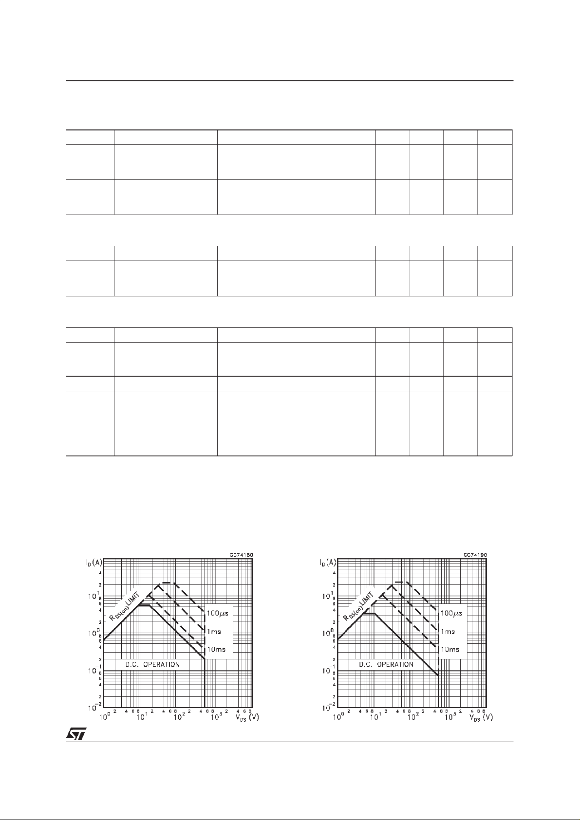
Safe Operating Areafor TO-220 Safe Operating Area for TO-220FP
3/9
Page 4

STP6NB50/FP
ThermalImpedance for TO-220
OutputCharacteristics
ThermalImpedance forTO-220FP
TransferCharacteristics
Transconductance
4/9
StaticDrain-sourceOn Resistance
Page 5

STP6NB50/FP
GateCharge vs Gate-sourceVoltage
Normalized GateThresholdVoltage vs
Temperature
CapacitanceVariations
Normalized On Resistancevs Temperature
Source-drainDiode Forward Characteristics
5/9
Page 6

STP6NB50/FP
Fig. 1: Unclamped InductiveLoad Test Circuit
Fig. 3: SwitchingTimes Test Circuits For
ResistiveLoad
Fig. 2: Unclamped Inductive Waveform
Fig. 4: Gate Chargetest Circuit
Fig. 5: Test Circuit For InductiveLoad Switching
And Diode RecoveryTimes
6/9
Page 7

TO-220 MECHANICAL DATA
STP6NB50/FP
DIM.
MIN. TYP. MAX. MIN. TYP. MAX.
A 4.40 4.60 0.173 0.181
C 1.23 1.32 0.048 0.051
D 2.40 2.72 0.094 0.107
D1 1.27 0.050
E 0.49 0.70 0.019 0.027
F 0.61 0.88 0.024 0.034
F1 1.14 1.70 0.044 0.067
F2 1.14 1.70 0.044 0.067
G 4.95 5.15 0.194 0.203
G1 2.4 2.7 0.094 0.106
H2 10.0 10.40 0.393 0.409
L2 16.4 0.645
L4 13.0 14.0 0.511 0.551
L5 2.65 2.95 0.104 0.116
L6 15.25 15.75 0.600 0.620
L7 6.2 6.6 0.244 0.260
L9 3.5 3.93 0.137 0.154
DIA. 3.75 3.85 0.147 0.151
mm inch
E
A
L4
D
F2
F1
G1
H2
G
F
C
D1
L2
Dia.
L5
L7
L6
L9
P011C
7/9
Page 8

STP6NB50/FP
TO-220FP MECHANICALDATA
DIM.
MIN. TYP. MAX. MIN. TYP. MAX.
A 4.4 4.6 0.173 0.181
B 2.5 2.7 0.098 0.106
D 2.5 2.75 0.098 0.108
E 0.45 0.7 0.017 0.027
F 0.75 1 0.030 0.039
F1 1.15 1.7 0.045 0.067
F2 1.15 1.7 0.045 0.067
G 4.95 5.2 0.195 0.204
G1 2.4 2.7 0.094 0.106
H 10 10.4 0.393 0.409
L2 16 0.630
L3 28.6 30.6 1.126 1.204
L4 9.8 10.6 0.385 0.417
L6 15.9 16.4 0.626 0.645
L7 9 9.3 0.354 0.366
Ø 3 3.2 0.118 0.126
mm inch
E
A
D
B
L3
L6
L7
¯
F1
F
G1
H
G
F2
123
L2
L4
8/9
Page 9

STP6NB50/FP
Information furnished is believed to be accurate and reliable. However, SGS-THOMSON Microelectronics assumes no responsability for the
consequences of use of such information nor for anyinfringementof patents or other rightsof third parties which may results from itsuse. No
license is granted by implication or otherwise underanypatent orpatent rights of SGS-THOMSON Microelectronics. Specifications mentioned
in thispublication are subject to change without notice. This publication supersedes and replaces all information previously supplied.
SGS-THOMSON Microelectronics productsarenot authorizedfor use as critical componentsin life support devices orsystems withoutexpress
written approval ofSGS-THOMSON Microelectonics.
1998 SGS-THOMSON Microelectronics - Printedin Italy - All Rights Reserved
Australia - Brazil - Canada -China - France - Germany - Italy - Japan - Korea - Malaysia - Malta - Morocco - The Netherlands -
Singapore - Spain - Sweden- Switzerland - Taiwan-Thailand - United Kingdom - U.S.A
SGS-THOMSON Microelectronics GROUP OF COMPANIES
...
9/9
 Loading...