

Page 1
STP60NF03L
N-CHANNEL 30V - 0.008
TYPE V
ST P60NF03L 30 V < 0. 010 Ω 60 A
■ TYPICALR
■ LOW THRESHOLDDRIVE
DS(on)
DSS
= 0.008 Ω
DESCRIPTION
This Power Mosfet is the latest development of
STMicroelectronics unique ”Single Feature
Size” strip-based process. The resulting
transistor shows extremely high packing density
for low on-resistance, rugged avalance
characteristics and less critical alignment steps
therefore a remarkable manufacturing
reproducibility.
APPLICATIONS
■ HIGHCURRENT, HIGH SPEEDSWITCHING
■ MOTORCONTROL, AUDIOAMPLIFIERS
■ DC-DC& DC-AC CONVERTERS
■ AUTOMOTIVEENVIRONMENT(INJECTION,
ABS, AIR-BAG, LAMPDRIVERS,Etc. )
R
DS(on)
I
D
Ω
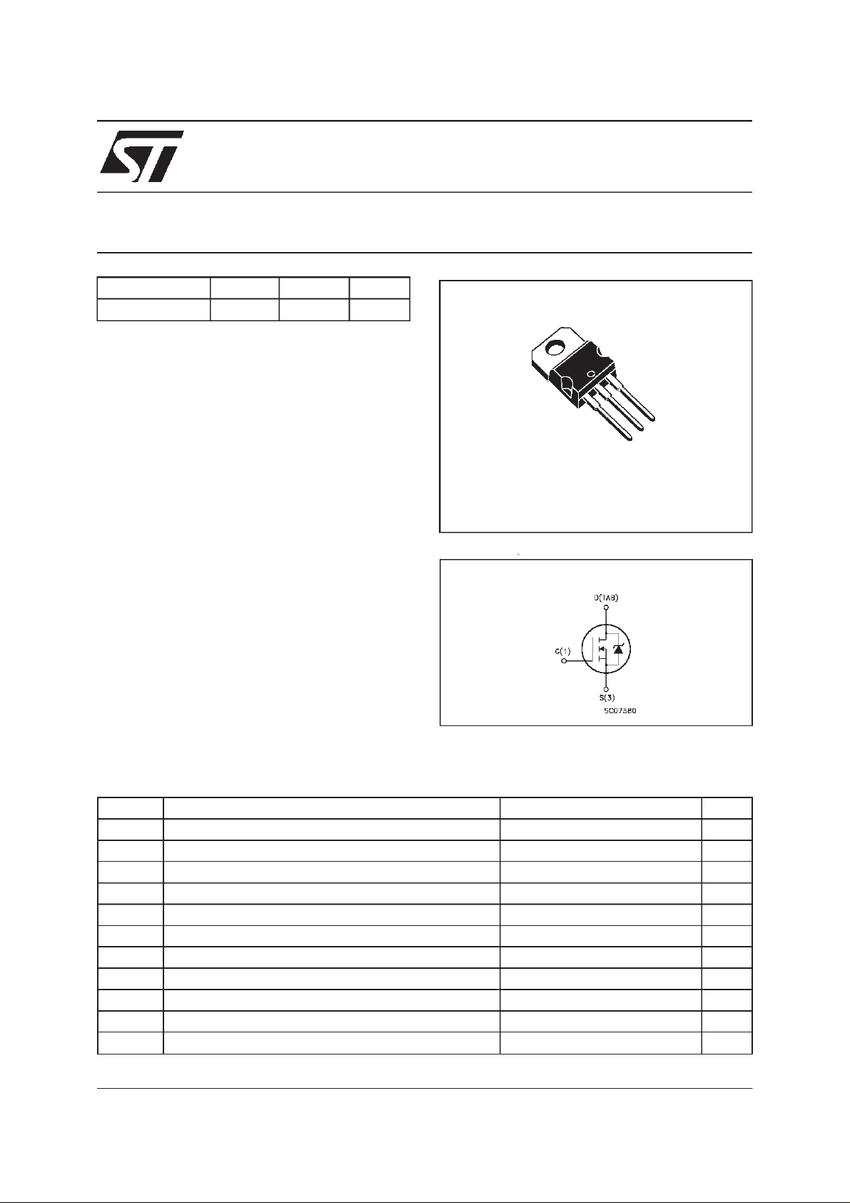
- 60A TO-220
STripFET POWER MOSFET
PRELIMINARY DATA
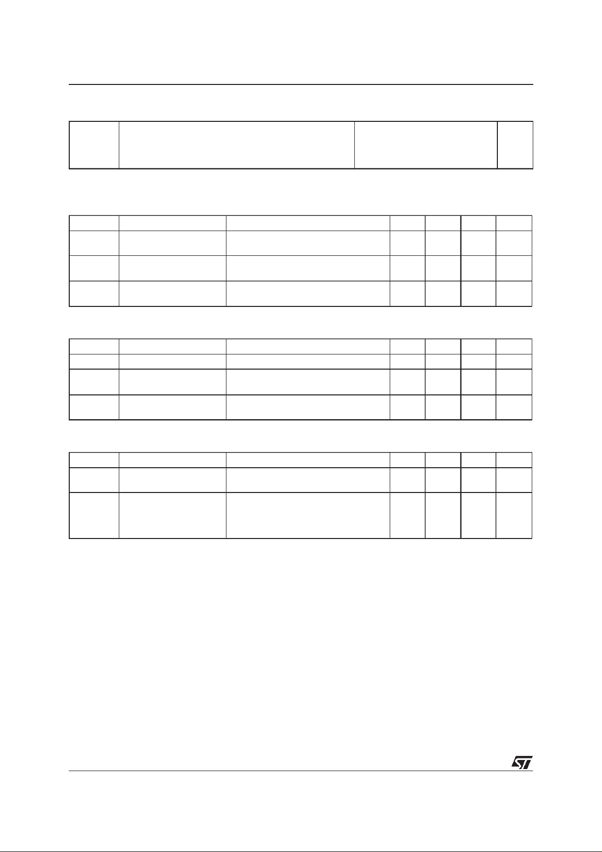
3
2
1
TO-220
INTERNAL SCHEMATIC DIAGRAM
ABSOLUTE MAXIMUM RATINGS
Symbol Parameter Value Unit
V
V
V
I
DM
P
E
AS(1
T
(•) Pulse width limited by safe operating area (1) starting Tj
September 1999
Dra in- sour c e Volt age ( VGS=0) 30 V
DS
Dra in- gate V ol t age (RGS=20kΩ)30V
DGR
Gat e-source Voltage
GS
I
Dra in Current ( continuous) at Tc=25oC60A
D
I
Dra in Current ( continuous) at Tc=100oC42A
D
(•) D rain Current (pulsed) 240 A
Tot al Dissipat ion at Tc=25oC 100 W
tot
Der ati ng Fac t or 0.67 W/
) Single Pulse Avalanche Energy 650 mJ
St orage Temper at ure -65 t o 175
stg
T
Max. O perating Junc t ion T emperatur e 175
j
=25oC,ID=30A,VDD= 20V
20 V
±
o
C
o
C
o
C
1/6
Page 2
STP60NF03L
THERMAL DATA
R
thj-case
Rthj-amb
R
thc-sink
T
Ther mal Resistanc e Junct ion-case Max
Ther mal Resistanc e Junct ion-ambient Max
Ther mal Resistanc e Case-sink Ty p
Maximum Lead Temperature For Soldering Purpos e
l
1.5
62.5
0.5
300
o
C/W
oC/W
o
C/W
o
C
ELECTRICAL CHARACTERISTICS
=25oC unless otherwisespecified)
(T
case
OFF
Symbol Parameter Test Conditions Min. Typ. Max. Unit
V
(BR)DSS
Drain-source
ID=250µAVGS=0 30 V
Break dow n V o lt age
I
DSS
I
GSS
Zero Gate Voltage
Drain Curr e nt (V
GS
Gat e- bod y Leak ag e
Current (V
DS
=0)
=0)
V
=MaxRating
DS
=MaxRating Tc=125oC
V
DS
V
= ± 20 V ± 100 nA
GS
1
10
ON(∗)
Symbol Parameter Test Conditions Min. Typ. Max. Unit
V
GS(th)
R
DS(on)
I
D(on)
Gate Threshold Voltage VDS=VGSID= 250 µA11.52.5V
Sta t ic Drain-s ource On
Resistance
VGS=10V ID=30A
=4.5V ID=30A
V
GS
On State Drain Current VDS>I
D(on)xRDS(on)max
0.008
0.0095
60 A
0.010
0.015ΩΩ
VGS=10V
DYNAMIC
Symbol Parameter Test Conditions Min. Typ. Max. Unit
g
(∗)Forward
fs
Tr ansc on duc tance
C
C
C
Input Capacitance
iss
Out put Capac it ance
oss
Reverse Tr ansfer
rss
Capacit a nc e
VDS>I
D(on)xRDS(on)maxID
=30 A 60 S
VDS=25V f=1MHz VGS= 0 2550
630
215
µ
µA
pF
pF
pF
A
2/6
Page 3

STP60NF03L
ELECTRICAL CHARACTERISTICS
(continued)
SWITCHING ON
Symbol Parameter Test Conditions Min. Typ. Max. Unit
t
d(on)
t
Tur n-on Delay Time
Rise Tim e
r
VDD=15V ID=30A
R
=4.7
G
Ω
VGS=4.5V
40
250
(Resis t iv e Load, see f ig. 3)
Q
Q
Q
Tot al Gat e Charge
g
Gat e- Source Charge
gs
Gate-Drain Charge
gd
VDD=24V ID=60A VGS=5V 43
12
21
58 nC
SWITCHING OFF
Symbol Parameter Test Conditions Min. Typ. Max. Unit
t
d(off)
Tur n-of f Dela y Time
t
Fall T ime
f
VDD=15V ID=30A
=4.7 Ω VGS=4.5V
R
G
60
70
(Resis t iv e Load, see f ig. 3)
SOURCEDRAINDIODE
Symbol Parameter Test Conditions Min. Typ. Max. Unit
I
SDM
V
I
SD
Q
I
RRM
SD
t
Source-drain Current
(•)
Source-drain Current
60
240
(pulsed)
(∗)ForwardOnVoltage ISD=60A VGS=0 1.5 V
Reverse Recovery
rr
Time
Reverse Recovery
rr
ISD= 60 A di/dt = 100 A/µs
=15V Tj=150oC
V
DD
(see test circuit, fig. 5)
75
100
Charge
Reverse Recovery
2.6
Current
ns
ns
nC
nC
ns
ns
A
A
ns
nC
A
(∗) Pulsed: Pulse duration = 300 µs, duty cycle 1.5 %
(•) Pulse width limited by safe operatingarea
3/6
Page 4

STP60NF03L
Fig. 1:
UnclampedInductiveLoad TestCircuit
Fig. 3: SwitchingTimes Test Circuits For
ResistiveLoad
Fig. 2:
UnclampedInductive Waveform
Fig. 4: Gate Chargetest Circuit
Fig. 5:
Test CircuitFor InductiveLoad Switching
And Diode Recovery Times
4/6
Page 5

TO-220 MECHANICAL DATA
STP60NF03L
DIM.
MIN. TYP. MAX. MIN. TYP. MAX.
A 4.40 4.60 0.173 0.181
C 1.23 1.32 0.048 0.051
D 2.40 2.72 0.094 0.107
D1 1.27 0.050
E 0.49 0.70 0.019 0.027
F 0.61 0.88 0.024 0.034
F1 1.14 1.70 0.044 0.067
F2 1.14 1.70 0.044 0.067
G 4.95 5.15 0.194 0.203
G1 2.4 2.7 0.094 0.106
H2 10.0 10.40 0.393 0.409
L2 16.4 0.645
L4 13.0 14.0 0.511 0.551
L5 2.65 2.95 0.104 0.116
L6 15.25 15.75 0.600 0.620
L7 6.2 6.6 0.244 0.260
L9 3.5 3.93 0.137 0.154
DIA. 3.75 3.85 0.147 0.151
mm inch
E
A
L4
D
F2
F1
G1
H2
G
F
P011C
C
D1
L2
Dia.
L5
L7
L6
L9
5/6
Page 6

STP60NF03L
Information furnishedis believedto be accurateand reliable.However, STMicroelectronics assumes no responsibilityfor the consequences
of use of such information nor for any infringement of patents or other rights of third parties which may result from its use. No licenseis
granted by implication or otherwise under any patent or patent rights ofSTMicroelectronics. Specificationmentioned in this publication are
subjectto change without notice.Thispublicationsupersedes and replacesall informationpreviouslysupplied. STMicroelectronicsproducts
are not authorized for use as critical components in life support devicesor systemswithout express written approvalof STMicroelectronics.
The STlogo is a trademark of STMicroelectronics
1999 STMicroelectronics – Printed in Italy – All Rights Reserved
STMicroelectronics GROUP OF COMPANIES
Australia - Brazil - China - Finland - France - Germany - Hong Kong - India - Italy - Japan - Malaysia - Malta - Morocco -
6/6
Singapore - Spain - Sweden - Switzerland - United Kingdom - U.S.A.
http://www.st.com
.
 Loading...