

Page 1
STP60NE06L-16
N - CHANNEL 60V - 0.014Ω - 60A TO-220/TO-220FP
TYPE V
ST P60NE06L-16
ST P60NE06L-16F P
■ TYPICALR
■ AVALANCHERUGGEDTECHNOLOGY
■ LOW GATE CHARGE
■ HIGHCURRENT CAPABILITY
■ 175
■ LOW THRESHOLDDRIVE
o
DS(on)
C OPERATINGTEMPERATURE
DSS
60 V
60 V
= 0.014 Ω
DESCRIPTION
This Power Mosfet is the latest development of
STMicroelectronisunique ”Single Feature Size”
strip-based process. The resulting transistor
shows extremely high packing density for low onresistance, rugged avalanche characteristicsand
less critical alignment steps therefore a remarkable manufacturingreproducibility.
R
DS(on)
<0.016Ω
<0.016Ω
I
D
60 A
35 A
STP60NE06L-16FP
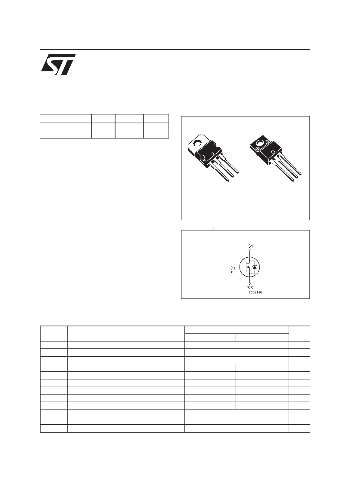
STripFET POWER MOSFET
3
2
1
TO-220 TO-220FP
INTERNAL SCHEMATIC DIAGRAM
3
2
1
APPLICATIONS
■ HIGHCURRENT, HIGH SPEED SWITCHING
■ SOLENOIDAND RELAYDRIVERS
■ DC-DC& DC-ACCONVERTERS
■ AUTOMOTIVEENVIRONMENT
ABSOLUTE MAXIMUM RATINGS
Symbol Parameter Value Unit
STP 60NE06L- 16 STP 60NE 0 6L - 16 F P
V
V
V
I
DM
P
V
dv/ dt Peak Diode Recovery voltage slope 6 V/ ns
T
(•) Pulsewidth limited by safeoperating area (1)ISD≤ 60 A, di/dt ≤ 300 A/µs, VDD≤ V
May 2000
Drain-source Voltage (VGS=0) 60 V
DS
Drain- gate Voltage (RGS=20kΩ)60V
DGR
Gate-source Voltage ± 15 V
GS
I
Drain Curre nt (cont i nuous) at Tc=25oC60 35A
D
Drain Curre nt (cont i nuous) at Tc=100oC42 24A
I
D
(•) Drain Curre nt (pulse d) 240 140 A
Total Dissipation at Tc=25oC15045W
tot
Derat ing F ac tor 1 0.3 W/
Ins ulat ion W i th s t and Voltage (DC) 2 000 V
ISO
Sto rage Temperat ure -65 to 175
stg
T
Max. Operat ing Junction Tempera t ure 175
j
(BR)DSS,Tj≤TJMAX
o
C
o
C
o
C
1/9
Page 2
STP60NE06L-16/FP
THERMAL DATA
TO-220 TO-220FP
R
thj-case
R
thj-amb
R
thc-sink
T
AVALANCHE CHARACTERISTICS
Symbol Parameter Max V alue Unit
I
AR
E
Ther mal Resistanc e Junct ion-case Max 0.94 2.7
Ther mal Resistanc e Junct ion-ambient Max
Ther mal Resistanc e Case-sink Ty p
Maximum L ead Temperature F or Solder ing P urp os e
l
Avalanche Current, R epetitive or Not-Repetitive
(pulse width limited by T
Single Pul se Avalanche Ener gy
AS
(starting T
=25oC, ID=IAR,VDD=25V)
j
max)
j
62.5
0.5
300
60 A
400 mJ
o
C/W
o
C/W
o
C/W
o
C
ELECTRICAL CHARACTERISTICS
=25oC unless otherwisespecified)
(T
case
OFF
Symbol Parameter Test Conditions Min. Typ. Max. Unit
V
(BR)DSS
Drain-source
ID=250µAVGS=0 60 V
Break dow n Vo lt age
I
DSS
I
GSS
Zero Gate Voltage
Drain Curre nt (V
GS
Gat e- bod y Leakag e
Current (V
DS
=0)
=0)
V
=MaxRating
DS
=MaxRating Tc= 125oC
V
DS
V
=± 15 V
GS
1
10
100 nA
±
ON (∗)
Symbol Parameter Test Conditions Min. Typ. Max. Unit
V
GS(th)
R
DS(on)
I
D(on)
Gate Threshold Volt age VDS=VGSID= 250µA11.62.5V
Sta t ic Drain-s our c e On
Resistance
VGS=5V ID=30A
=10V ID=30A
V
GS
On State Drain Current VDS>I
D(on)xRDS(on )max
0.014
0.012
60 A
0.016
0.014ΩΩ
VGS=10V
DYNAMIC
Symbol Parameter Test Conditions Min. Typ. Max. Unit
g
(∗)Forward
fs
Tr ansc on duc tance
C
C
C
Input Capaci t ance
iss
Out put Capac itance
oss
Reverse Transfer
rss
Capacit a nc e
VDS>I
D(on)xRDS(on )maxID
=30 A 30 S
VDS=25V f=1MHz VGS= 0 4150
590
150
µA
µA
pF
pF
pF
2/9
Page 3
STP60NE06L-16/FP
ELECTRICAL CHARACTERISTICS
(continued)
SWITCHING ON
Symbol Parameter Test Conditions Min. Typ. Max. Unit
t
d(on)
t
Tur n-on Delay Time
Rise Time
r
VDD=30V ID=30A
R
=4.7
G
Ω
VGS=5V
50
155
(Resis t iv e Load, see fig. 3)
Q
Q
Q
Tot al Gate Charge
g
Gat e- Source Charge
gs
Gate-Drain Charge
gd
VDD=40V ID=60A VGS=5V 55
15
30
70 nC
SWITCHING OFF
Symbol Parameter Test Conditions Min. Typ. Max. Unit
t
d(off)
Tur n-of f Dela y Tim e
t
Fall T ime
f
VDD=30V ID=30A
R
G
=4.7
Ω
VGS=5V
125
25
(Resis t iv e Load, see fig. 3)
t
r(Voff)
t
t
Off-volt age Rise Time
Fall T ime
f
Cross-over Tim e
c
VDD=48V ID=20A
R
=4.7
G
Ω
VGS=5V
(Indu ct iv e Load, see fig . 5)
45
220
280
SOURCEDRAINDIODE
Symbol Parameter Test Conditions Min. Typ. Max. Unit
I
SD
I
SDM
V
SD
t
Q
I
RRM
(∗) Pulsed:Pulse duration = 300µs, duty cycle 1.5%
(•) Pulse width limited by safeoperating area
Source-drain Current
(•)
Source-drain Current
60
240
(pulsed)
(∗)ForwardOnVoltage ISD=60A VGS=0 1.5 V
Reverse Recovery
rr
Time
Reverse Recovery
rr
ISD= 60 A di/dt = 100 A/µs
=30V TJ=150oC
V
DD
(see test circuit, fig. 5)
85
300
Charge
Reverse Recovery
7
Current
ns
ns
nC
nC
ns
ns
ns
ns
ns
A
A
ns
µ
A
C
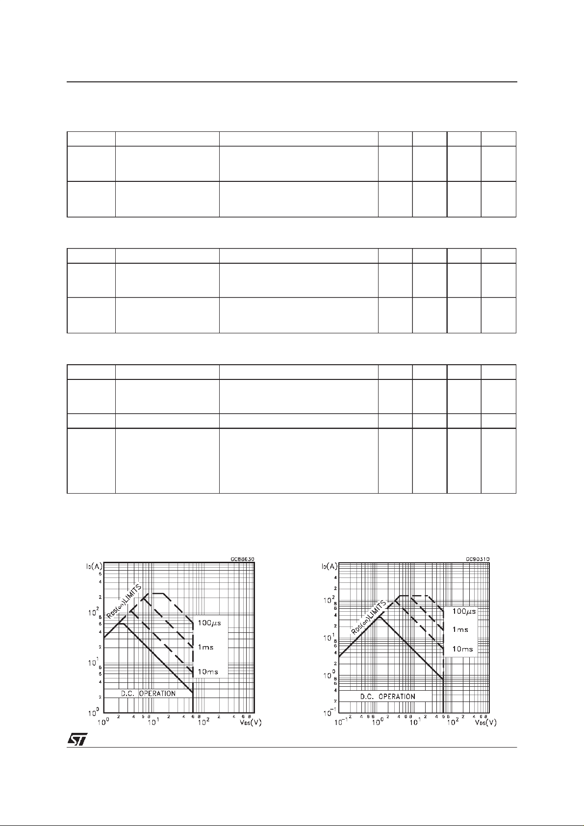
SafeOperating Area for TO-220 SafeOperating Area for TO-220FP
3/9
Page 4

STP60NE06L-16/FP
ThermalImpedancefor TO-220
OutputCharacteristics
ThermalImpedanceforTO-220FP
TransferCharacteristics
Transconductance
4/9
Static Drain-sourceOn Resistance
Page 5

STP60NE06L-16/FP
Gate Charge vs Gate-sourceVoltage
NormalizedGate ThresholdVoltage vs
Temperature
CapacitanceVariations
NormalizedOn Resistancevs Temperature
Source-drainDiode Forward Characteristics
5/9
Page 6

STP60NE06L-16/FP
Fig. 1
: UnclampedInductiveLoad TestCircuit
Fig. 3: SwitchingTimesTest CircuitsFor
ResistiveLoad
Fig. 2
: UnclampedInductive Waveform
Fig. 4: GateCharge testCircuit
Fig. 5
: TestCircuitFor InductiveLoad Switching
And Diode Recovery Times
6/9
Page 7

TO-220 MECHANICALDATA
STP60NE06L-16/FP
DIM.
MIN. TYP. MAX. MIN. TYP. MAX.
A 4.40 4.60 0.173 0.181
C 1.23 1.32 0.048 0.051
D 2.40 2.72 0.094 0.107
D1 1.27 0.050
E 0.49 0.70 0.019 0.027
F 0.61 0.88 0.024 0.034
F1 1.14 1.70 0.044 0.067
F2 1.14 1.70 0.044 0.067
G 4.95 5.15 0.194 0.203
G1 2.4 2.7 0.094 0.106
H2 10.0 10.40 0.393 0.409
L2 16.4 0.645
L4 13.0 14.0 0.511 0.551
L5 2.65 2.95 0.104 0.116
L6 15.25 15.75 0.600 0.620
L7 6.2 6.6 0.244 0.260
L9 3.5 3.93 0.137 0.154
DIA. 3.75 3.85 0.147 0.151
mm inch
E
A
L4
D
F2
F1
G1
H2
G
F
P011C
C
D1
L2
Dia.
L5
L7
L6
L9
7/9
Page 8

STP60NE06L-16/FP
TO-220FP MECHANICAL DATA
DIM.
MIN. TYP. MAX. MIN. TYP. MAX.
A 4.4 4.6 0.173 0.181
B 2.5 2.7 0.098 0.106
D 2.5 2.75 0.098 0.108
E 0.45 0.7 0.017 0.027
F 0.75 1 0.030 0.039
F1 1.15 1.7 0.045 0.067
F2 1.15 1.7 0.045 0.067
G 4.95 5.2 0.195 0.204
G1 2.4 2.7 0.094 0.106
H 10 10.4 0.393 0.409
L2 16 0.630
L3 28.6 30.6 1.126 1.204
L4 9.8 10.6 0.385 0.417
L6 15.9 16.4 0.626 0.645
L7 9 9.3 0.354 0.366
Ø 3 3.2 0.118 0.126
mm inch
E
A
D
B
L3
L6
L7
¯
F1
F
G1
H
G
F2
123
L2
L4
8/9
Page 9

STP60NE06L-16/FP
Information furnished is believed to be accurate and reliable. However, STMicroelectronics assumes no responsibility forthe consequences
of use of such information nor for any infringement of patents or other rights of third parties which may result from its use. No license is
granted by implication or otherwise under any patent or patent rights of STMicroelectronics. Specification mentioned in thispublication are
subject to change withoutnotice. Thispublication supersedes and replaces allinformation previously supplied. STMicroelectronics products
are not authorized for use as critical components in life support devices orsystems without express written approval ofSTMicroelectronics.
The ST logo is a trademarkof STMicroelectronics
2000 STMicroelectronics – Printedin Italy –All Rights Reserved
STMicroelectronics GROUP OF COMPANIES
Australia - Brazil -China - Finland- France- Germany -Hong Kong - India- Italy- Japan - Malaysia- Malta -Morocco -
Singapore - Spain - Sweden -Switzerland -United Kingdom- U.S.A.
http://www.st.com
9/9
 Loading...