

Page 1
STP60NE06-16
STP60NE06-16FP
N - CHANNEL ENHANCEMENT MODE
” SINGLEFEATURE SIZE ” POWER MOSFET
TYPE V
STP 60NE06-16
STP 60NE06-16F P
■ TYPICALR
■ EXCEPTIONALdV/dt CAPABILTY
■ 100% AVALANCHETESTED
■ LOW GATE CHARGE 100
■ HIGH dV/dt CAPABILITY
■ APPLICATIONORIENTED
DS(on)
DSS
60 V
60 V
=0.013 Ω
R
DS(on)
<0.016Ω
<0.016Ω
o
C
I
D
60 A
35 A
CHARACTERIZATION
DESCRIPTION
This Power Mosfet is the latest development of
SGS-THOMSON unique ”Single Feature Size”
process whereby a single body is implanted on a
strip layout structure. The resulting transistor
shows extremely high packing density for low onresistance, rugged avalanche characteristics and
less critical alignment steps therefore a remarkable manufacturingreproducibility.
APPLICATIONS
■ DC MOTOR CONTROL
■ DC-DC& DC-AC CONVERTERS
■ SYNCHRONOUS RECTIFICATION
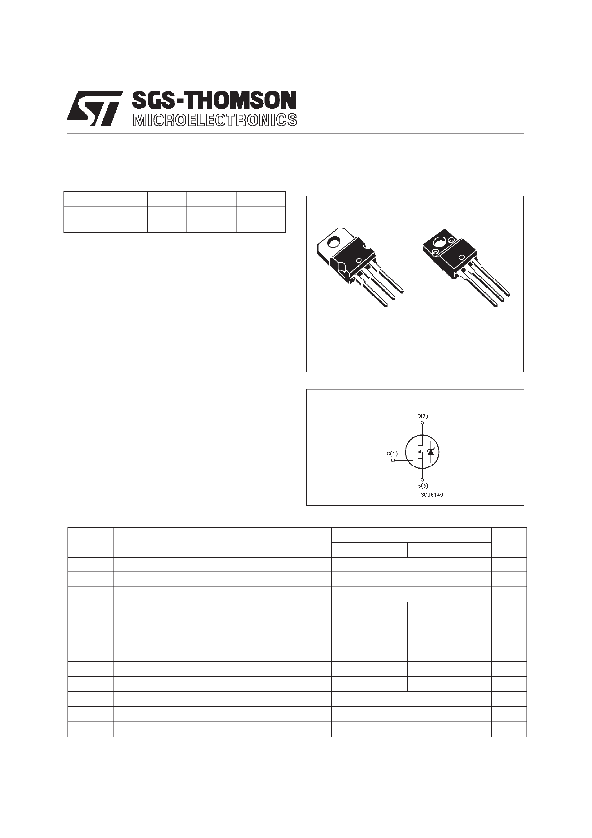
3
2
1
TO-220 TO220FP
INTERNAL SCHEMATIC DIAGRAM
3
2
1
ABSOLUTE MAXIMUM RATINGS
Symbol Parameter Value Unit
STP60NE06-16 STP60NE06-16FP
V
V
V
I
DM
P
V
dV/ dt Peak Diod e Rec ov ery voltage slop e 6 V/ns
T
(•) Pulse width limitedby safe operating area (1)ISD≤ 60 A,di/dt ≤ 300 A/µs, VDD≤ V
December 1997
Drain-s ource Voltage (VGS=0) 60 V
DS
Drain- gate Voltage (RGS=20kΩ)
DGR
Gate-source Voltage ± 20 V
GS
I
Drain Current (co nt inu ous) at Tc=25oC6035A
D
I
Drain Current (co nt inu ous) at Tc=100oC4224A
D
60 V
(•) Drain Current (puls ed) 240 240 A
Tot al D i ss ipa t ion at Tc=25oC 150 40 W
tot
Derat ing Fact or 1 0.3 W/
Insulation W ithstand Voltage (DC) 2000 V
ISO
Sto rage Temper at ure -65 t o 175
stg
T
Max. O per ating J unc t i on Temper at u re 175
j
(BR)DSS,Tj≤TJMAX
o
C
o
C
o
C
1/9
Page 2
STP60NE06-16/FP
THERMAL DATA
TO - 2 20 TO - 220FP
R
thj-case
R
thj-amb
R
thc-sin k
T
AVALANCHE CHARACTERISTICS
Symb o l Parameter Max Value Uni t
I
AR
E
Ther mal Resistance Ju nc t io n- case Max 1 3.75
Ther mal Resistance Ju nc t io n- ambient Max
Ther mal Resistance Ca s e-sink Typ
Maximum Lead Tem p er at u r e Fo r Soldering Purpose
l
Avalanche Curr ent, Repetit iv e or Not-Repetit ive
(pulse width limi t ed by T
Single Pulse Aval anche Energ y
AS
(starti ng T
=25oC, ID=IAR,VDD=25V)
j
max, δ <1%)
j
62.5
0.5
300
60 A
350 mJ
o
C/W
o
C/W
o
C/W
o
C
ELECTRICAL CHARACTERISTICS (T
=25oC unlessotherwisespecified)
case
OFF
Symbol Paramet er Test Cond itions Min. Typ . Max. Unit
V
(BR)DSS
Drain-source
= 250 µAVGS=0
I
D
60 V
Break dow n Voltage
I
DSS
I
GSS
Zero Gate Voltage
Drain Current (V
GS
Gat e- bod y Le akage
Current (V
DS
=0)
=0)
=MaxRating
V
DS
V
=MaxRating Tc=125oC
DS
= ± 20 V
V
GS
1
10
± 100 nA
ON (∗)
Symbol Paramet er Test Cond itions Min. Typ . Max. Unit
V
GS(th )
R
DS(on)
Gat e Thr e shold Voltage
St at ic D rain-source O n
V
DS=VGSID
=250µA
VGS= 10V ID=30A 0.013 0.016 Ω
234V
Resistance
I
D(on)
On State Drain Curr ent VDS>I
D(on)xRDS(on)max
60 A
VGS=10V
DYNAMIC
Symbol Paramet er Test Cond itions Min. Typ . Max. Unit
g
(∗)Forward
fs
Tr ansc on ductance
C
C
C
Input Capacitanc e
iss
Out put Ca pac itance
oss
Reverse Tr ansfer
rss
Capacit a nc e
VDS>I
D(on)xRDS(on)maxID
=30 A 20 35 S
VDS=25V f=1MHz VGS= 0 4600
580
140
6200
800
200
µA
µA
pF
pF
pF
2/9
Page 3
STP60NE06-16/FP
ELECTRICAL CHARACTERISTICS (continued)
SWITCHINGON
Symbol Paramet er Test Cond itions Min. Typ . Max. Unit
t
d(on)
t
Q
Q
Q
SWITCHINGOFF
Symbol Paramet er Test Cond itions Min. Typ . Max. Unit
t
r(Voff)
t
SOURCE DRAIN DIODE
Symbol Paramet er Test Cond itions Min. Typ . Max. Unit
I
SD
I
SDM
V
SD
t
Q
I
RRM
(∗) Pulsed: Pulse duration =300 µs, duty cycle 1.5 %
(•) Pulse width limited by safe operating area
Turn-on Time
Rise T ime
r
Tot al Gate Char ge
g
Gate-Source Charge
gs
Gat e- Drain Charge
gd
Off -voltage R ise Time
t
Fall T ime
f
Cross-over Time
c
Source-drain Current
(•)
Source-drain Current
VDD=30V ID=30A
R
=4.7 W VGS=10V
G
40
12560180
VDD=48V ID=60A VGS= 10 V 115
25
40
VDD=48V ID=60A
=4.7 Ω VGS=10V
R
G
15
150
180
160 nC
25
210
260
60
240
(pulsed)
(∗)ForwardOnVoltage ISD=60A VGS=0 1.5 V
Reverse Recov ery
rr
Time
Reverse Recov ery
rr
= 60 A di/ dt = 100 A/µs
I
SD
=30V Tj= 150oC
V
DD
100
0.4
Charge
Reverse Recov ery
8
Current
ns
ns
nC
nC
ns
ns
ns
A
A
ns
µC
A
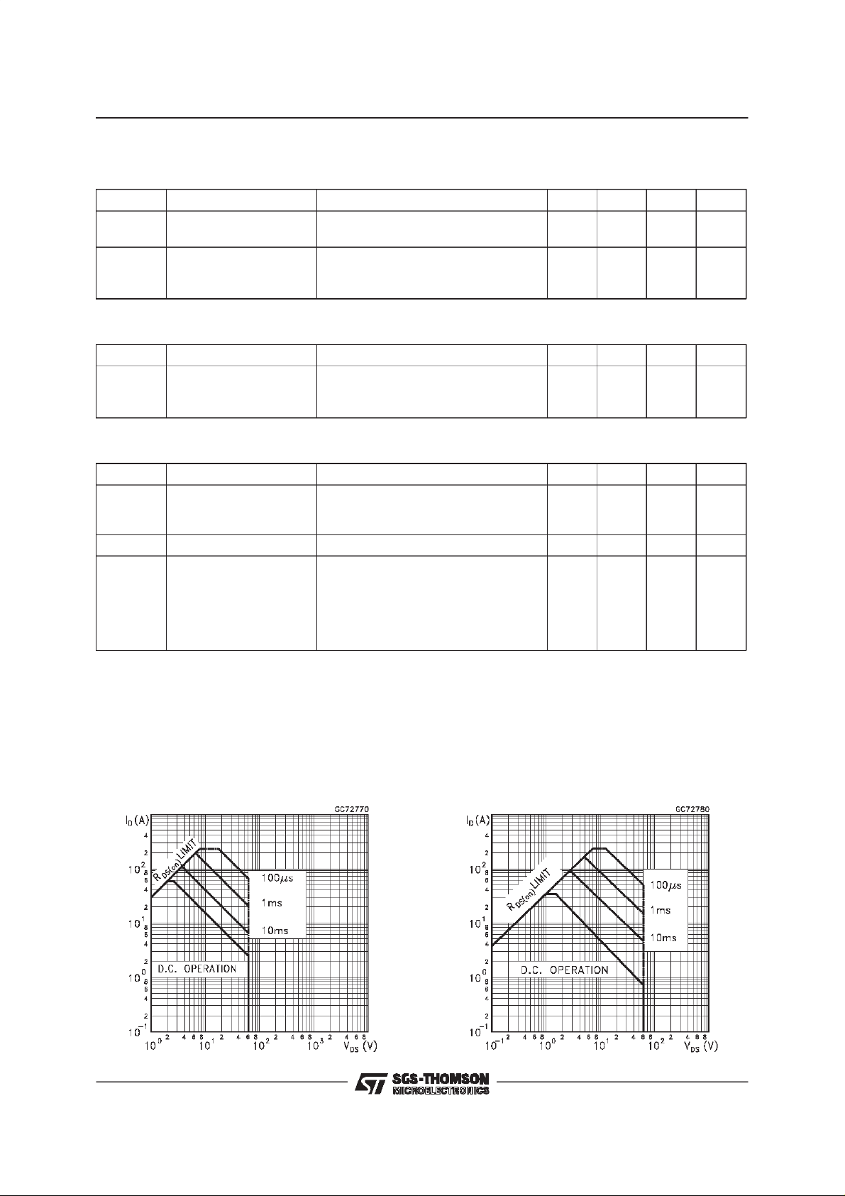
Safe Operating Areafor TO-220 Safe Operating Area for TO-220FP
3/9
Page 4

STP60NE06-16/FP
Thermal Impedancefor TO-220
OutputCharacteristics
ThermalImpedanceforTO-220FP
TransferCharacteristics
Transconductance
4/9
StaticDrain-SourceOnResistance
Page 5

STP60NE06-16/FP
GateCharge vs Gate-SourceVoltage
Normalized Gate ThresholdVoltage vs
Temperature
CapacitanceVariations
Normalized On Resistance vs Temperature
Source-DrainDiode ForwardCharacteristics
5/9
Page 6

STP60NE06-16/FP
Fig. 1: Unclamped InductiveLoad Test Circuit
Fig. 3: SwitchingTimes Test Circuits For
ResistiveLoad
Fig. 2: Unclamped InductiveWaveform
Fig. 4: Gate Chargetest Circuit
Fig. 5: Test Circuit For InductiveLoad Switching
And Diode RecoveryTimes
6/9
Page 7

TO-220 MECHANICAL DATA
STP60NE06-16/FP
DIM.
MIN. TYP. MAX. MIN. TYP. MAX.
A 4.40 4.60 0.173 0.181
C 1.23 1.32 0.048 0.051
D 2.40 2.72 0.094 0.107
D1 1.27 0.050
E 0.49 0.70 0.019 0.027
F 0.61 0.88 0.024 0.034
F1 1.14 1.70 0.044 0.067
F2 1.14 1.70 0.044 0.067
G 4.95 5.15 0.194 0.203
G1 2.4 2.7 0.094 0.106
H2 10.0 10.40 0.393 0.409
L2 16.4 0.645
L4 13.0 14.0 0.511 0.551
L5 2.65 2.95 0.104 0.116
L6 15.25 15.75 0.600 0.620
L7 6.2 6.6 0.244 0.260
L9 3.5 3.93 0.137 0.154
DIA. 3.75 3.85 0.147 0.151
mm inch
E
A
L4
D
F2
F1
G1
F
H2
G
C
D1
L2
Dia.
L5
L7
L6
L9
P011C
7/9
Page 8

STP60NE06-16/FP
TO-220FP MECHANICALDATA
DIM.
MIN. TYP. MAX. MIN. TYP. MAX.
A 4.4 4.6 0.173 0.181
B 2.5 2.7 0.098 0.106
D 2.5 2.75 0.098 0.108
E 0.45 0.7 0.017 0.027
F 0.75 1 0.030 0.039
F1 1.15 1.7 0.045 0.067
F2 1.15 1.7 0.045 0.067
G 4.95 5.2 0.195 0.204
G1 2.4 2.7 0.094 0.106
H 10 10.4 0.393 0.409
L2 16 0.630
L3 28.6 30.6 1.126 1.204
L4 9.8 10.6 0.385 0.417
L6 15.9 16.4 0.626 0.645
L7 9 9.3 0.354 0.366
Ø 3 3.2 0.118 0.126
mm inch
E
A
D
B
L3
L6
L7
¯
F1
F
G1
H
G
F2
123
L2
L4
8/9
Page 9

STP60NE06-16/FP
Information furnishedis believed to be accurate and reliable. However,SGS-THOMSON Microelectronics assumes no responsability forthe
consequencesof use of such information nor for any infringement of patents or otherrights of third parties whichmay results from its use. No
licenseis granted by implicationor otherwise underany patentor patentrights ofSGS-THOMSONMicroelectronics. Specifications mentioned
in this publicationare subject to change without notice. This publication supersedes and replacesall information previously supplied.
SGS-THOMSONMicroelectronics productsarenotauthorizedfor useascriticalcomponents in lifesupportdevicesor systemswithoutexpress
writtenapproval of SGS-THOMSONMicroelectonics.
1997 SGS-THOMSONMicroelectronics- Printedin Italy - AllRights Reserved
Australia- Brazil- Canada - China - France - Germany - Italy - Japan - Korea - Malaysia - Malta- Morocco - The Netherlands-
Singapore- Spain- Sweden- Switzerland - Taiwan - Thailand - United Kingdom - U.S.A
SGS-THOMSONMicroelectronicsGROUP OF COMPANIES
...
9/9
 Loading...