

Page 1
STP5NB60
N - CHANNEL 600V - 1.8Ω - 5A - TO-220/TO-220FP
TYPE V
STP5NB60
STP5NB60 FP
■ TYPICALR
■ EXTREMELYHIGH dv/dt CAPABILITY
■ 100%AVALANCHETESTED
■ VERYLOW INTRINSIC CAPACITANCES
■ GATECHARGE MINIMIZED
DS(on)
DSS
600 V
600 V
= 1.8
DESCRIPTION
Using the latest high voltageMESH OVERLAY
process, STMicroelectronics has designed an
advanced family of power MOSFETs with
outstanding performances. The new patent
pending strip layout coupled with the Company’s
proprietary edge termination structure, gives the
lowest RDS(on) per area, exceptional avalanche
and dv/dt capabilities and unrivalled gate charge
and switching characteristics.
Ω
R
DS(on)
<2.0Ω
<2.0
Ω
I
D
5A
3A
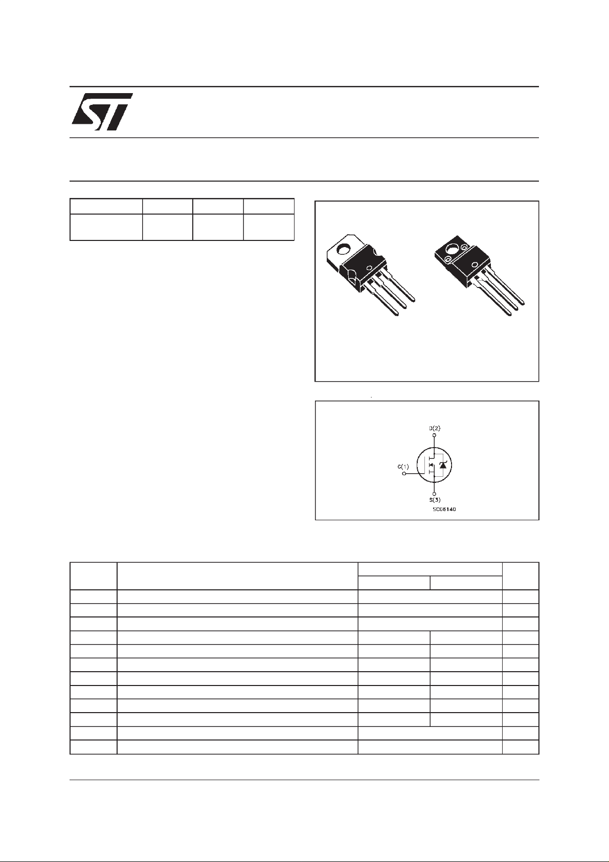
STP5NB60FP
PowerMESH MOSFET
3
2
1
TO-220 TO-220FP
INTERNAL SCHEMATIC DIAGRAM
3
2
1
APPLICATIONS
■ HIGHCURRENT, HIGHSPEED SWITCHING
■ SWITCHMODE POWER SUPPLIES(SMPS)
■ DC-AC CONVERTERS FOR WELDING
EQUIPMENTAND UNINTERRUPTIBLE
POWERSUPPLIESAND MOTORDRIVE
ABSOLUTE MAXIMUM RATINGS
Symbol Parameter Value Unit
ST P5 NB60 STP 5NB 60FP
V
V
V
I
DM
P
dv/ dt(
V
T
(•) Pulse width limited by safe operatingarea (1)ISD≤ 5A, di/dt ≤ 200 A/µs,VDD≤ V
September 1999
Drain-source Voltage ( VGS=0) 600 V
DS
Dra in- gat e Volt a ge (RGS=20kΩ)
DGR
Gate -source V oltage ± 30 V
GS
Dra in Curr en t (c ontinuous) a t Tc=25oC53A
I
D
Dra in Curr en t (c ontinuous) a t Tc= 100oC3.11.9A
I
D
600 V
(•) Dra in Curr en t (p uls ed) 20 20 A
Tot al Dis s ipation at Tc=25oC 100 35 W
tot
Der at ing Fact or 0.8 0.28 W/
) Peak Diode Recov ery voltag e s lop e 4.5 4.5 V/ ns
1
Insulation Withstand Voltage (DC) 2000 V
ISO
St orage Te mpe ra t ure -65 to 150
stg
Max. O perati ng Junction T em p e ra t ure 150
T
j
(BR)DSS
,Tj≤T
JMAX
o
C
o
C
o
C
1/9
Page 2
STP5NB60/FP
THERMAL DATA
R
thj-case
R
thj-amb
R
thc-sink
T
AVALANCHE CHARACTERISTICS
Ther mal Resis t an ce Junc ti on-cas e Max 1.25 3.57
Ther mal Resis t an ce Junc ti on-ambien t M a x
Thermal Resistance Case-sink Typ
Maximum Le ad Tem peratu r e F or Sold er ing Purp ose
l
TO-220 TO220-FP
62.5
0.5
300
o
C/W
o
C/W
o
C/W
o
C
Symbol P ara meter Mi n .
I
AR
E
ELECTRICAL CHARACTERISTICS
Avalanche Curr ent, Repetitive or Not- Re petitiv e
(pulse width l imited by T
Single Pu lse Avalanche Energ y
AS
(starting T
=25oC, ID=IAR,VDD=50V)
j
max)
j
(T
case
=25oC unless otherwisespecified)
Value
Max.
Value
5A
300 mJ
OFF
Symbol Parameter Test Condit ions Min. Typ. Max. Unit
V
(BR)DSS
Drain-sourc e
=250µAVGS=0
I
D
600 V
Break d own Vo lt age
I
DSS
I
GSS
Zero Gate Voltage
Drain Cu rr ent (V
GS
Gat e- b ody Leakage
Current (V
DS
=0)
=0)
=MaxRating
V
DS
V
= Max Rating Tc=125oC
DS
= ± 30 V
V
GS
1
50
± 100 nA
ON(∗)
Symbol Parameter Test Condit ions Min. Typ. Max. Unit
V
GS(th)
R
DS(on)
I
D(on)
Gate Threshold
V
DS=VGSID
Voltage
Static Drain-source O n
VGS=10V ID= 2.5 A 1.8 2.0 Ω
Resistanc e
On St ate Drain Current VDS>I
VGS=10V
= 250 µA
D(on)xRDS(on)max
345V
5.0 A
Unit
µA
A
µ
DYNAMIC
Symbol Parameter Test Condit ions Min. Typ. Max. Unit
g
(∗)Forward
fs
C
iss
C
oss
C
rss
2/9
Tr ansconduc tance
Input Cap aci t ance
Out put Capacit ance
Reverse T ransf er
Capacitance
VDS>I
D(on)xRDS(on)maxID
=2.5A 2.5 4.5 S
VDS=25V f=1MHz VGS=0 680
103
10.5
884
139
14
pF
pF
pF
Page 3
STP5NB60/FP
ELECTRICAL CHARACTERISTICS
(continued)
SWITCHING ON
Symbol Parameter Test Condit ions Min. Typ. Max. Unit
t
d(on)
t
r
Turn-on Time
Rise T im e
VDD= 300 V ID=2.5A
=4.7 Ω VGS=10V
R
G
12
10
17
14
(see t est circuit, fi gure 3)
Q
Q
Q
Total Gate Charge
g
Gat e- Source Charge
gs
Gate-Drain Charge
gd
VDD= 480 V ID=5A VGS=10V 21
7.6
7.5
30 nC
SWITCHING OFF
Symbol Parameter Test Condit ions Min. Typ. Max. Unit
t
r(Voff)
t
t
Off -voltage R ise Time
Fall Time
f
Cross-ov er Ti me
c
VDD= 480 V ID=5A
=4.7 Ω VGS=10V
R
G
(see t est circuit, fi gure 5)
8
7
15
13
12
23
SOURCEDRAINDIODE
Symbol Parameter Test Condit ions Min. Typ. Max. Unit
I
SD
I
SDM
V
SD
t
Q
I
RRM
(∗) Pulsed: Pulse duration = 300 µs, duty cycle 1.5 %
(•) Pulse width limited by safe operatingarea
Source-drain Current
(•)
Source-drain Current
5
20
(pulsed)
(∗) F orwar d O n V oltage ISD=5A VGS=0 1.6 V
Reverse R ecover y
rr
Time
Reverse R ecover y
rr
= 5 A di/dt = 100 A/µs
I
SD
= 100 V Tj=150oC
V
DD
(see t est circuit, fi gure 5)
610
3.6
Charge
Reverse R ecover y
11.7
Current
ns
ns
nC
nC
ns
ns
ns
A
A
ns
µ
A
C
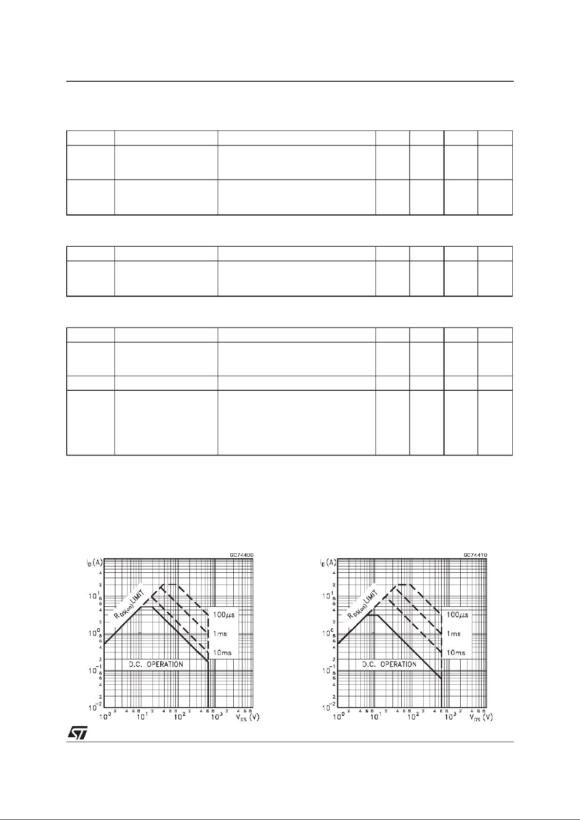
SafeOperating Area for TO-220 SafeOperating Area for TO-220FP
3/9
Page 4

STP5NB60/FP
ThermalImpedancefor TO-220
OutputCharacteristics
ThermalImpedance for TO-220FP
TransferCharacteristics
Transconductance
4/9
Static Drain-sourceOn Resistance
Page 5

STP5NB60/FP
Gate Charge vs Gate-sourceVoltage
Normalized Gate ThresholdVoltage vs
Temperature
CapacitanceVariations
Normalized On Resistance vsTemperature
Source-drainDiode Forward Characteristics
5/9
Page 6

STP5NB60/FP
Fig. 1:
UnclampedInductive Load TestCircuit
Fig. 3: SwitchingTimes TestCircuitsFor
ResistiveLoad
Fig. 2:
UnclampedInductive Waveform
Fig. 4: Gate Chargetest Circuit
Fig. 5:
Test Circuit For InductiveLoad Switching
And Diode Recovery Times
6/9
Page 7

TO-220 MECHANICAL DATA
STP5NB60/FP
DIM.
MIN. TYP. MAX. MIN. TYP. MAX.
A 4.40 4.60 0.173 0.181
C 1.23 1.32 0.048 0.051
D 2.40 2.72 0.094 0.107
D1 1.27 0.050
E 0.49 0.70 0.019 0.027
F 0.61 0.88 0.024 0.034
F1 1.14 1.70 0.044 0.067
F2 1.14 1.70 0.044 0.067
G 4.95 5.15 0.194 0.203
G1 2.4 2.7 0.094 0.106
H2 10.0 10.40 0.393 0.409
L2 16.4 0.645
L4 13.0 14.0 0.511 0.551
L5 2.65 2.95 0.104 0.116
L6 15.25 15.75 0.600 0.620
L7 6.2 6.6 0.244 0.260
L9 3.5 3.93 0.137 0.154
DIA. 3.75 3.85 0.147 0.151
mm inch
E
A
L4
D
F2
F1
G1
H2
G
F
P011C
C
D1
L2
Dia.
L5
L7
L6
L9
7/9
Page 8

STP5NB60/FP
TO-220FP MECHANICAL DATA
DIM.
MIN. TYP. MAX. MIN. TYP. MAX.
A 4.4 4.6 0.173 0.181
B 2.5 2.7 0.098 0.106
D 2.5 2.75 0.098 0.108
E 0.45 0.7 0.017 0.027
F 0.75 1 0.030 0.039
F1 1.15 1.7 0.045 0.067
F2 1.15 1.7 0.045 0.067
G 4.95 5.2 0.195 0.204
G1 2.4 2.7 0.094 0.106
H 10 10.4 0.393 0.409
L2 16 0.630
L3 28.6 30.6 1.126 1.204
L4 9.8 10.6 0.385 0.417
L6 15.9 16.4 0.626 0.645
L7 9 9.3 0.354 0.366
Ø 3 3.2 0.118 0.126
mm inch
E
A
D
B
L3
L6
L7
¯
F1
F
G1
H
G
F2
123
L2
L4
8/9
Page 9

STP5NB60/FP
Information furnishedis believedtobeaccurateand reliable.However, STMicroelectronics assumes no responsibilityforthe consequences
of use of such information nor for any infringement of patents or other rights of third parties which may result from its use. No license is
granted by implication or otherwise under any patent or patent rights of STMicroelectronics. Specificationmentioned in this publication are
subjecttochange without notice. This publicationsupersedesandreplaces all information previouslysupplied. STMicroelectronicsproducts
are not authorized for use as critical components in life support devicesor systemswithout express written approval of STMicroelectronics.
The STlogo is a trademark of STMicroelectronics
1999 STMicroelectronics – Printed in Italy – All Rights Reserved
STMicroelectronics GROUP OF COMPANIES
Australia - Brazil - Canada -China - France - Germany - Italy - Japan - Korea - Malaysia - Malta - Mexico - Morocco - The Netherlands -
Singapore - Spain - Sweden - Switzerland - Taiwan - Thailand - United Kingdom - U.S.A.
http://www.st.com
.
9/9
 Loading...