

Page 1
STP5NB100
N - CHANNEL1000V - 2.4Ω - 5A - TO-220/TO-220FP
TYPE V
ST P5NB100
ST P5NB100FP
ν TYPICALR
ν EXTREMELY HIGH dv/dt CAPABILITY
ν 100% AVALANCHETESTED
ν VERY LOW INTRINSIC CAPACITANCES
ν GATECHARGE MINIMIZED
DS(on)
DSS
1000 V
1000 V
=2.4 Ω
DESCRIPTION
Using the latest high voltage MESH OVERLAY
process, STMicroelectronics has designed an
advanced family of power MOSFETs with
outstanding performances. The new patent
pending strip layout coupled with the Company’s
proprietary edge termination structure, gives the
lowest RDS(on) per area, exceptional avalanche
and dv/dt capabilities and unrivalled gate charge
and switchingcharacteristics.
R
DS(on)
<2.7Ω
<2.7Ω
I
D
5A
5A
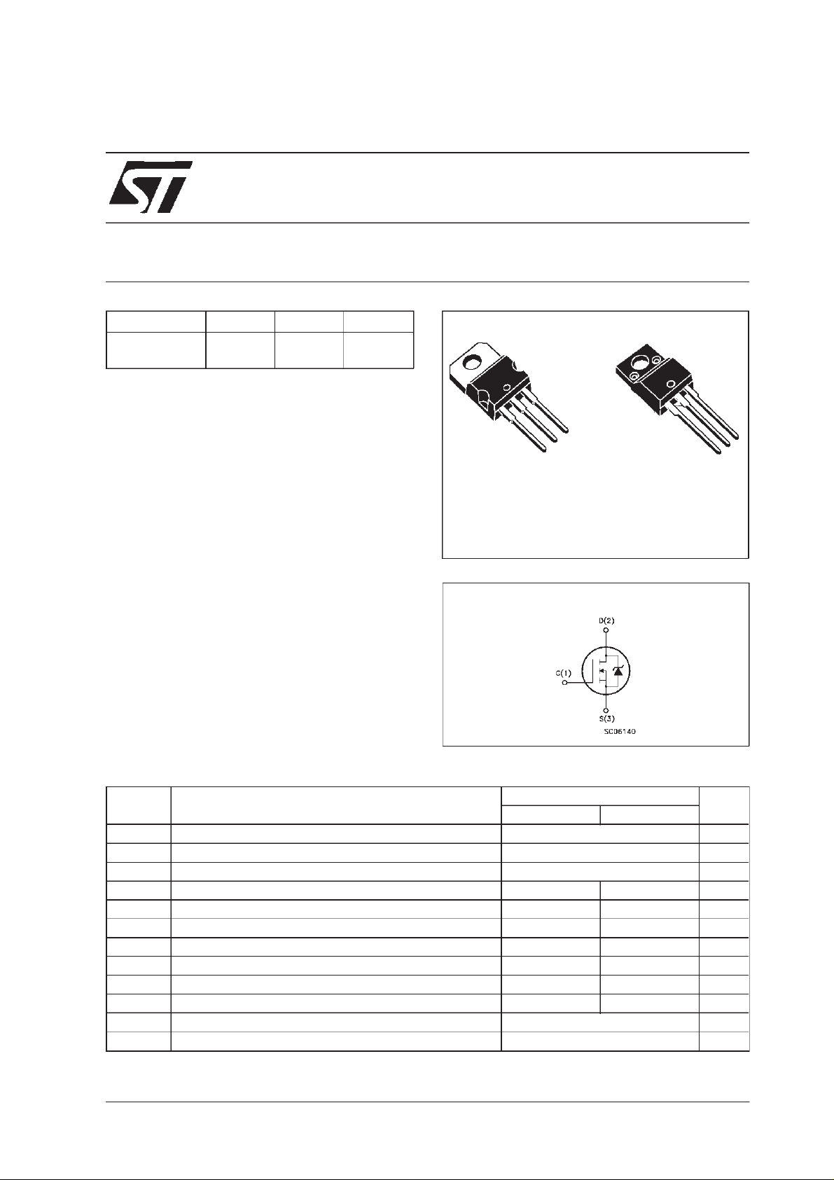
STP5NB100FP
PowerMESH MOSFET
3
2
1
TO-220 TO-220FP
INTERNAL SCHEMATIC DIAGRAM
2
1
3
APPLICATIONS
ν HIGHCURRENT,HIGH SPEED SWITCHING
ν SWITCH MODE POWER SUPPLIES(SMPS)
ν DC-AC CONVERTERSFOR WELDING
EQUIPMENTAND UNINTERRUPTIBLE
POWERSUPPLIESAND MOTOR DRIVE
ABSOLUTE MAXIMUM RATINGS
Symbol Parameter Value Unit
STP5NB100 STP5NB100FP
V
V
V
I
DM
P
dv/ dt(
V
T
(•) Pulse width limited by safe operating area (1)ISD≤ 5 A, di/dt ≤ 200 A/µs, VDD≤ V
(*) Limited only by maximum temperature allowed
February 2000
Drain-source Voltage (VGS=0) 1000 V
DS
Drain- gate Voltage (RGS=20kΩ)
DGR
Gat e-source Voltage ± 30 V
GS
Drain Curren t (cont inu ous) at Tc=25oC 5 5(*) A
I
D
Drain Curren t (cont inu ous) at Tc=100oC 3.1 3.1( *) A
I
D
1000 V
(•) Drain Current (pulsed) 15.2 15.2 A
Tota l Dissipation at Tc=25oC 135 40 W
tot
Derating F actor 1.08 0.32 W/
1) Peak Diode Recov er y vo lt a ge slope 4.5 4.5 V/ ns
Ins u lation Withstand Voltage ( DC) 2000 V
ISO
St orage Temperat ure -65 to 150
stg
Ma x. Operating J unctio n T emperat ure 150
T
j
,Tj≤T
(BR)DSS
JMAX
o
C
o
C
o
C
1/9
Page 2
STP5NB100/STP5NB100FP
THERMAL DATA
TO-220 TO -220F P
R
thj-cas e
R
thj-amb
R
thc-sin k
T
AVALANCHE CHARACTERISTICS
Symb ol Para meter Max Valu e Uni t
I
AR
E
Ther mal Res i s t a nce Jun ct ion-cas e Max 0.93 3.12
Ther mal Res i s t a nce Jun ct ion-ambient Max
Ther mal Res i s t a nce Ca se-s i nk Ty p
Maxim um Lead Temperatur e Fo r Soldering Pur pose
l
Avalanche Cu r rent, Repetitive or Not-Repetitive
(pulse w idth limite d b y T
Single P u ls e Ava lan c he Ener gy
AS
(starting T
=25oC, ID=IAR,VDD=50V)
j
max)
j
62.5
0.5
300
5A
220 mJ
o
C/W
o
C/W
o
C/W
o
C
ELECTRICAL CHARACTERISTICS (T
=25oC unless otherwise specified)
case
OFF
Symbol Parameter Test Cond itions Min. Typ. M ax. Unit
V
(BR) DSS
Drain-source
=250µAVGS=0
I
D
1000 V
Break d own Vo lt a ge
I
DSS
I
GSS
Zero Gate Voltage
Drain Current (V
GS
Gat e- b ody Leak age
Current (V
DS
=0)
=0)
V
= Max Rating
DS
= Max Rating Tc=125oC
V
DS
= ± 30 V
V
GS
1
50
± 100 nA
ON (∗)
Symbol Parameter Test Cond itions Min. Typ. M ax. Unit
V
GS(th)
Gate Threshold
V
DS=VGSID
=250µA
345V
Voltage
R
DS(on)
Static D rain-source On
VGS=10V ID= 2.5 A 2.4 2.7 Ω
Resistance
I
D(on)
On State Dr ain Current VDS>I
D(on)xRDS(on)max
5A
VGS=10V
DYNAMIC
Symbol Parameter Test Cond itions Min. Typ. M ax. Unit
g
(∗)Forward
fs
Tra nsconduct a nc e
C
C
C
Input Capacitance
iss
Out put Capacitanc e
oss
Reverse Trans fer
rss
Capacitance
VDS>I
D(on)xRDS(on)maxID
= 2.5 A 1.5 S
VDS=25V f=1MHz VGS= 0 1500
150
17
µA
µA
pF
pF
pF
2/9
Page 3

STP5NB100/STP5NB100FP
ELECTRICAL CHARACTERISTICS (continued)
SWITCHING ON
Symbol Parameter Test Cond itions Min. Typ. M ax. Unit
t
d(on)
t
r
Turn-on Time
Rise Time
VDD=500V ID=2.5A
=4.7 Ω VGS=10V
R
G
(see test c irc ui t, figure 3)
Q
Q
Q
Total Gate Charge
g
Gate-Source Charge
gs
Gate-Drain Charge
gd
VDD=800V ID=5A VGS=10V 39
SWITCHING OFF
Symbol Parameter Test Cond itions Min. Typ. M ax. Unit
t
r(Voff)
t
Off-voltage Rise Time
Fall Time
t
f
Cross-over T ime
c
VDD=800V ID=5A
=4.7 Ω VGS=10V
R
G
(see test c irc ui t, figure 5)
SOURCEDRAIN DIODE
Symbol Parameter Test Cond itions Min. Typ. M ax. Unit
I
SD
I
SDM
V
SD
t
Q
I
RRM
(∗) Pulsed: Pulse duration = 300 µs, duty cycle 1.5 %
(•) Pulse width limited by safe operatingarea
Source-drain Current
(•)
Source-drain Current
(pulsed)
(∗) Forwar d O n Vol t ag e ISD=5A VGS=0 1.6 V
Reverse Rec overy
rr
Time
Reverse Rec overy
rr
= 5 A di/dt = 100 A/µ s
I
SD
=100V Tj=150oC
V
DD
(see test c irc ui t, figure 5)
Charge
Reverse Rec overy
Current
24
11
51 nC
9.6
19.2
20
22
26
5
20
780
5.5
14
ns
ns
nC
nC
ns
ns
ns
A
A
ns
µC
A
Safe OperatingArea for TO-220 Safe Operating Area for TO-220FP
3/9
Page 4

STP5NB100/STP5NB100FP
Thermal Impedancefor TO-220
OutputCharacteristics
ThermalImpedance forTO-220FP
TransferCharacteristics
Transconductance
4/9
StaticDrain-sourceOn Resistance
Page 5

STP5NB100/STP5NB100FP
Gate Charge vs Gate-sourceVoltage
NormalizedGate Threshold Voltage vs
Temperature
CapacitanceVariations
Normalized On Resistance vs Temperature
Source-drainDiode Forward Characteristics
5/9
Page 6

STP5NB100/STP5NB100FP
Fig. 1: UnclampedInductive Load Test Circuit
Fig. 3: SwitchingTimes Test CircuitsFor
ResistiveLoad
Fig. 2: UnclampedInductiveWaveform
Fig. 4: GateCharge test Circuit
Fig. 5: Test Circuit For InductiveLoad Switching
And DiodeRecovery Times
6/9
Page 7

TO-220 MECHANICAL DATA
STP5NB100/STP5NB100FP
DIM.
MIN. TYP. MAX. MIN. TYP. MAX.
A 4.40 4.60 0.173 0.181
C 1.23 1.32 0.048 0.051
D 2.40 2.72 0.094 0.107
D1 1.27 0.050
E 0.49 0.70 0.019 0.027
F 0.61 0.88 0.024 0.034
F1 1.14 1.70 0.044 0.067
F2 1.14 1.70 0.044 0.067
G 4.95 5.15 0.194 0.203
G1 2.4 2.7 0.094 0.106
H2 10.0 10.40 0.393 0.409
L2 16.4 0.645
L4 13.0 14.0 0.511 0.551
L5 2.65 2.95 0.104 0.116
L6 15.25 15.75 0.600 0.620
L7 6.2 6.6 0.244 0.260
L9 3.5 3.93 0.137 0.154
DIA. 3.75 3.85 0.147 0.151
mm inch
E
A
L4
D
F2
F1
G1
H2
G
F
P011C
C
D1
L2
Dia.
L5
L7
L6
L9
7/9
Page 8

STP5NB100/STP5NB100FP
TO-220FP MECHANICAL DATA
DIM.
MIN. TYP. MAX. MIN. TYP. MAX.
A 4.4 4.6 0.173 0.181
B 2.5 2.7 0.098 0.106
D 2.5 2.75 0.098 0.108
E 0.45 0.7 0.017 0.027
F 0.75 1 0.030 0.039
F1 1.15 1.7 0.045 0.067
F2 1.15 1.7 0.045 0.067
G 4.95 5.2 0.195 0.204
G1 2.4 2.7 0.094 0.106
H 10 10.4 0.393 0.409
L2 16 0.630
L3 28.6 30.6 1.126 1.204
L4 9.8 10.6 0.385 0.417
L6 15.9 16.4 0.626 0.645
L7 9 9.3 0.354 0.366
Ø 3 3.2 0.118 0.126
mm inch
E
A
D
B
L3
L6
L7
¯
F1
F
G1
H
G
F2
123
L2
L4
8/9
Page 9

STP5NB100/STP5NB100FP
Information furnishedis believedto be accurate and reliable.However, STMicroelectronics assumes no responsibilityfor the consequences
of use of such information nor for any infringement of patents or other rights of third parties which may result from its use. No license is
granted by implication or otherwise under any patent or patent rights of STMicroelectronics. Specification mentioned in this publication are
subjectto change without notice.This publication supersedesand replaces all information previously supplied.STMicroelectronicsproducts
are notauthorized for use as critical components in life support devices or systems without express written approval of STMicroelectronics.
The ST logo is a trademark of STMicroelectronics
1999 STMicroelectronics – Printed in Italy – All RightsReserved
STMicroelectronics GROUP OF COMPANIES
Australia - Brazil - China - Finland - France- Germany - Hong Kong - India - Italy - Japan - Malaysia - Malta - Morocco -
Singapore - Spain - Sweden - Switzerland - United Kingdom - U.S.A.
http://www.st.com
.
9/9
 Loading...