

Page 1
STP4NC60
STP4NC60FP
N - CHANNEL 600V- 1.8 Ω - 4.2 A TO-220/TO-220FP
PowerMESH ΙΙ MOSFET
TYPE V
ST P4 NC60
ST P4 NC60FP
n TYPICALR
n EXTREMELYHIGHdv/dt CAPABILITY
n 100% AVALANCHETESTED
n NEWHIGH VOLTAGEBENCHMARK
n GATECHARGE MINIMIZED
DS(on)
DSS
600 V
600 V
=1.8 Ω
DESCRIPTION
The PowerMESH ΙΙ is the evolution of the first
generation of MESH OVERLAY. The layout
refinements introduced greatly improve the
Ron*area figureof meritwhile keeping the device
at the leading edge for what concerns switching
speed,gate chargeand ruggedness.
APPLICATIONS
n HIGHCURRENT,HIGH SPEEDSWITCHING
n SWITHMODE POWER SUPPLIES(SMPS)
n DC-AC CONVERTERSFORWELDING
EQUIPMENTANDUNINTERRUPTIBLE
POWERSUPPLIESAND MOTOR DRIVER
R
DS(on)
<2.2 Ω
<2.2 Ω
I
D
4.2 A
4.2 A
3
2
1
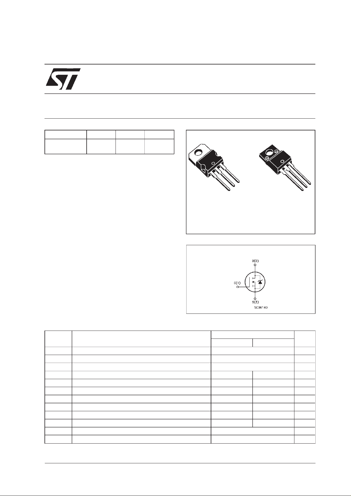
TO-220 T0-220FP
INTERNAL SCHEMATIC DIAGRAM
3
2
1
ABSOLUTE MAXIMUM RATINGS
Symbol Parameter Value Uni t
ST P4NC6 0 ST P4 NC60FP
V
V
V
I
DM
P
dv/dt(
V
T
(•) Pulse width limited by safeoperating area (1)ISD≤ 4.2A, di/dt ≤ 200 A/µs,VDD≤ V
(*) Limited only by maximum temperature allowed
February 2000
Drain-s ource Voltage ( VGS= 0) 600 V
DS
Drain- gat e Volt age (RGS=20kΩ) 600 V
DGR
Gat e- source Voltage ± 30 V
GS
Drain Current (continuous) at Tc=25oC4.24.2(*)A
I
D
Drain Current (continuous) at Tc= 100oC2.62.6(*)A
I
D
(•) Drain Current ( pu ls ed) 16. 8 16.8 A
Tot al Dissipat ion at Tc=25oC 100 35 W
tot
Derat ing Fact or 0.8 0. 28 W/
1) Peak D iode R ecovery voltage s lope 3 3 V/ns
Ins ulat ion Withs tand Volt age (DC) 2000 V
ISO
Sto rage T emperatur e -65 to 150
stg
Max. Oper at in g Junc t ion Temperat ur e 150
T
j
,Tj≤T
(BR)DSS
JMAX
o
C
o
C
o
C
1/9
Page 2
STP4NC60/FP
THERMAL DATA
TO-220 TO-220FP
R
thj-cas e
Rthj- amb
R
thc-sin k
T
AVALANCHE CHARACTERISTICS
Sym b ol Param et er Max V alue Unit
I
AR
E
Therma l Resist ance Junction- case Max 1.25 3.57
Therma l Resist ance Junction- ambient M ax
Therma l Resist ance C as e -s ink Typ
Maxim um Lead T e m pera t ur e For Soldering Purpose
l
Avalanc he Current, Rep et it ive or Not -Repetitive
(pulse widt h limit ed by T
Single Pulse Av alanche Energy
AS
(starting T
=25oC, ID=IAR,VDD=50V)
j
max)
j
62.5
0.5
300
4.2 A
170 mJ
o
C/W
o
C/W
o
C/W
o
C
ELECTRICAL CHARACTERISTICS (T
=25oC unlessotherwisespecified)
case
OFF
Sym b ol Param eter Tes t Condit ions Min. Ty p. Max. Unit
V
(BR) DSS
Drain-so urce
ID= 250 µAVGS= 0 600 V
Break down Voltage
I
DSS
I
GSS
Zero Gate Voltage
Drain Current (V
GS
Gate-body Leakage
Current (V
DS
=0)
=0)
V
=MaxRating
DS
= Max Rating Tc=125oC
V
DS
V
= ± 30 V ± 100 nA
GS
1
50
ON (∗)
Sym b ol Param eter Tes t Condit ions Min. Ty p. Max. Unit
V
GS(th)
R
DS(on)
Gate Threshold Voltage VDS=VGSID=250µA234V
Static Drain-source On
VGS= 10V ID=2A 1.8 2.2 Ω
Resist ance
I
D(on)
On Stat e Drain Current VDS>I
D(on)xRDS(on)max
4.2 A
VGS=10V
DYNAMIC
Sym b ol Param eter Tes t Condit ions Min. Ty p. Max. Unit
g
(∗)Forward
fs
Transconduct ance
Input Capacit ance
iss
Output Capacitance
Reverse Transfer
rss
C
C
oss
C
Capacit ance
VDS>I
D(on)xRDS(on)maxID
=2A 3.7 S
VDS=25V f=1MHz VGS= 0 475
72
10
µA
µA
pF
pF
pF
2/9
Page 3
STP4NC60/FP
ELECTRICAL CHARACTERISTICS (continued)
SWITCHING ON
Sym b ol Param eter Tes t Condit ions Min. Typ. Max . Unit
t
d(on)
t
r
Turn-on T ime
Rise Tim e
VDD=300V ID=2A
=4.7 Ω VGS=10V
R
G
(see test circuit , figure 3)
Q
Q
Q
Total Gate Charge
g
Gate-Sourc e Charge
gs
Gate-Drain Charg e
gd
VDD=480V ID=4.2A VGS= 10 V 16.5
SWITCHING OFF
Sym b ol Param eter Tes t Condit ions Min. Typ. Max . Unit
t
r(Voff)
t
t
Off -voltag e Ri s e T ime
Fall Time
f
Cross -over Tim e
c
VDD=480V ID=4.2A
=4.7 Ω VGS=10V
R
G
(see test circuit , figure 5)
SOURCEDRAIN DIODE
Sym b ol Param eter Tes t Condit ions Min. Typ. Max . Unit
I
SD
I
SDM
V
SD
t
Q
I
RRM
(∗) Pulsed: Pulse duration = 300µs, dutycycle 1.5 %
(•) Pulse width limitedby safe operatingarea
Source-drain Current
(•)
Source-drain Current
(pulsed)
(∗)ForwardOnVoltage ISD=4.2A VGS=0 1.6 V
Revers e R ecover y
rr
Time
Revers e R ecover y
rr
ISD= 4.2 A di/dt = 100 A/µs
=100V Tj= 150oC
V
DD
(see test circuit , figure 5)
Charge
Revers e R ecover y
Current
14
14
23.1 nC
2.5
9
15
19
24
4.2
16.8
600
2.7
9
ns
ns
nC
nC
ns
ns
ns
A
A
ns
µC
A
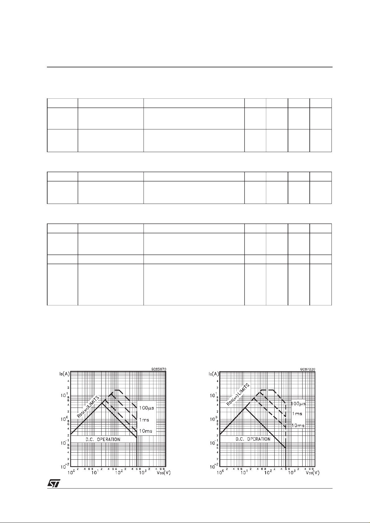
Safe OperatingArea Safe Operating Area for TO-220FP
3/9
Page 4

STP4NC60/FP
ThermalImpedance
OutputCharacteristics
ThermalImpedancefor TO-220FP
TransferCharacteristics
Transconductance
4/9
StaticDrain-sourceOn Resistance
Page 5

STP4NC60/FP
Gate Chargevs Gate-sourceVoltage
NormalizedGate Threshold Voltage vs
Temperature
CapacitanceVariations
Normalized OnResistancevs Temperature
Source-drainDiode Forward Characteristics
5/9
Page 6

STP4NC60/FP
Fig. 1: Unclamped InductiveLoad Test Circuit
Fig. 3: SwitchingTimes TestCircuits For
ResistiveLoad
Fig. 2: UnclampedInductive Waveform
Fig. 4: Gate Chargetest Circuit
Fig. 5: TestCircuitFor InductiveLoad Switching
And DiodeRecovery Times
6/9
Page 7

TO-220 MECHANICAL DATA
STP4NC60/FP
DIM.
MIN. TYP. MAX. MIN. TYP. MAX.
A 4.40 4.60 0.173 0.181
C 1.23 1.32 0.048 0.051
D 2.40 2.72 0.094 0.107
D1 1.27 0.050
E 0.49 0.70 0.019 0.027
F 0.61 0.88 0.024 0.034
F1 1.14 1.70 0.044 0.067
F2 1.14 1.70 0.044 0.067
G 4.95 5.15 0.194 0.203
G1 2.4 2.7 0.094 0.106
H2 10.0 10.40 0.393 0.409
L2 16.4 0.645
L4 13.0 14.0 0.511 0.551
L5 2.65 2.95 0.104 0.116
L6 15.25 15.75 0.600 0.620
L7 6.2 6.6 0.244 0.260
L9 3.5 3.93 0.137 0.154
DIA. 3.75 3.85 0.147 0.151
mm inch
E
A
L4
D
F2
F1
G1
H2
G
F
P011C
C
D1
L2
Dia.
L5
L7
L6
L9
7/9
Page 8

STP4NC60/FP
TO-220FPMECHANICAL DATA
DIM.
MIN. TYP. MAX. MIN. TYP. MAX.
A 4.4 4.6 0.173 0.181
B 2.5 2.7 0.098 0.106
D 2.5 2.75 0.098 0.108
E 0.45 0.7 0.017 0.027
F 0.75 1 0.030 0.039
F1 1.15 1.7 0.045 0.067
F2 1.15 1.7 0.045 0.067
G 4.95 5.2 0.195 0.204
G1 2.4 2.7 0.094 0.106
H 10 10.4 0.393 0.409
L2 16 0.630
L3 28.6 30.6 1.126 1.204
L4 9.8 10.6 0.385 0.417
L6 15.9 16.4 0.626 0.645
L7 9 9.3 0.354 0.366
Ø 3 3.2 0.118 0.126
mm inch
E
A
D
8/9
B
L3
L6
L7
¯
F1
F
G1
H
2
F
G
123
L2
L4
Page 9

STP4NC60/FP
Information furnishedis believed to be accurate and reliable.However, STMicroelectronics assumes no responsibilityfor the consequences
of use of such information nor for any infringementof patents or other rights of third parties which may result from its use. No license is
granted by implication or otherwise underany patent or patent rights of STMicroelectronics. Specification mentioned in this publication are
subjectto change without notice.This publication supersedesand replaces all information previously supplied. STMicroelectronics products
are notauthorized for use as critical components inlife supportdevicesor systems without express written approval of STMicroelectronics.
The ST logo is a trademark of STMicroelectronics
1999 STMicroelectronics – Printed in Italy – All Rights Reserved
STMicroelectronics GROUP OF COMPANIES
Australia - Brazil - China - Finland - France- Germany - Hong Kong - India - Italy - Japan - Malaysia - Malta - Morocco -
Singapore -Spain - Sweden - Switzerland - United Kingdom - U.S.A.
http://www.st.com
.
9/9
 Loading...