

Page 1
STP4NB80
®
N - CHANNEL 800V - 3Ω - 4A - TO-220/TO-220FP
TYPE V
STP4NB80
STP4NB80FP
■ TYPICAL R
■ EXTREMELY HIGH dv/dt CAPABILITY
■ 100% AVALANCHE TESTED
■ VERY LOW INTRINSIC CAPACITANCES
■ GATE CHARGE MINIMIZED
DS(on)
DSS
800 V
800 V
= 3 Ω
DESCRIPTION
Using the latest high voltage MESH OVERLAY
process, STMicroelectronics has designed an
advanced family of power MOSFETs with
outstanding performances. The new patent
pending strip layout coupled with the Company’s
proprietary edge termination structure, gives the
lowest RDS(on) per area, exceptional avalanche
and dv/dt capabilities and unrivalled gate charge
and switching characteristics.
R
DS(on)
3.3 Ω
3.3 Ω
I
4 A
4 A
D
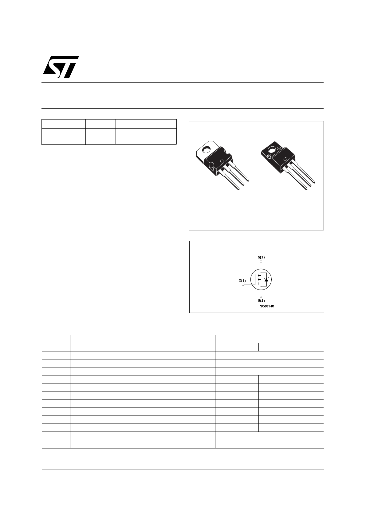
STP4NB80FP
PowerMESH MOSFET
3
2
1
TO-220 TO-220FP
INTERNAL SCHEMAT I C DIAGRAM
3
2
1
APPLICATIONS
■ HIGH CURRENT, HIGH SPEED S WITCHI NG
■ SWITCH MODE PO W E R S UPPLIES (SM PS )
■ DC-AC CONVERT E RS F OR W ELDI NG
EQUIPMENT AND UN INTERRUPTIBLE
POWER SUPPLIES AND MOTOR DRIVE
ABSOLUTE MA XIMU M RAT INGS
Symbol Parameter Value Unit
STP4NB80 STP4NB80FP
V
V
V
I
DM
P
dv/dt(1) Peak Diode Recovery voltage slope 4.5 4.5 V/ns
V
T
(•) Pulse width limited by safe operating area (1) ISD ≤4 A, di/dt ≤ 200 A/µs, VDD ≤ V
(*) Limited only by maximum temperature allowed
September 2001
Drain-source Voltage (VGS = 0) 800 V
DS
Drain- gate Voltage (RGS = 20 kΩ)
DGR
Gate-source Voltage ± 30 V
GS
I
Drain Current (continuous) at Tc = 25 oC 4 4(*) A
D
Drain Current (continuous) at Tc = 100 oC 2.4 2.4(*) A
I
D
800 V
(•) Drain Current (pulsed) 16 16 A
Total Dissipation at Tc = 25 oC 100 35 W
tot
Derating Factor 0.8 0.28 W/
Insulation Withstand Voltage (DC) 2500 V
ISO
Storage Temperature -65 to 150
stg
Max. Operating Junction Temperature 150
T
j
, Tj ≤ T
(BR)DSS
JMAX
o
C
o
C
o
C
1/9
Page 2
STP4NB80/FP
THERMAL DATA
TO-220 TO220-FP
R
thj-case
R
thj-amb
R
thc-sink
T
AVALANCHE CHARACTERISTI CS
Symbol Parameter Max Value Unit
I
AR
E
Thermal Resistance Junction-case Max 1.25 3.6
Thermal Resistance Junction-ambient Max
Thermal Resistance Case-sink Typ
Maximum Lead Temperature For Soldering Purpose
l
Avalanche Current, Repetitive or Not-Repetitive
(pulse width limited by T
Single Pulse Avalanche Energy
AS
(starting T
= 25 oC, ID = IAR, V
j
max)
j
DD
= 50 V)
62.5
0.5
300
4A
230 mJ
o
C/W
o
C/W
o
C/W
o
C
ELECTRICAL CHARACTERISTICS (T
= 25 oC unless otherwise specif ied)
case
OFF
Symbol Parameter Test Conditions Min. Typ. Max. Unit
V
(BR)DSS
Drain-source
I
= 250 µA V
D
GS
= 0
800 V
Breakdown Voltage
I
DSS
I
GSS
Zero Gate Voltage
Drain Current (V
GS
Gate-body Leakage
Current (V
DS
= 0)
= 0)
= Max Rating
V
DS
V
= Max Rating Tc = 125 oC
DS
V
= ± 30 V
GS
1
50
± 100 nA
ON (∗)
Symbol Parameter Test Conditions Min. Typ. Max. Unit
V
GS(th)
R
DS(on)
Gate Threshold Voltage
Static Drain-source On
= VGS ID = 250 µA
V
DS
VGS = 10V ID = 2 A 3 3.3 Ω
345V
Resistance
I
D(on)
On State Drain Current VDS > I
V
= 10 V
GS
D(on)
x R
DS(on)max
4A
DYNAMIC
Symbol Parameter Test Conditions Min. Typ. Max. Unit
g
(∗) Forward
fs
Transconductance
C
C
C
Input Capacitance
iss
Output Capacitance
oss
Reverse Transfer
rss
Capacitance
VDS > I
V
DS
x R
D(on)
DS(on)max
= 25 V f = 1 MHz V
ID = 2 A 1.5 2.9 S
= 0 700
GS
95
920
126
9
12
µA
µA
pF
pF
pF
2/9
Page 3
STP4NB80/F P
ELECTRICAL CHARACTERISTICS (continued)
SWITCHING ON
Symbol Parameter Test Conditions Min. Typ. Max. Unit
t
d(on)
t
Turn-on delay Time
Rise Time
r
V
= 400 V ID = 2 A
DD
RG = 4.7 Ω VGS = 10 V
14
20
8
12
ns
ns
Q
Q
Q
Total Gate Charge
g
Gate-Source Charge
gs
Gate-Drain Charge
gd
V
= 640 V ID = 4 A V
DD
= 10 V 21
GS
7
9
29 nC
SWITCHING OFF
Symbol Parameter Test Conditions Min. Typ. Max. Unit
t
r(Voff)
t
t
Off-voltage Rise Time
Fall Time
f
Cross-over Time
c
V
= 640V ID = 4 A
DD
= 4.7 Ω VGS = 10 V
R
G
12
9
16
17
13
22
SOURCE DRAIN DIODE
Symbol Parameter Test Conditions Min. Typ. Max. Unit
4
16
I
SDM
I
SD
Source-drain Current
(•)
Source-drain Current
(pulsed)
V
(∗) Forward On Voltage ISD =4 A VGS = 0 1.6 V
SD
t
Q
Reverse Recovery
rr
Time
Reverse Recovery
rr
I
= 4 A di/dt = 100 A/µs
SD
V
= 100 V Tj = 150 oC
DD
600
3.3
Charge
I
RRM
Reverse Recovery
11
Current
(∗) Pulsed: Pulse duration = 300 µs, duty cycle 1.5 %
(•) Pulse width limited by safe operating area
nC
nC
ns
ns
ns
A
A
ns
µC
A
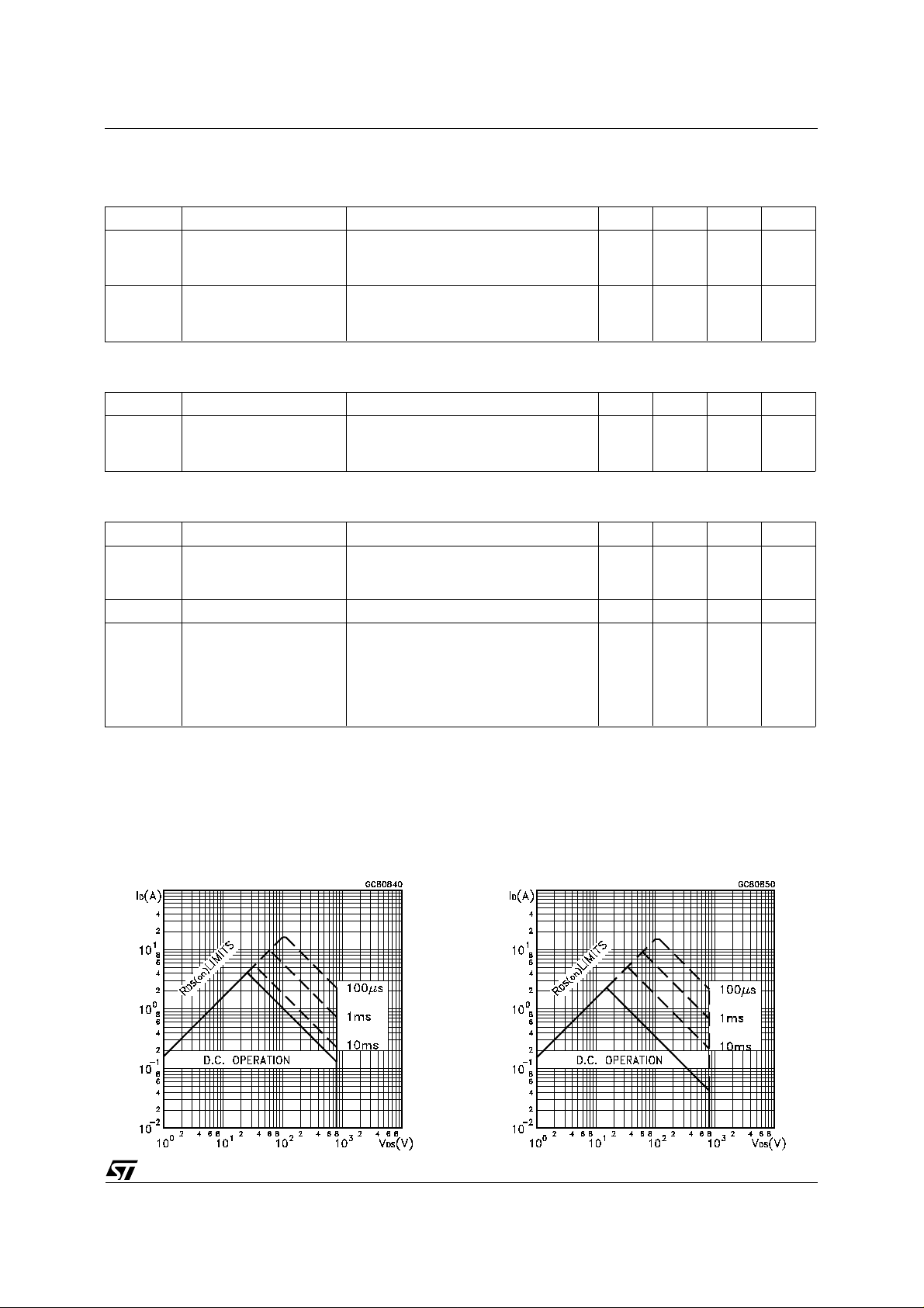
Safe Operating A rea for TO- 220 Safe Operating Ar ea for TO-220FP
3/9
Page 4

STP4NB80/FP
Thermal Impedance for TO- 220
Output Charact eris t ics
Thermal Impedance forTO-220FP
Transfer Charact eris t ics
Transconductanc e
4/9
Static Drain-source O n Resis tance
Page 5

STP4NB80/F P
Gate Charge vs Gate- source Volt ag e
Normalized Gate Thr eshold Volt age vs
Temperature
Capacitance Variations
Normalized On Resistance vs Temper atur e
Source-drain Diode Forward Charact er ist ics
5/9
Page 6

STP4NB80/FP
Fig. 1: Unclamped Inductive Load Test Circuit
Fig. 3: Switc hing Times Tes t Cir cuit s Fo r
Resistive Load
Fig. 2: Unclamped Inductive W av efor m
Fig. 4: Gate Charge tes t Cir cuit
Fig. 5: Test Circuit For Inductiv e Load Sw itching
And Diode Recovery Times
6/9
Page 7

TO-220 MECHANICAL DATA
STP4NB80/FP
DIM.
A 4.40 4.60 0.173 0.181
C 1.23 1.32 0.048 0.052
D 2.40 2.72 0.094 0.107
E 0.49 0.70 0.019 0.027
F 0.61 0.88 0.024 0.034
F1 1.14 1.70 0.044 0.067
F2 1.14 1.70 0.044 0.067
G 4.95 5.15 0.194 0.202
G1 2.40 2.70 0.094 0.106
H2 10.00 10.40 0.394 0.409
L2 16.40 0.645
L4 13.00 14.00 0.511 0.551
L5 2.65 2.95 0.104 0.116
L6 15.25 15.75 0.600 0.620
L7 6.20 6.60 0.244 0.260
L9 3.50 3.93 0.137 0.154
M 2.60 0.102
DIA. 3.75 3.85 0.147 0.151
MIN. TYP. MAX. MIN. TYP. MAX.
mm inch
P011CI
7/9
Page 8

STP4NB80/FP
TO-220FP MECHANICAL DATA
DIM.
MIN. TYP. MAX. MIN. TYP. MAX.
A 4.4 4. 6 0.173 0.181
B 2.5 2. 7 0.098 0.106
D 2.5 2.75 0.098 0.108
E 0.45 0.7 0.017 0.027
F 0.75 1 0.030 0.039
F1 1.15 1.7 0.045 0.067
F2 1.15 1.7 0.045 0.067
G 4.95 5.2 0.195 0.204
G1 2.4 2.7 0.094 0.106
H 10 10.4 0.393 0.409
L2 16 0.630
L3 28.6 30.6 1.126 1.204
L4 9.8 10.6 0.385 0.417
L6 15.9 16.4 0.626 0.645
L7 9 9.3 0.354 0.366
Ø 3 3.2 0.118 0.126
mm inch
A
B
H
E
D
L3
L6
L7
¯
F1
F
G1
G
F2
123
L2
L4
8/9
Page 9

STP4NB80/F P
Information furnished is believed to be accurate and reliable. However, STMicroelectronics assumes no responsibility for the consequences
of use of such inform ation nor for any infringe ment o f patents or other rig hts o f third par ties which ma y resul t from i ts use. N o li cen se is
granted by implicatio n or otherwise under any patent or patent rights of STMicroelectronics. Specification mentioned in this publication are
subject to change without notice. This publication supersedes and replaces all information previously supplied. STMicroelectronics products
are not authorized for use as critical compo nents in life support devices or systems without express written approval of STMicroelectronics.
The ST logo is a trademark of STMicroelectronics
© 2001 STMicroelectro nics – Printed in Italy – All Rights Reserved
STMicroelectronics GROUP OF COMPANIES
Australia - Brazil - China - Finland - France - Germany - Hong Kong - India - Italy - Japan - Malaysia - Malta - Morocco -
Singapore - Spain - Sweden - Switzerland - United Kingdom - U.S.A.
http://www.st.com
9/9
 Loading...