

Page 1
STP4NB50
STP4NB50FP
N - CHANNEL ENHANCEMENT MODE
PowerMESH MOSFET
PRELIMINARY DATA
TYPE V
STP4NB50
STP4NB50FP
■ TYPICALR
■ 100% AVALANCHETESTED
■ VERYLOW INTRINSICCAPACITANCES
■ GATECHARGEMINIMIZED
■ EXTREMELY HIGH dv/dt CAPABILITY
DS(on)
DSS
500 V
500 V
=2.5 Ω
R
DS(on)
<2.8Ω
<2.8Ω
I
D
3.8 A
2.5 A
DESCRIPTION
Using the latest high voltage MESH
OVERLAYprocess, SGS-Thomson has
designed an advanced family of Power
MOSFETs with outstanding performance. The
new patent pending strip layout coupled with the
Company’s proprietary edge termination
structure, gives the lowest RDS(on) per area,
exceptional avalanche and dv/dt capabilitiesand
unrivalled gate charge and switching
characteristics.
APPLICATIONS
■ HIGH CURRENT, HIGH SPEEDSWITCHING
■ SWITCHMODEPOWER SUPPLIES(SMPS)
■ DC-ACCONVERTERS FOR WELDING
EQUIPMENTAND UNINTERRUPTIBLE
P
ABSOLUTE MAXIMUM RATINGS
OWERSUPPLIESAND MOTORDRIVE
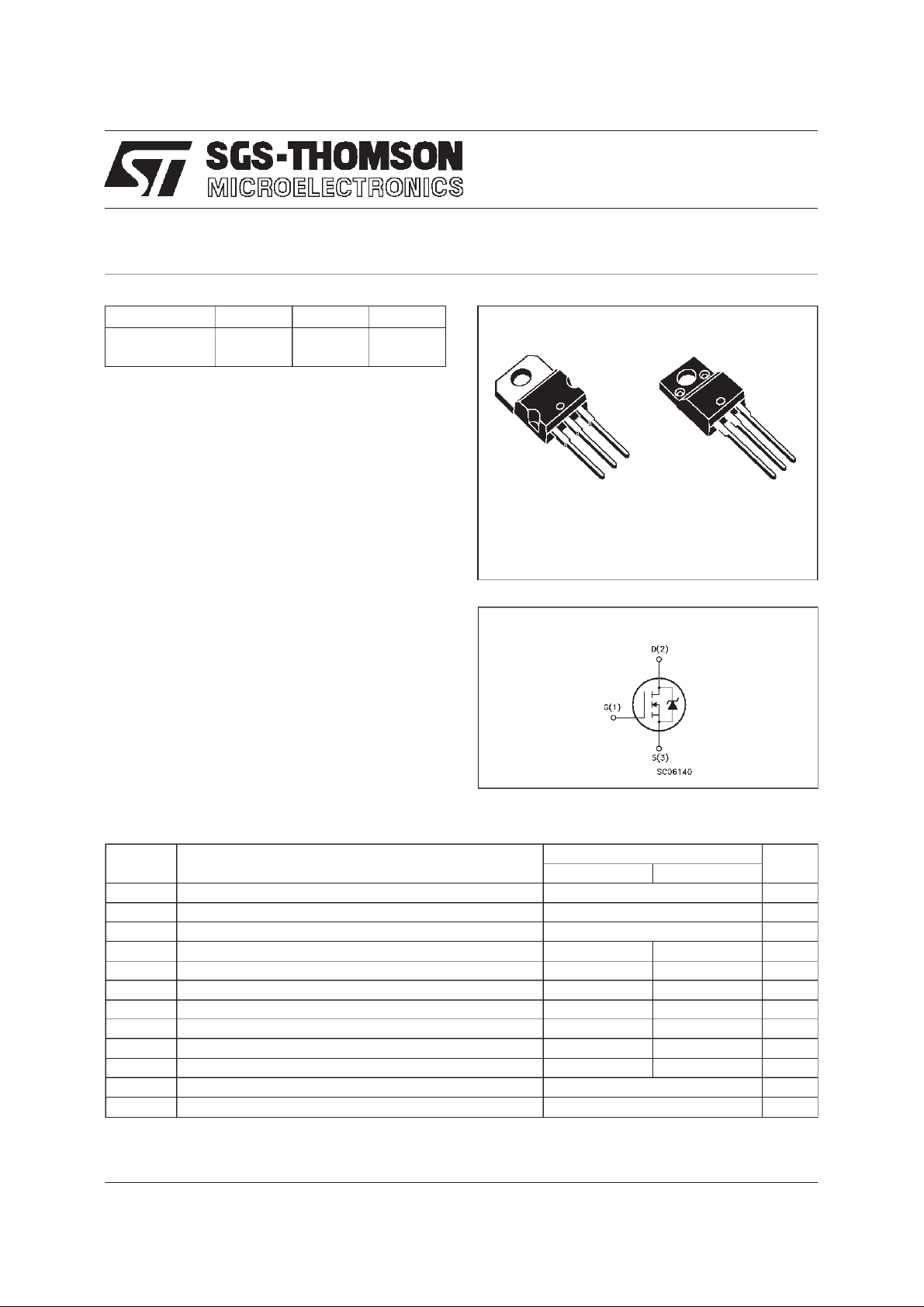
3
2
1
TO-220 TO-220FP
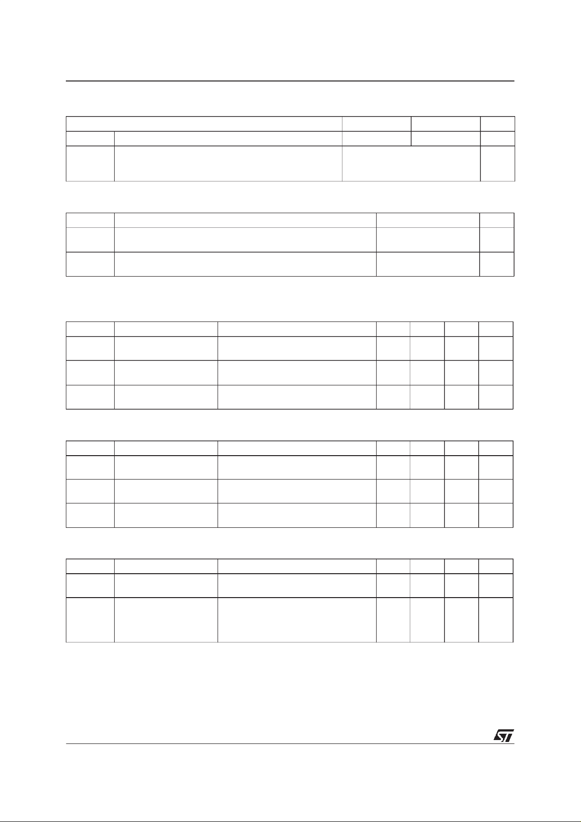
INTERNAL SCHEMATIC DIAGRAM
3
2
1
Symb o l Para meter Value Uni t
ST P4 NB50 S T P4NB50F P
V
V
V
I
DM
P
dv/dt(
V
T
(•) Pulse width limitedby safe operating area (1)ISD≤ 4A, di/dt ≤ 200 A/µs, VDD≤ V
March 1998
This ispreliminary information on a new product now in development or undergoing evaluation. Details are subject to change without notice.
Drain-source V oltage (VGS=0) 500 V
DS
Drain- gate Voltage ( RGS=20kΩ)
DGR
Gat e- sourc e V o lt age ± 30 V
GS
I
Drain Current ( c on t in uous) a t Tc=25oC3.82.5A
D
I
Drain Current ( c on t in uous) a t Tc=100oC2.41.6A
D
500 V
(•) Drain Cur rent (puls ed ) 15.2 15.2 A
Tot al D issipati on at Tc=25oC8035W
tot
Derat in g Factor 0.64 0.28 W/
1) Peak Di ode Re c overy voltage slope 4.5 4.5 V/ns
Ins ulation With s t a nd V oltage (DC) 2000 V
ISO
Sto rage Temperature -65 to 150
stg
T
Max. O peratin g J u nc t io n Temper at u r e 150
j
(BR)DSS
,Tj≤T
JMAX
o
C
o
C
o
C
1/7
Page 2
STP4NB50/FP
THERMAL DATA
TO-220 TO220-FP
R
thj-case
R
thj- amb
R
thc-sin k
T
AVALANCHE CHARACTERISTICS
Symbol Paramete r Max Value Uni t
I
AR
E
Ther mal Resis t an c e J unction-ca se Max 1.56 3.57
Ther mal Resis t an c e J unction-am bie nt Max
Ther mal Resis t an c e C ase-si nk T yp
Maximum Lea d Tem peratu re For Solderi ng P urp os e
l
Avalanch e C ur rent, R ep et it i v e or Not-Re petitiv e
(pulse width limited b y T
Single Pulse Avalanche Energy
AS
(starting T
=25oC, ID=IAR,VDD=50V)
j
max, δ <1%)
j
62.5
0.5
300
3.8 A
220 mJ
o
C/W
o
C/W
o
C/W
o
C
ELECTRICAL CHARACTERISTICS (T
=25oC unlessotherwise specified)
case
OFF
Symbol Parameter Te st Cond ition s Min. Typ. Max. Unit
V
(BR)DSS
Drain-sourc e
=250µAVGS=0
I
D
500 V
Breakdown Voltage
I
DSS
I
GSS
Zer o G at e Voltage
Drain Cur rent (V
GS
Gat e-body Le ak a ge
Current (V
DS
=0)
=0)
=MaxRating
V
DS
V
=MaxRating Tc=125oC
DS
= ± 30 V
V
GS
1
50
± 100 nA
ON (∗)
Symbol Parameter Te st Cond ition s Min. Typ. Max. Unit
V
GS(th )
Gate Threshold
V
DS=VGSID
=250µA
345V
Voltage
R
DS(on)
Stati c D rain-source On
VGS=10V ID= 1.9 A 2.5 2.8 Ω
Resistance
I
D(on)
On St at e Drain Cu rr e nt VDS>I
D(on)xRDS(on)max
3.8 A
VGS=10V
DYNAMIC
Symbol Parameter Te st Cond ition s Min. Typ. Max. Unit
g
(∗)Forward
fs
Tr ansconduc tanc e
C
C
C
Input Ca pac i t ance
iss
Out put Capacitance
oss
Reverse T ransf er
rss
Capa cit an c e
VDS>I
D(on)xRDS(on)maxID
=1.9 A 1.2 2 .3 S
VDS=25V f=1MHz VGS= 0 400
62
7.5
520
84
10
µA
µA
pF
pF
pF
2/7
Page 3
STP4NB50/FP
ELECTRICAL CHARACTERISTICS (continued)
SWITCHINGON
Symbol Parameter Te st Cond ition s Min. Typ. Max. Unit
t
d(on)
Turn-on Tim e
r
Rise T ime
t
VDD=250V ID=1.9A
=4.7 Ω VGS=10V
R
G
11
8
(see test circuit, figure 3)
Q
Q
Q
Total Gate Charge
g
Gat e-Sou rc e Charge
gs
Gate-Drain Charge
gd
VDD=400V ID=3.8A VGS=10V 15
6.5
5
SWITCHINGOFF
Symbol Parameter Te st Cond ition s Min. Typ. Max. Unit
t
r(Voff)
t
t
Of f - voltag e Ris e Tim e
Fall Time
f
Cross-ov er Tim e
c
VDD=400V ID=3.8A
=4.7 Ω VGS=10V
R
G
(see test circuit, figure 5)
8
5
14
SOURCE DRAIN DIODE
Symbol Parameter Te st Cond ition s Min. Typ. Max. Unit
I
SD
I
SDM
V
SD
t
Q
I
RRM
(∗) Pulsed: Pulse duration =300 µs, duty cycle 1.5 %
(•) Pulse width limited by safe operating area
Source-drain Current
(•)
Source-drain Current
(pulsed)
(∗) F orwar d O n Volt age ISD=3.8 A VGS=0 1.6 V
Reverse R ecovery
rr
Time
Reverse R ecovery
rr
=3.8 A di/dt = 100 A/µs
I
SD
=100V Tj=150oC
V
DD
(see test circuit, figure 5)
245
980
Charge
Reverse R ecovery
8
Current
17
12
21 nC
12
9
20
3.8
15.2
ns
ns
nC
nC
ns
ns
ns
A
A
ns
µC
A
3/7
Page 4

STP4NB50/FP
Fig. 1: Unclamped InductiveLoad Test Circuit
Fig. 3: SwitchingTimesTest CircuitsFor
ResistiveLoad
Fig. 2: Unclamped InductiveWaveform
Fig. 4: Gate Charge test Circuit
Fig. 5: Test Circuit For Inductive Load Switching
And Diode RecoveryTimes
4/7
Page 5

TO-220 MECHANICAL DATA
STP4NB50/FP
DIM.
MIN. TYP. MAX. MIN. TYP. MAX.
A 4.40 4.60 0.173 0.181
C 1.23 1.32 0.048 0.051
D 2.40 2.72 0.094 0.107
D1 1.27 0.050
E 0.49 0.70 0.019 0.027
F 0.61 0.88 0.024 0.034
F1 1.14 1.70 0.044 0.067
F2 1.14 1.70 0.044 0.067
G 4.95 5.15 0.194 0.203
G1 2.4 2.7 0.094 0.106
H2 10.0 10.40 0.393 0.409
L2 16.4 0.645
L4 13.0 14.0 0.511 0.551
L5 2.65 2.95 0.104 0.116
L6 15.25 15.75 0.600 0.620
L7 6.2 6.6 0.244 0.260
L9 3.5 3.93 0.137 0.154
DIA. 3.75 3.85 0.147 0.151
mm inch
E
A
L4
D
F2
F1
G1
H2
G
F
C
D1
L2
Dia.
L5
L7
L6
L9
P011C
5/7
Page 6

STP4NB50/FP
TO-220FP MECHANICAL DATA
DIM.
MIN. TYP. MAX. MIN. TYP. MAX.
A 4.4 4.6 0.173 0.181
B 2.5 2.7 0.098 0.106
D 2.5 2.75 0.098 0.108
E 0.45 0.7 0.017 0.027
F 0.75 1 0.030 0.039
F1 1.15 1.7 0.045 0.067
F2 1.15 1.7 0.045 0.067
G 4.95 5.2 0.195 0.204
G1 2.4 2.7 0.094 0.106
H 10 10.4 0.393 0.409
L2 16 0.630
L3 28.6 30.6 1.126 1.204
L4 9.8 10.6 0.385 0.417
L6 15.9 16.4 0.626 0.645
L7 9 9.3 0.354 0.366
Ø 3 3.2 0.118 0.126
mm inch
E
A
D
B
L3
L6
L7
¯
F1
F
G1
H
G
F2
123
L2
L4
6/7
Page 7

STP4NB50/FP
Information furnished is believed to be accurate and reliable. However, SGS-THOMSON Microelectronics assumes no responsability for the
consequences of use of such information nor for any infringement of patents or other rights of third parties which may results from its use. No
license is granted by implication or otherwise under any patent orpatent rights of SGS-THOMSON Microelectronics. Specifications mentioned
in thispublication are subjectto change without notice. This publication supersedes and replaces all information previously supplied.
SGS-THOMSON Microelectronics productsarenot authorizedfor use as critical componentsin life support devices orsystems without express
written approval ofSGS-THOMSON Microelectonics.
1998 SGS-THOMSON Microelectronics - Printed in Italy - All Rights Reserved
Australia - Brazil - Canada - China - France - Germany - Italy - Japan - Korea - Malaysia - Malta - Morocco - The Netherlands -
Singapore - Spain - Sweden - Switzerland - Taiwan - Thailand - United Kingdom - U.S.A
SGS-THOMSON Microelectronics GROUP OF COMPANIES
...
7/7
 Loading...