

Page 1
STP45NF3LL - STP45NF3LLFP
STB45NF3LL
N-CHANNEL 30V - 0.014Ω - 45A TO-220 - TO220FP - D2PAK
STripFET II™ POWER MOSFET
TYPE V
STP45NF3LL
STP45NF3LLFP
STB45NF3LL
■ TYPICAL R
■ OPTIMAL RDS(ON) x Qg TRADE-OFF @ 4 .5V
■ CONDUCTION LOSSES REDUCED
■ SWITCHING LOSSES REDUCED
■ ADDSUFFIX“T4”FORO RDE RING IN TAPE &
DS
DSS
30 V
30 V
30 V
(on) = 0.014Ω @4.5V
R
DS(on)
<0.018Ω
<0.018Ω
<0.018Ω
I
D
45 A
45 A
27 A
REEL
DESCRIPTION
This application specific Power MOSFET is the
third genarat ion of STMicroelectronics unique
“Single Feature Size
™” strip-based process. The
resulting transistor sho ws the best trade-off between on-res istance ang gate charge. When used
as high and low side in buck regulators, it gives the
best perfo rmance in terms of both conduction and
switching losses. This is extremely important for
motherboards where fast switching and high efficiency are of paramount impo rtance.
APPLICATIONS
■ SPECIFICALLY DESIGNED AND OPTIMISED
FOR HIGH EFFICIENCY DC/DC
CONVERTERS
3
2
1
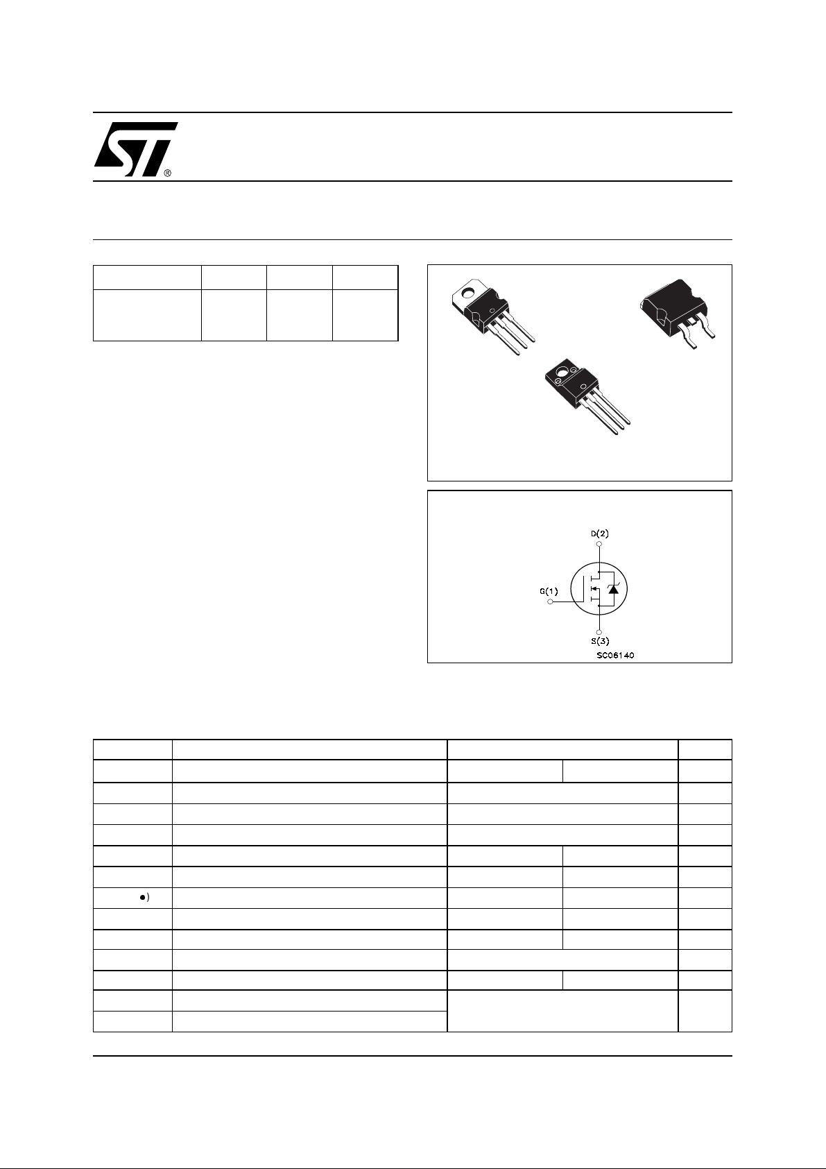
TO-220
1
D2PAK
3
2
TO-220FP
INTERNAL SCHE M ATIC DIAGRAM
3
1
ABSOLUTE MAX IMUM RATINGS
Symbol Parameter Value Unit
2
PAK
45 27 A
32 19 A
70 25 W
I
V
DM
P
V
DGR
V
I
I
TOT
DS
GS
D
D
TO-220/D
Drain-source Voltage (VGS=0)
Drain-gate Voltage (RGS=20kΩ)
Gate- source Voltage ± 16 V
Drain Current (continuous) at TC= 25°C
Drain Current (continuous) at TC= 100°C
()
Drain Current (pulsed) 180 108 A
Total Dissipation at TC= 25°C
Derating Factor 0.46 0.167 W/°C
(1)
E
AS
Single Pulse Avalanche Energy 241 mJ
Viso Insulation Withstand Voltage (DC) -- 2500 V
T
stg
T
j
(●) Pulse width limited by safe operating area
Storage Temperature
Max. Operating Junction Temperature
–55to175 °C
(1) Starting Tj=25°C,ID= 22.5A, VDD=24V
TO-220FP
30 V
30 V
1/11November 2002
Page 2

STP45NF3LL - STB45NF3LL
THERMAL DATA
TO-220
2
D
PAK
Rthj-case Thermal Resistance Junction-case Max 2.14 6 °C/W
Rthj-amb Thermal Resistance Junction-ambient Max 62.5 °C/W
T
l
Maximum Lead Temperature For Soldering Purpose
ELECTRICAL CHARACTE RISTICS (TCASE = 25 °C UNLE S S OTHERWISE SPECIFIED)
OFF
Symbol Parameter Test Conditions Min. Typ. Max. Unit
V
(BR)DSS
Drain-source
ID= 250 µA, VGS= 0 30 V
Breakdown Voltage
I
DSS
I
GSS
Zero Gate Voltage
Drain Current (V
GS
Gate-body Leakage
Current (V
DS
=0)
=0)
V
= Max Rating
DS
= Max Rating, TC= 125 °C
V
DS
V
= ± 16 V ±100 nA
GS
ON (1)
Symbol Parameter Test Conditions Min. Typ. Max. Unit
V
GS(th)
R
DS(on)
Gate Threshold Voltage
Static Drain-source On
Resistance
V
DS=VGS,ID
VGS=10V,ID= 22.5 A
VGS= 4.5V, ID= 22.5 A
= 250µA
1V
TO-220FP
300 °C
1µA
10 µA
0.014 0.018 Ω
0.016 0.020 Ω
DYNAMIC
Symbol Parameter Test Conditions Min. Typ. Max. Unit
(1) Forward Transconductance VDS=15 V,ID=22.5A
g
fs
V
C
iss
C
oss
C
rss
Input Capacitance
Output Capacitance 250 pF
Reverse Transfer
=25V,f=1MHz,VGS=0
DS
Capacitance
20 S
800 pF
60 pF
2/11
Page 3
STP45NF3LL - STB45NF3LL
ELECTRICAL CHARACTE RISTICS (CONTINUED)
SWITCHING ON
Symbol Parameter Test Conditions Min. Typ. Max. Unit
V
t
d(on)
Q
Q
Q
t
r
g
gs
gd
Turn-on Delay Time
Rise Time 100 ns
Total Gate Charge
Gate-Source Charge
Gate-Drain Charge
SWITCHING OFF
Symbol Parameter Test Conditions Min. Typ. Max. Unit
t
d(off)
t
f
Turn-off-Delay Time
Fall Time
SOURCE DRAIN DIODE
Symbol Parameter Test Conditions Min. Typ. Max. Unit
I
SD
I
SDM
VSD(1)
t
rr
Q
rr
I
RRM
Note: 1. Pulsed: Pulse duration = 300 µs, duty cycle 1.5 %.
2. Pulse width limited by safe operating area.
Source-drain Current 45 A
(2)
Source-drain Current (pulsed) 180 A
Forward On Voltage
Reverse Recovery Time
Reverse Recovery Charge
Reverse Recovery Current
=15V,ID= 22.5A
DD
= 4.7Ω VGS=4.5V
R
G
(Resistive Load, see Fig. 3)
=24V,ID= 45A,
V
DD
V
=5V
GS
= 15V, ID= 22.5A,
V
DD
RG=4.7Ω, VGS= 4.5V
(Resistive Load, see Fig. 3)
ISD= 45A, VGS=0
= 45A, di/dt = 100A/µs,
I
SD
VDD=15V,Tj= 150°C
(see test circuit, Figure 5)
17 ns
12.5
17 nC
4.6
5.2
20
21
1.3 V
35
44
2.5
nC
nC
ns
ns
ns
nC
A
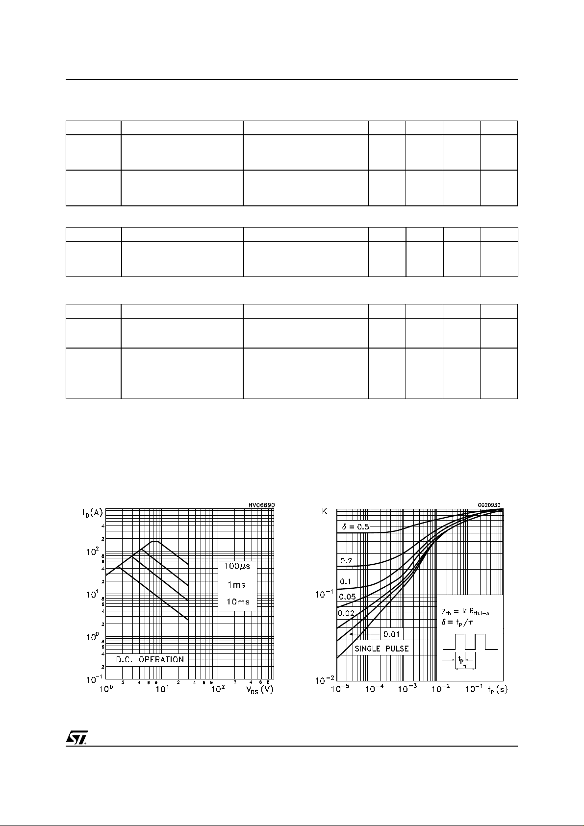
Safe Operating Area for TO-220/D2PAK Thermal Impedance for TO-220/D2PA K
3/11
Page 4

STP45NF3LL - STB45NF3LL
Thermal Impedance for TO-220FPSafe Operating Area for TO-2 20FP
Transfer CharacteristicsOutput Characteristics
Transconductance
4/11
Static Drain-source On Resistance
Page 5

STP45NF3LL - STB45NF3LL
Gate Charge vs Gate-source Voltage
Capacitance Variations
Normalized On Resistance vs TemperatureNormalized Gate T hereshold V ol tage vs Temp.
Source-drain Diode Forward Characteristics Normalized Breakdown Voltage vs Tj
5/11
Page 6

STP45NF3LL - STB45NF3LL
Fig. 2: Unclamped Inductive WaveformFig. 1: Unclamped Inductive Loa d Test Circuit
Fig. 3: Switching Times Test Circuit For
Resistive Load
Fig. 5: Test Circuit For Inductive Load Switching
And Diode Recovery Times
Fig. 4: Gate Charge test Circuit
6/11
Page 7

E
TO-220 MECHANICAL DATA
P011C
STP45NF3LL - STB45NF3LL
DIM.
A 4.40 4.60 0.173 0.181
C 1.23 1.32 0.048 0.051
D 2.40 2.72 0.094 0.107
D1 1.27 0.050
E 0.49 0.70 0.019 0.027
F 0.61 0.88 0.024 0.034
F1 1.14 1.70 0.044 0.067
F2 1.14 1.70 0.044 0.067
G 4.95 5.15 0.194 0.203
G1 2.4 2.7 0.094 0.106
H2 10.0 10.40 0.393 0.409
L2 16.4 0.645
L4 13.0 14.0 0.511 0.551
L5 2.65 2.95 0.104 0.116
L6 15.25 15.75 0.600 0.620
L7 6.2 6.6 0.244 0.260
L9 3.5 3.93 0.137 0.154
DIA. 3.75 3.85 0.147 0.151
MIN. TYP. MAX. MIN. TYP. MAX.
mm inch
A
C
D
L5
Dia.
L7
D1
L6
L2
L9
F1
G1
F
H2
G
F2
L4
7/11
Page 8

STP45NF3LL - STB45NF3LL
TO-220FP MECHANICAL DAT A
DIM.
MIN. TYP. MAX. MIN. TYP. MAX.
A 4.4 4.6 0.173 0.181
B 2.5 2.7 0.098 0.106
D 2.5 2.75 0.098 0.108
E 0.45 0.7 0.017 0.027
F 0.75 1 0.030 0.039
F1 1.15 1.7 0.045 0.067
F2 1.15 1.7 0.045 0.067
G 4.95 5.2 0.195 0.204
G1 2.4 2.7 0.094 0.106
H 10 10.4 0.393 0.409
L2 16 0.630
L3 28.6 30.6 1.126 1.204
L4 9.8 10.6 0.385 0.417
L6 15.9 16.4 0.626 0.645
L7 9 9.3 0.354 0.366
Ø 3 3.2 0.118 0.126
mm inch
E
A
D
8/11
B
L3
L6
L7
¯
F1
F
G1
H
G
F2
123
L2
L4
Page 9

D2PAK MECHANICAL DATA
STP45NF3LL - STB45NF3LL
DIM.
MIN. TYP MAX. MIN. TYP. MAX.
A 4.4 4.6 0.173 0.181
A1 2.49 2.69 0.098 0.106
A2 0.03 0.23 0.001 0.009
B 0.7 0.93 0.027 0.036
B2 1.14 1.7 0.044 0.067
C 0.45 0.6 0.017 0.023
C2 1.23 1.36 0.048 0.053
D 8.95 9.35 0.352 0.368
D1 8 0.315
E 10 10.4 0.393
E1 8.5 0.334
G 4.88 5.28 0.192 0.208
L 15 15.85 0.590 0.625
L2 1.27 1.4 0.050 0.055
L3 1.4 1.75 0.055 0.068
mm. inch
M 2.4 3.2 0.094 0.126
R 0.4 0.015
V2 0º 8º
3
9/11
1
Page 10

STP45NF3LL - STB45NF3LL
D2PAK FOOTPRINT
TAPE AND REEL SHIPMENT (suffix ”T4”)*
TUBE SHIPMENT (no suffix)*
REEL MECHANICAL DATA
DIM.
A 330 12.992
B 1.5 0.059
C 12.8 13.2 0.504 0.520
D 20.2 0795
G 24.4 26.4 0.960 1.039
N 100 3.937
T 30.4 1.197
mm inch
MIN. MAX. MIN. MAX.
TAPE MECHANICAL DATA
DIM.
A0 10.5 10.7 0.413 0.421
B0 15.7 15.9 0.618 0.626
D 1.5 1.6 0.059 0.063
D1 1.59 1.61 0.062 0.063
E 1.65 1.85 0.065 0.073
F 11.4 11.6 0.449 0.456
K0 4.8 5.0 0.189 0.197
P0 3.9 4.1 0.153 0.161
P1 11.9 12.1 0.468 0.476
P2 1.9 2.1 0.075 0.082
R 50 1.574
T 0.25 0.35 0.0098 0.0137
W 23.7 24.3 0.933 0.956
* o n sales type
10/11
mm inch
MIN. MAX. MIN. MAX.
BASE QTY BULK QTY
1000 1000
Page 11

STP45NF3LL - STB45NF3LL
Information furnished is believed to be accurate and reliable. However, STMicroelectronics assumes no responsibilit y for t he
consequences of use of su ch in formation nor for any in fringement of patents or other rights of third parties w hich may result from
its use. No license is granted by implication or otherwise under any patent or patent rights of STMicroelectronics. Specifications
mentioned in this publication are subject to change without notice. This publication supersedes and replaces all information
previously suppli ed. STMi croelect ronics pr oducts are not author ized for use as cr itical component s in li fe suppo rt devi ces or
systems without express written approval of STMicroelectronics.
Australia - Brazil - Canada - China - Finland - France - Germany - Hong Kong - India - Israel - Italy - Japan - Malaysia - Malta - Morocco
© The ST logo is a registered trademark of STMicroelectronics
© 2002 STMicroelectronics - Printed in Italy - All Rights Reserved
Singapore - Spain - Sweden - Switzerland - United Kingdom - United States.
STMicroelectronics GROUP OF COMPANIES
© http://www.st.com
11/11
 Loading...