

Page 1
STP45N10
®
N - CHANNEL 100V - 0.027Ω - 4 5A - TO-220/TO-22 0FI
TYPE V
STP45N10
STP45N10FI
■ TYPICAL R
■ AVALANCHE RUGGED TECHNOLOGY
■ 100% AVALANCHE TESTED
■ REPETITIVE AVA LANCHE DATA AT 100
■ LOW GATE CHARGE
■ HIGH CURRENT CAPABILITY
o
■ 175
■ APPL ICATIO N ORIEN TED
C OPERATING TEMPERATURE
DS(on)
DSS
100 V
100 V
= 0.027 Ω
CHARACTERIZATION
APPLICATIONS
■ HIGH CURRENT, HIGH SPE ED SWI TCHING
■ SOLENOID AND RELAY DRIV ERS
■ DC-DC & DC-AC CONVE RTE RS
■ AUTOMO T IVE ENV I RONME NT (INJ ECT I ON,
ABS, AIR-BAG, LAMP DRIVERS. Etc.)
R
DS(on)
< 0.035 Ω
< 0.035 Ω
I
D
45 A
24 A
o
C
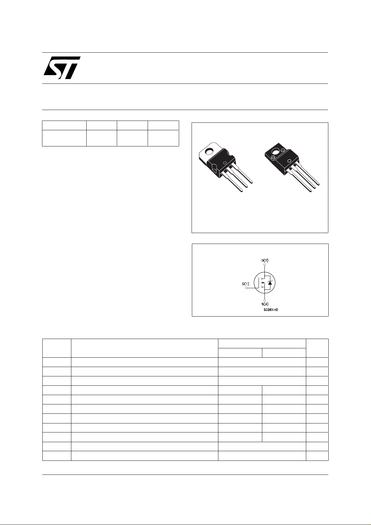
STP45N10FI
POWER MOS TRANSISTOR
3
2
1
TO-220 ISOWATT220
INTER NAL SCH E M ATI C DIAG RA M
3
2
1
ABSOLUTE MAXIMUM RATINGS
Symbol Parameter Value Unit
STP45N10 STP45N10FI
V
V
V
I
DM
P
V
T
June 1998
Drain-source Voltage (VGS = 0) 100 V
DS
Drain- gate Voltage (RGS = 20 kΩ)
DGR
Gate-source Voltage ± 25 V
GS
I
Drain Current (continuous) at Tc = 25 oC4524A
D
I
Drain Current (continuous) at Tc = 100 oC3217A
D
100 V
(•) Drain Current (pulsed) 180 180 A
Total Dissipation at Tc = 25 oC15045W
tot
Derating Factor 1 0.3 W/oC
Insulation Withstand Voltage (DC) 2 000 V
ISO
Storage Temperature -65 to 175
stg
T
Max. Operating Junction Temperature 175
j
o
o
C
C
1/10
Page 2
STP45N10/FI
THERMAL DATA
TO220 ISOWATT220
R
thj-case
R
thj-amb
R
thc-sink
T
AVALANCHE CHARACTERI S TICS
Symbol Parameter Max Value Unit
I
AR
E
Thermal Resistance Junction-case Max 1 3.33
Thermal Resistance Junction-ambient Max
Thermal Resistance Case-sink Typ
Maximum Lead Temperature For Soldering Purpose
l
Avalanche Current, Repetitive or Not-Repetitive
(pulse width limited by T
Single Pulse Avalanche Energy
AS
(starting T
= 25 oC, ID = IAR, V
j
ma x, δ < 1%)
j
= 25 V)
DD
62.5
0.5
300
45 A
400 mJ
o
C/W
o
C/W
o
C/W
o
C
ELECTRICAL CHARACTERISTICS (T
= 25 oC unless otherwise specified)
case
OFF
Symbol Parameter Test Conditions Min. Typ. Max. Unit
V
(BR)DSS
Drain-source
I
= 250 µA V
D
GS
= 0
100 V
Breakdown Voltage
I
DSS
I
GSS
Zero Gate Voltage
Drain Current (V
GS
= 0)
Gate-Source Leakage
Current (V
DS
= 0)
= Max Rating
V
DS
V
= Max Rating x 0.8
DS
V
= Max Rating x 0.8 Tc = 125 oC
DS
V
= ± 20 V
GS
10
1
50
± 100 mA
ON (∗)
Symbol Parameter Test Conditions Min. Typ. Max. Unit
V
GS(th)
Gate Threshold
V
= VGS ID = 250 µA
DS
234V
Voltage
R
DS(on)
I
D(on)
Static Drain-source On
Resistance
VGS = 10 V ID = 22.5 A
V
= 10 V ID = 22.5 A Tc = 100oC
GS
On State Drain Current VDS > I
V
= 10 V
GS
D(on)
x R
DS(on)max
0.027 0.035
0.07
45 A
DYNAMIC
Symbol Parameter Test Conditions Min. Typ. Max. Unit
gfs (∗) Forward
Transconductance
C
C
C
Input Capacitance
iss
Output Capacitance
oss
Reverse Transfer
rss
Capacitance
VDS > I
V
DS
x R
D(on)
DS(on)max
= 25 V f = 1 MHz V
ID = 22.5 A 20 40 S
= 0 4100
GS
600
150
5200
800
220
µA
µA
Ω
Ω
pF
pF
pF
2/10
Page 3
STP45N10/FI
ELECTRICAL CHARACTERISTICS (continued)
SWITCHING O N
Symbol Parameter Test Conditions Min. Typ. Max. Unit
t
d(on)
t
(di/dt)
Q
Q
Q
SWITCHING O F F
Symbol Parameter Test Conditions Min. Typ. Max. Unit
t
r(Voff)
t
SOURCE DRAIN DIO DE
Turn-on Time
Rise Time
r
Turn-on Current Slope V
on
Total Gate Charge
g
Gate-Source Charge
gs
Gate-Drain Charge
gd
Off-voltage Rise Time
Fall Time
t
f
Cross-over Time
c
V
= 50 V ID = 22.5
DD
A
R
= 4.7 Ω VGS = 10 V
G
= 80 V ID = 45 A
DD
= 47 Ω VGS = 10 V
R
G
V
= 80 V ID =45 A V
DD
V
= 80 V ID = 45 A
DD
= 4.7 Ω VGS = 10 V
R
G
GS
25
75
400 A/µs
= 10 V 120
20
50
30
35
65
35
105
170 nC
45
50
95
ns
ns
nC
nC
ns
ns
ns
Symbol Parameter Test Conditions Min. Typ. Max. Unit
45
180
I
SDM
I
SD
Source-drain Current
(•)
Source-drain Current
(pulsed)
V
(∗) Forward On Voltage ISD = 45 A VGS = 0 1.5 V
SD
t
Q
Reverse Recovery
rr
Time
Reverse Recovery
rr
I
= 45 A di/dt = 100 A/µs
SD
V
= 30 V Tj = 150 oC
DD
200
0.14
Charge
I
RRM
Reverse Recovery
14
Current
(∗) Pulsed: Pulse duration = 300 µs, duty cycle 1.5 %
(•) Pulse width limited by safe operating area
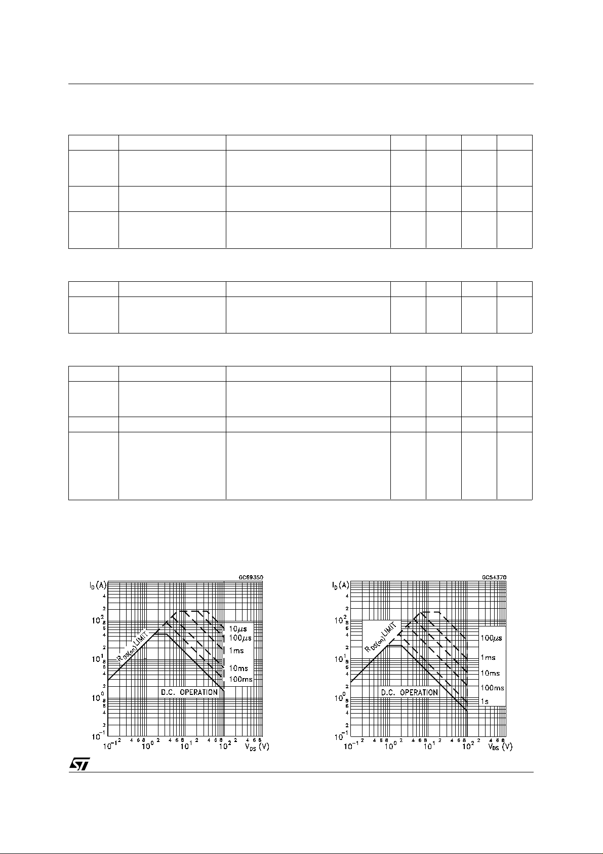
Safe Operating Area for TO-220 Safe Operating Are a for ISOWAT T220
A
A
ns
µC
A
3/10
Page 4

STP45N10/FI
Thermal Impedance for TO-2 20
Derating Curve for TO-220
Thermal Impedance for ISOWATT220
Derating Curve for ISO WA TT 22 0
Output Characteris tics
4/10
Transfer Characteris tic s
Page 5

STP45N10/FI
Transconductance
Gate Charge vs Gate-source Voltage
Static Drain-source On Resist a nce
Capacitance Variations
Normalized Gate Threshold Voltage vs
Temperature
Normalized On Resistance vs Temperature
5/10
Page 6

STP45N10/FI
Turn-on Current Slope
Cross-over Time
Turn-off Drain-source Voltage Slope
Switching Safe Operating Area
Accidental Overload Ar ea
6/10
Source-drain Diode Forward Characteris tics
Page 7

STP45N10/FI
Fig. 1: Unclamped Inductive Load Tes t Circuit
Fig. 3: Switching Times T est Circuits For
Resistive Load
Fig . 2 : Unclamped Inductive Waveform
Fig. 4: Gate Charge test Circuit
Fig. 5: Test Circuit For Inductive Load Switching
And Diode Recovery Times
7/10
Page 8

E
STP45N10/FI
TO-220 MECHANICAL DATA
DIM.
MIN. TYP. MAX. MIN. TYP. MAX.
A 4.40 4.60 0.173 0.181
C 1.23 1.32 0.048 0.051
D 2.40 2.72 0.094 0.107
D1 1.27 0.050
E 0.49 0.70 0.019 0.027
F 0.61 0.88 0.024 0.034
F1 1.14 1.70 0.044 0.067
F2 1.14 1.70 0.044 0.067
G 4.95 5.15 0.194 0.203
G1 2.4 2.7 0.094 0.106
H2 10.0 10.40 0.393 0.409
L2 16.4 0.645
L4 13.0 14.0 0.511 0.551
L5 2.65 2.95 0.104 0.116
L6 15.25 15.75 0.600 0.620
L7 6.2 6.6 0.244 0.260
L9 3.5 3.93 0.137 0.154
DIA. 3.75 3.85 0.147 0.151
mm inch
8/10
A
C
D
D1
L2
F1
L5
Dia.
G1
F
F2
L9
G
H2
L7
L6
L4
P011C
Page 9

ISOWATT220 MECHANICAL DATA
STP45N10/FI
DIM.
MIN. TYP. MAX. MIN. TYP. MAX.
A 4.4 4.6 0.173 0.181
B 2.5 2.7 0.098 0.106
D 2.5 2.75 0.098 0.108
E 0.4 0.7 0.015 0.027
F 0.75 1 0.030 0.039
F1 1.15 1.7 0.045 0.067
F2 1.15 1.7 0.045 0.067
G 4.95 5.2 0.195 0.204
G1 2.4 2.7 0.094 0.106
H 10 10.4 0.393 0.409
L2 16 0.630
L3 28.6 30.6 1.126 1.204
L4 9.8 10.6 0.385 0.417
L6 15.9 16.4 0.626 0.645
L7 9 9.3 0.354 0.366
Ø 3 3.2 0.118 0.126
mm inch
A
B
H
E
D
L3
L6
L7
¯
F1
F
G1
G
F2
123
L2
L4
P011G
9/10
Page 10

STP45N10/FI
Information furnished is believed to be accurate and reliable. However, STMicroelectronics assumes no responsibility for the consequences
of use of such inform ation nor for any infringe ment o f patents or other rig hts o f third par ties which ma y resul t from i ts use. N o li cen se is
granted by implicatio n or otherwise under any patent or patent rights of STMicroelectronics. Specification mentioned in this publication are
subject to change without notice. This publication supersedes and replaces all information previously supplied. STMicroelectronics products
are not authorized for use as critical compo nents in life support devices or systems without express written approval of STMicroelectronics.
The ST logo is a trademark of STMicroelectronics
© 1998 STMicroelectro nics – Printed in Italy – All Rights Reserved
STMicroelectronics GROUP OF COMPANIES
Australia - Brazil - Canada - China - France - Germany - Italy - Japan - Korea - Malaysia - Malta - Morocco - The Netherlands -
Singapore - Spain - Sweden - Switzerland - Taiwan - Thailand - United Kingdom - U.S.A.
.
10/10
 Loading...