

Page 1
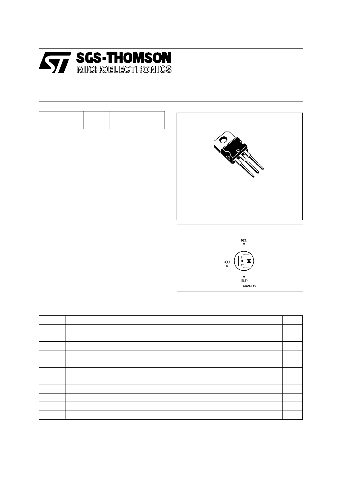
STP40NE03L-20
N - CHANNEL ENHANCEMENT MODE
” SINGLE FEATURE SIZE” POWER MOSFET
TYPE V
DSS
R
DS(on)
I
D
STP40NE03L-20 30 V <0.020 Ω 40 A
■ TYPICALR
■ EXCEPTIONAL dv/dt CAPABILITY
■ LOW GATE CHARGE A 100
■ APPLICATIONORIENTED
DS(on)
= 0.014Ω
o
C
CHARACTERIZATION
DESCRIPTION
This Power MOSFETis the latestdevelopment of
SGS-THOMSON unique ”Single Feature Size”
strip-based process. The resulting transistor
shows extremely high packingdensity for low onresistance, rugged avalanche characteristics and
less critical alignment steps therefore a remarkable manufacturingreproducibility.
APPLICATIONS
■ HIGH CURRENT, HIGHSPEEDSWITCHING
■ SOLENOIDANDRELAY DRIVERS
■ MOTORCONTROL, AUDIOAMPLIFIERS
■ DC-DC& DC-AC CONVERTERSIN HIGH
PERFORMANCEVRMs
■ AUTOMOTIVE ENVIRONMENT(INJECTION,
ABS, AIR-BAG, LAMPDRIVERS,Etc.)
3
2
1
TO-220
INTERNAL SCHEMATIC DIAGRAM
ABSOLUTE MAXIMUM RATINGS
Symbol Parameter Value Unit
V
V
V
I
DM
P
dv/ dt(
T
(•) Pulse width limited by safe operating area (1)ISD≤ 40 A,di/dt ≤ 300 A/µs, VDD≤ V
October 1997
Drain-sourc e Vol t age (VGS=0) 30 V
DS
Drain- gate Vo lt age (RGS=20kΩ)
DGR
Gate- source Voltage ± 15 V
GS
I
Drain Cur rent (con tinuous ) at Tc=25oC40A
D
I
Drain Cur rent (con tinuous ) at Tc=100oC28A
D
30 V
(•) Drain Current (pulsed) 160 A
Total Dissipation at Tc=25oC80W
tot
Derating Fac tor 0.53 W/
1) Pe ak Diode Recov ery voltag e slope 7 V/ns
St orage Te m peratu re -65 to 175
stg
T
Max. Operat ing Junction Temperat ure 175
j
(BR)DSS,Tj≤TJMAX
o
C
o
C
o
C
1/8
Page 2
STP40NE03L-20
THERMAL DATA
R
thj-case
R
thj- amb
R
thc-sin k
T
AVALANCHE CHARACTERISTICS
Symbol Para met e r Max Valu e Uni t
I
AR
E
Ther mal Resist ance Junctio n- ca s e Max
Ther mal Resist ance Junctio n- ambient Max
Ther mal Resist ance Case-si nk Ty p
Maximum Lead T emperat ure For Soldering Purpos e
l
Avalanche Curr e nt , R epetitive o r Not -Re petitiv e
(pulse width limited b y T
Single Pulse Avalanche Energy
AS
(starting T
=25oC, ID=IAR,VDD=15V)
j
max, δ <1%)
j
1.88
62.5
0.5
300
40 A
200 mJ
o
C/W
o
C/W
o
C/W
o
C
ELECTRICAL CHARACTERISTICS (T
=25oC unlessotherwise specified)
case
OFF
Symbol Parameter Test Cond itions Min. Typ. Max. Unit
V
(BR)DSS
Drain-sourc e
=250µAVGS=0
I
D
30 V
Breakdown Voltage
I
I
DSS
GSS
Zer o G at e Volt age
Drain Cur rent (V
GS
Gat e-body Le ak a ge
Current (V
DS
=0)
=0)
=MaxRating
V
DS
V
=MaxRating Tc=125
DS
o
C
= ± 15 V
V
GS
1
10
± 100 nA
ON (∗)
Symbol Parameter Test Cond itions Min. Typ. Max. Unit
V
GS(th )
Gate Threshold
V
DS=VGSID
=250µA
11.82.5V
Voltage
R
DS(on)
I
D(on)
Stati c D rain-source On
Resistance
VGS=10V ID=20A
=5V ID=20A
V
GS
On St at e Dra in Cur rent VDS>I
D(on)xRDS(on)max
0.014 0. 0 2
0.023ΩΩ
40 A
VGS=10V
DYNAMIC
Symbol Parameter Test Cond itions Min. Typ. Max. Unit
g
(∗)Forward
fs
Tr ansconduc tanc e
C
C
C
Input Capacit ance
iss
Out put C apacit ance
oss
Reverse T ransf er
rss
Capa cit an c e
VDS>I
D(on)xRDS(on)maxID
=20A 15 20 S
VDS=25V f=1MHz VGS= 0 1850
450
160
2400
590
210
µA
µA
pF
pF
pF
2/8
Page 3
STP40NE03L-20
ELECTRICAL CHARACTERISTICS (continued)
SWITCHINGON
Symbol Parameter Test Cond itions Min. Typ. Max. Unit
t
d(on)
Q
Q
Q
Turn-on Tim e
Rise T ime
t
r
Total Gate Charge
g
Gat e-Sou rc e Charge
gs
Gate-Drain Charge
gd
VDD=15V ID=20A
=4.7 Ω VGS=5V
R
G
VDD=24V ID=40A VGS=5V 29
SWITCHINGOFF
Symbol Parameter Test Cond itions Min. Typ. Max. Unit
t
r(Voff)
t
Of f - voltag e Ris e Tim e
t
Fall Time
f
Cross-ov er Tim e
c
VDD=24V ID=40A
=4.7 Ω VGS=5V
R
G
SOURCE DRAIN DIODE
Symbol Parameter Test Cond itions Min. Typ. Max. Unit
I
SD
I
SDM
V
SD
t
Q
I
RRM
(∗) Pulsed: Pulse duration =300 µs, duty cycle1.5 %
(•) Pulse width limited by safe operating area
Source-drain Current
(•)
Source-drain Current
(pulsed)
(∗) Forwar d O n Volt age ISD=40A VGS=0 1.5 V
Reverse R ecovery
rr
Time
Reverse R ecovery
rr
= 40 A di/dt = 100 A/µs
I
SD
=20V Tj=150oC
V
DD
Charge
Reverse R ecovery
Current
25
16033210
38 nC
12
14
25
120
155
33
160
210
40
160
50
0.9
3.5
ns
ns
nC
nC
ns
ns
ns
A
A
ns
µC
A
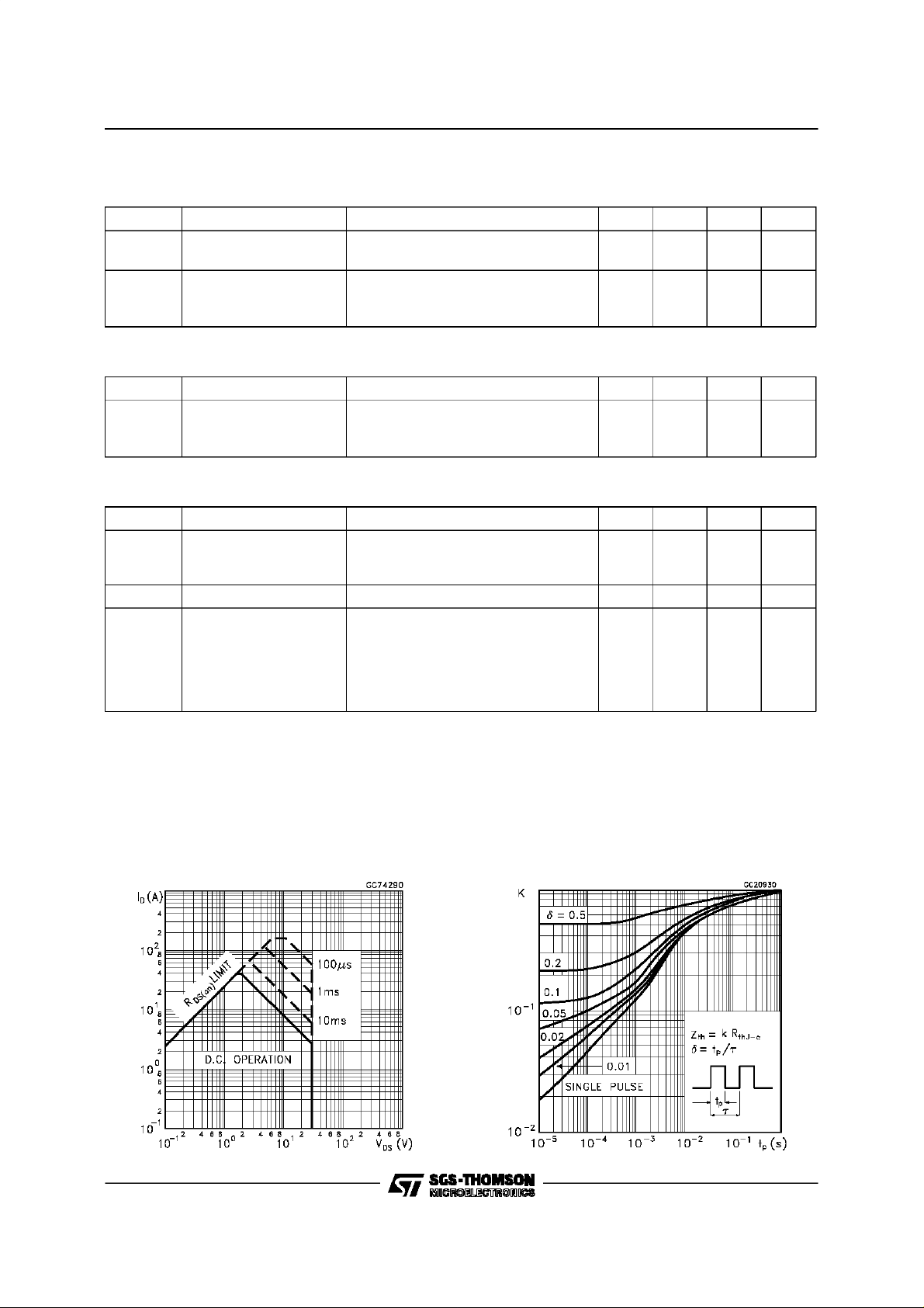
Safe Operating Area ThermalImpedance
3/8
Page 4

STP40NE03L-20
OutputCharacteristics
Transconductance
TransferCharacteristics
StaticDrain-sourceOn Resistance
GateCharge vs Gate-sourceVoltage
4/8
CapacitanceVariations
Page 5

STP40NE03L-20
Normalized Gate Threshold Voltage vs
Temperature
Source-drainDiode Forward Characteristics
Normalized On Resistance vs Temperature
5/8
Page 6

STP40NE03L-20
Fig. 1: Unclamped Inductive Load Test Circuit
Fig. 3: SwitchingTimes Test CircuitsFor
ResistiveLoad
Fig. 2: Unclamped Inductive Waveform
Fig. 4: Gate Charge test Circuit
Fig. 5: Test Circuit For InductiveLoad Switching
And Diode RecoveryTimes
6/8
Page 7

TO-220 MECHANICAL DATA
STP40NE03L-20
DIM.
MIN. TYP. MAX. MIN. TYP. MAX.
A 4.40 4.60 0.173 0.181
C 1.23 1.32 0.048 0.051
D 2.40 2.72 0.094 0.107
D1 1.27 0.050
E 0.49 0.70 0.019 0.027
F 0.61 0.88 0.024 0.034
F1 1.14 1.70 0.044 0.067
F2 1.14 1.70 0.044 0.067
G 4.95 5.15 0.194 0.203
G1 2.4 2.7 0.094 0.106
H2 10.0 10.40 0.393 0.409
L2 16.4 0.645
L4 13.0 14.0 0.511 0.551
L5 2.65 2.95 0.104 0.116
L6 15.25 15.75 0.600 0.620
L7 6.2 6.6 0.244 0.260
L9 3.5 3.93 0.137 0.154
DIA. 3.75 3.85 0.147 0.151
mm inch
E
A
L4
D
F2
F1
G1
H2
G
F
C
D1
L2
Dia.
L5
L7
L6
L9
P011C
7/8
Page 8

STP40NE03L-20
Informationfurnished is believed to be accurate and reliable.However, SGS-THOMSON Microelectronics assumes no responsability for the
consequencesof use of such informationnor for any infringementof patents or otherrights of thirdparties which may results fromits use.No
license isgranted byimplication orotherwise under anypatentor patentrights ofSGS-THOMSONMicroelectronics. Specifications mentioned
in this publicationare subject tochange without notice. This publicationsupersedes and replaces all informationpreviously supplied.
SGS-THOMSON Microelectronicsproductsare notauthorizedforuse ascriticalcomponents inlifesupportdevices orsystems withoutexpress
written approvalof SGS-THOMSONMicroelectonics.
1997 SGS-THOMSON Microelectronics -Printed in Italy- All RightsReserved
Australia- Brazil - Canada- China- France- Germany- Hong Kong - Italy- Japan- Korea -Malaysia - Malta - Morocco -The Netherlands -
Singapore - Spain- Sweden - Switzerland - Taiwan -Thailand - UnitedKingdom - U.S.A
SGS-THOMSON MicroelectronicsGROUP OF COMPANIES
...
8/8
 Loading...