

Page 1
STP3NA100
STP3NA100FI
N - CHANNEL ENHANCEMENT MODE
FAST POWER MOS TRANSISTOR
■ TYPICALR
DS(on)
=4.3 Ω
■ ± 30V GATE TO SOURCE VOLTAGERATING
■ 100% AVALANCHETESTED
■ REPETITIVEAVALANCHE DATA AT 100
o
C
■ LOWINTRINSICCAPACITANCES
■ GATECHARGEMINIMIZED
■ REDUCEDTHRESHOLD VOLTAGESPREAD
APPLICATIONS
■ HIGH CURRENT, HIGHSPEEDSWITCHING
■ SWITCHMODEPOWER SUPPLIES(SMPS)
■ DC-ACCONVERTERS FOR WELDING
EQUIPMENTAND UNINTERRUPTIBLE
POWERSUPPLIES AND MOTORDRIVE
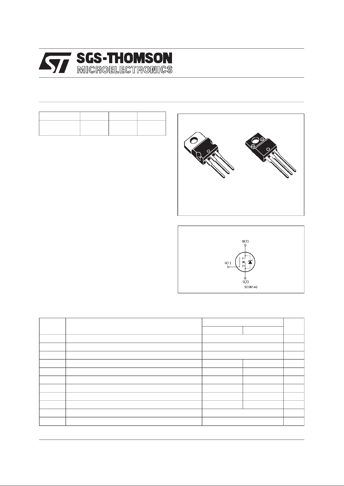
INTERNAL SCHEMATIC DIAGRAM
February 1998
TO-220 TO-220FI
1
2
3
1
2
3
ABSOLUTE MAXIMUM RATINGS
Symb o l Para meter Value Uni t
ST P3NA100 STP3N A100FI
V
DS
Drain-source Voltage (VGS= 0) 1000 V
V
DGR
Drain- gate Voltage (RGS=20kΩ)
1000 V
V
GS
Gat e- source Voltage ± 30 V
I
D
Drain Current (continuous ) at Tc=25oC3.52.0A
I
D
Drain Current (continuous ) at Tc=100oC2.01.2A
I
DM
(•) Drain Current (pulsed ) 14 14 A
P
tot
Tot al Dissip at i on at Tc=25oC11045W
Derat in g F actor 0.88 0.36 W/
o
C
V
ISO
Ins ulation Withs t a nd Volt age (DC) 2000 V
T
stg
Sto rage Temperature -65 to 150
o
C
T
j
Max. Oper at in g Junc t io n Temper at ure 150
o
C
(•) Pulsewidth limitedby safe operating area
TYPE V
DSS
R
DS(on)
I
D
STP3NA100
ST P3NA100F I
1000 V
1000 V
<5 Ω
<5Ω
3.5 A
2A
1/9
Page 2
THERMAL DATA
TO-220 IS O WATT 220
R
thj-case
Ther mal Resist ance Junction-c a s e Max 1.14 2.78
o
C/W
R
thj-amb
R
thc-sin k
T
l
Ther mal Resist ance Junction-ambient Max
Ther mal Resist ance Case-sink Ty p
Maximum Lead T e mperature For Sold eri ng P ur p os e
62.5
0.5
300
o
C/W
o
C/W
o
C
AVALANCHE CHARACTERISTICS
Symbol Parameter Max Va lue Uni t
I
AR
Avalanche Curre nt , Repet it ive or Not -Re petitive
(pulse width limited by T
j
max, δ <1%)
3.5 A
E
AS
Single Pulse Avalanche Energy
(starting T
j
=25oC, ID=IAR,VDD=50V)
170 mJ
ELECTRICAL CHARACTERISTICS (T
case
=25oC unlessotherwise specified)
OFF
Symbol Parameter Test Cond itions Min. Typ. Max. Unit
V
(BR)DSS
Drain-source
Breakdown Volt age
I
D
=250µAVGS=0
1000 V
I
DSS
Zer o Gate V o lt age
Drain Cur re nt (V
GS
=0)
V
DS
=MaxRating
V
DS
=MaxRating Tc=125oC
25
250
µA
µA
I
GSS
Gat e-body Leakage
Current (V
DS
=0)
V
GS
= ± 30 V
± 100 nA
ON (∗)
Symbol Parameter Test Cond itions Min. Typ. Max. Unit
V
GS(th )
Gate Threshold
Voltage
V
DS=VGSID
=250µA
2.25 3 3.75 V
R
DS(on)
Stati c D rain-source On
Resistance
VGS=10V ID= 1.5 A 4.3 5 Ω
I
D(on)
On State Drain Cu r rent VDS>I
D(on)xRDS(on)max
VGS=10V
3.5 A
DYNAMIC
Symbol Parameter Test Cond itions Min. Typ. Max. Unit
g
fs
(∗)Forward
Tr ansconductance
VDS>I
D(on)xRDS(on)maxID
=1.5A 1.5 3 S
C
iss
C
oss
C
rss
Input Capaci t an c e
Out put Capa c itance
Reverse Transfer
Capa cit an c e
VDS=25V f=1MHz VGS= 0 1100
85
20
1430
110
30
pF
pF
pF
STP3NA100/FI
2/9
Page 3
ELECTRICAL CHARACTERISTICS (continued)
SWITCHINGON
Symbol Parameter Test Cond itions Min. Typ. Max. Unit
t
d(on)
t
r
Turn-on Time
Rise Tim e
VDD=500V ID=1.7A
R
G
=4.7 Ω VGS=10V
20
27
27
35
ns
ns
Q
g
Q
gs
Q
gd
Total Gate Charge
Gat e-Source Charge
Gate-Drain Charge
VDD=800V ID=3.5A VGS=10V 48
8
23
65 nC
nC
nC
SWITCHINGOFF
Symbol Parameter Test Cond itions Min. Typ. Max. Unit
t
r(Voff)
t
f
t
c
Of f - voltage Rise T im e
Fall Time
Cross-over Tim e
VDD=800V ID=3.5A
R
G
=47 Ω VGS=10V
(see test circuit, figure 5)
62
22
95
85
30
125
ns
ns
ns
SOURCE DRAIN DIODE
Symbol Parameter Test Cond itions Min. Typ. Max. Unit
I
SD
I
SDM
(•)
Source-drain Current
Source-drain Current
(pulsed)
3.5
14
A
A
V
SD
(∗) For ward On Vo lt age ISD=3.5A VGS=0 1.6 V
t
rr
Q
rr
I
RRM
Reverse Recovery
Time
Reverse Recovery
Charge
Reverse Recovery
Current
I
SD
= 3.5 A di/dt = 100 A/µs
V
DD
=100V Tj=150oC
(see circuit, figure 5)
1000
15
35
ns
µC
A
(∗) Pulsed: Pulse duration =300 µs,duty cycle 1.5 %
(•) Pulse width limited by safe operating area
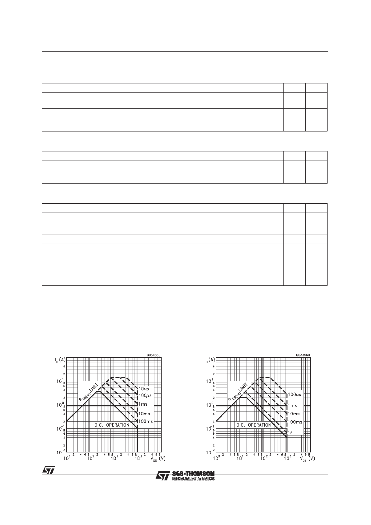
Safe Operating Areafor TO-220 Safe Operating Area for TO-220FP
STP3NA100/FI
3/9
Page 4

ThermalImpedance for TO-220
OutputCharacteristics
Transconductance
ThermalImpedance forTO-220FP
TransferCharacteristics
StaticDrain-sourceOn Resistance
STP3NA100/FI
4/9
Page 5

GateCharge vs Gate-sourceVoltage
Normalized Gate Threshold Voltage vs
Temperature
Source-drainDiode Forward Characteristics
CapacitanceVariations
Normalized On Resistance vs Temperature
STP3NA100/FI
5/9
Page 6

Fig. 1: Unclamped InductiveLoad Test Circuit
Fig. 3: SwitchingTimes Test Circuits For
ResistiveLoad
Fig. 2: Unclamped Inductive Waveform
Fig. 4: Gate Charge test Circuit
Fig. 5: Test Circuit For Inductive Load Switching
And Diode RecoveryTimes
STP3NA100/FI
6/9
Page 7

DIM.
mm inch
MIN. TYP. MAX. MIN. TYP. MAX.
A 4.40 4.60 0.173 0.181
C 1.23 1.32 0.048 0.051
D 2.40 2.72 0.094 0.107
D1 1.27 0.050
E 0.49 0.70 0.019 0.027
F 0.61 0.88 0.024 0.034
F1 1.14 1.70 0.044 0.067
F2 1.14 1.70 0.044 0.067
G 4.95 5.15 0.194 0.203
G1 2.4 2.7 0.094 0.106
H2 10.0 10.40 0.393 0.409
L2 16.4 0.645
L4 13.0 14.0 0.511 0.551
L5 2.65 2.95 0.104 0.116
L6 15.25 15.75 0.600 0.620
L7 6.2 6.6 0.244 0.260
L9 3.5 3.93 0.137 0.154
DIA. 3.75 3.85 0.147 0.151
L6
A
C
D
E
D1
F
G
L7
L2
Dia.
F1
L5
L4
H2
L9
F2
G1
TO-220 MECHANICAL DATA
P011C
STP3NA100/FI
7/9
Page 8

DIM.
mm inch
MIN. TYP. MAX. MIN. TYP. MAX.
A 4.4 4.6 0.173 0.181
B 2.5 2.7 0.098 0.106
D 2.5 2.75 0.098 0.108
E 0.4 0.7 0.015 0.027
F 0.75 1 0.030 0.039
F1 1.15 1.7 0.045 0.067
F2 1.15 1.7 0.045 0.067
G 4.95 5.2 0.195 0.204
G1 2.4 2.7 0.094 0.106
H 10 10.4 0.393 0.409
L2 16 0.630
L3 28.6 30.6 1.126 1.204
L4 9.8 10.6 0.385 0.417
L6 15.9 16.4 0.626 0.645
L7 9 9.3 0.354 0.366
Ø 3 3.2 0.118 0.126
L2
A
B
D
E
H
G
L6
¯
F
L3
G1
123
F2
F1
L7
L4
ISOWATT220MECHANICAL DATA
P011G
STP3NA100/FI
8/9
Page 9

Information furnished is believed to be accurate and reliable. However, SGS-THOMSON Microelectronics assumes no responsability for the
consequences of use of such information nor for any infringement of patents orother rightsof third parties which may resultsfrom its use. No
license is granted by implication or otherwise under any patent orpatent rights of SGS-THOMSON Microelectronics. Specifications mentioned
in thispublication are subject to change without notice. This publication supersedes and replaces all information previously supplied.
SGS-THOMSON Microelectronics products are not authorized for useas criticalcomponentsin life support devices or systems without express
written approval ofSGS-THOMSON Microelectonics.
1998 SGS-THOMSON Microelectronics - Printed in Italy - All Rights Reserved
SGS-THOMSON Microelectronics GROUP OF COMPANIES
Australia - Brazil - Canada - China - France - Germany - Italy - Japan - Korea - Malaysia - Malta - Morocco - The Netherlands -
Singapore - Spain - Sweden - Switzerland - Taiwan - Thailand - United Kingdom - U.S.A
...
STP3NA100/FI
9/9
 Loading...