

Page 1
STP38N06
N - CHANNEL ENHANCEMENT MODE
”ULTRA HIGH DENSITY” POWER MOS TRANSISTOR
PRELIMINARY DATA
TYPE V
DSS
STP38N06 60 V < 0.03 Ω 38 A (*)
R
DS(on)
I
D
■ TYPICALR
■ AVALANCHERUGGEDTECHNOLOGY
■ 100% AVALANCHETESTED
■ REPETITIVEAVALANCHEDATAAT 100
■ HIGH CURRENTCAPABILITY
o
■ 175
■ HIGH dV/dt RUGGEDNESS
■ APPLICATIONORIENTED
COPERATINGTEMPERATURE
DS(on)
=0.026 Ω
o
C
CHARACTERIZATION
APPLICATIONS
■ HIGH CURRENT, HIGH SPEEDSWITCHING
■ POWERMOTOR CONTROL
■ DC-DC& DC-AC CONVERTERS
■ SYNCRONOUSRECTIFICATION
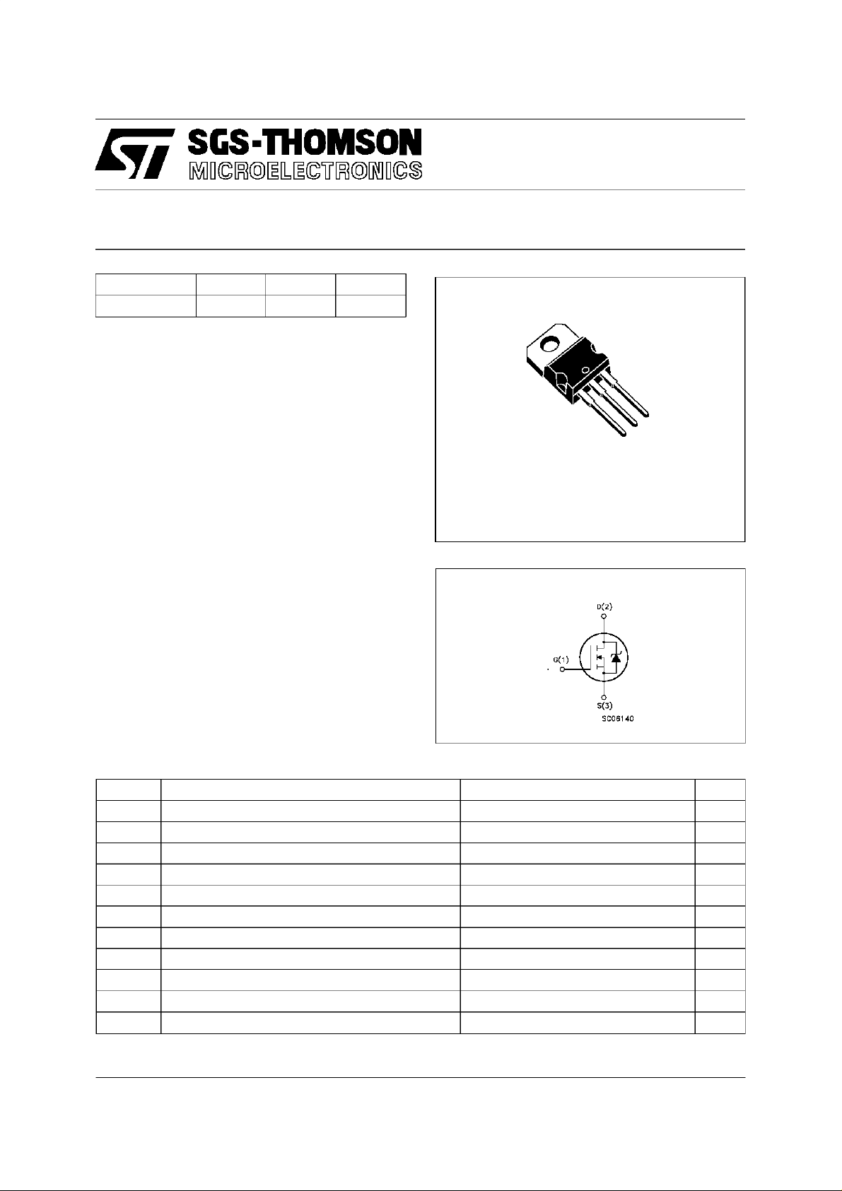
3
2
1
TO-220
INTERNAL SCHEMATIC DIAGRAM
ABSOLUTE MAXIMUM RATINGS
Symb o l Parame t er Val u e Uni t
V
V
DGR
V
I
DM
P
dV/dt(
T
(•) Pulse width limited by safe operating area
March 1996
Drain-source Voltage (VGS=0) 60 V
DS
Drain- gate Voltage (RGS=20kΩ)60V
Gate-source Voltage ± 20 V
GS
I
Drain Current (c ont inuo us) a t Tc=25oC38A
D
I
Drain Current (c ont inuo us) a t Tc=100oC26A
D
(•) Drain Current (puls ed) 152 A
Total Dissipat i on at Tc=25oC90W
tot
Derat ing Factor 0.6 W/
1) Peak Diode Recovery voltage slope 7 V/ns
Stora ge Temperature -65 to 175
stg
T
Max. Operat ing Junct i on Temperatu re 175
j
o
o
o
C
C
C
1/11
Page 2
STP38N06
THERMAL DATA
R
thj-case
R
thj-amb
R
thc-sin k
T
AVALANCHE CHARACTERISTICS
Symb o l Para met er Max V alue Uni t
I
AR
E
E
I
AR
Ther mal Resistance Junct ion-case Max
Ther mal Resistance Junct ion-ambient Max
Ther mal Resistance Case-s i nk Typ
Maximum Lead Tempera t ure For Solder ing Purpo se
l
Avalanche Current , Repet it iv e or Not-Repe t it ive
(pulse width limi t ed by T
Single Pu lse Avalanc he E nerg y
AS
(starti ng T
Repetitive Avalanche Energy
AR
=25oC, ID=IAR,VDD=25V)
j
(pulse width limi t ed by T
max, δ <1%)
j
max, δ <1%)
j
Avalanche Current , Repet it iv e or Not-Repe t it ive
=100oC, p ulse wid t h limited by Tjmax, δ <1%)
(T
c
1.66
62.5
0.5
300
38 A
300 mJ
75 mJ
26 A
o
C/W
o
C/W
o
C/W
o
C
ELECTRICAL CHARACTERISTICS (T
=25oC unlessotherwise specified)
case
OFF
Symbol Parameter Test Condition s Min. Typ. Max. Unit
V
(BR)DSS
Drain-source
ID= 250 µAVGS=0 60 V
Break dow n Voltage
I
I
DSS
GSS
Zero Gate Voltage
Drain Current (V
GS
Gat e- bod y Leaka ge
Current (V
DS
=0)
=0)
=MaxRating
V
DS
V
=MaxRatingx0.8 Tc= 125oC
DS
V
= ± 20 V ± 100 nA
GS
250
1000µAµA
ON (∗)
Symbol Parameter Test Condition s Min. Typ. Max. Unit
V
GS(th )
R
DS(on)
I
D(on)
Gat e Thre shold Volt age VDS=VGSID=250µA234V
St at ic Drain-source On
Resistance
VGS= 10V ID=19A
= 10V ID=19A Tc=100oC
V
GS
On State Drain Current VDS>I
D(on)xRDS(on)max
0.026 0.03
0.06
38 A
VGS=10V
DYNAMIC
Symbol Parameter Test Condition s Min. Typ. Max. Unit
g
(∗)Forward
fs
Tr ansc on ductance
C
C
C
Input Capac it an ce
iss
Out put Capac itance
oss
Reverse Transfer
rss
Capacit a nc e
VDS>I
D(on)xRDS(on)maxID
=19A 14 19 S
VDS=25V f=1MHz VGS= 0 2000
350
80
2800
450
120
Ω
Ω
pF
pF
pF
2/11
Page 3
STP38N06
ELECTRICAL CHARACTERISTICS (continued)
SWITCHINGON
Symbol Parameter Test Condition s Min. Typ. Max. Unit
t
d(on)
t
r
Turn-on Time
Rise Time
VDD=30V ID=19A
=50 Ω VGS=10V
R
G
(see test cir cuit, figure 3)
(di/dt)
Tur n-on C urr ent Slope VDD=48V ID=38A
on
R
=50 Ω VGS=10V
G
(see test cir cuit, figure 5)
Q
Q
Q
Tot al Gat e Charge
g
Gate-Source Charge
gs
Gat e- Drain Charge
gd
VDD=40V ID=38A VGS=10V 60
SWITCHINGOFF
Symbol Parameter Test Condition s Min. Typ. Max. Unit
t
r(Voff)
t
Off -voltage Rise Time
t
Fall T ime
f
Cross-over Time
c
VDD=48V ID=38A
=50 Ω VGS=10V
R
G
(see test cir cuit, figure 5)
SOURCE DRAIN DIODE
45
28065380
240 A/ µs
80 nC
10
20
65
140
230
85
180
300
ns
ns
nC
nC
ns
ns
ns
Symbol Parameter Test Condition s Min. Typ. Max. Unit
I
I
SDM
SD
Source-drain Current
(•)
Source-drain Current
38
152
(pulsed)
(∗)ForwardOnVoltage ISD=38A VGS=0 1.5 V
V
SD
t
Q
Reverse Recovery
rr
Time
Reverse Recovery
rr
ISD= 38 A di/dt = 10 0 A/µs
=40V Tj= 150oC
V
DD
(see test cir cuit, figure 5)
85
0.3
Charge
I
RRM
Reverse Recovery
7
Current
(∗) Pulsed: Pulse duration =300 µs,duty cycle 1.5 %
(•) Pulse width limited by safe operating area
(
1)I
≤ 20 A, di/dt≤ 300 A/µs, VDD≤ V
SD
(BR)DSS,Tj≤TJMAX
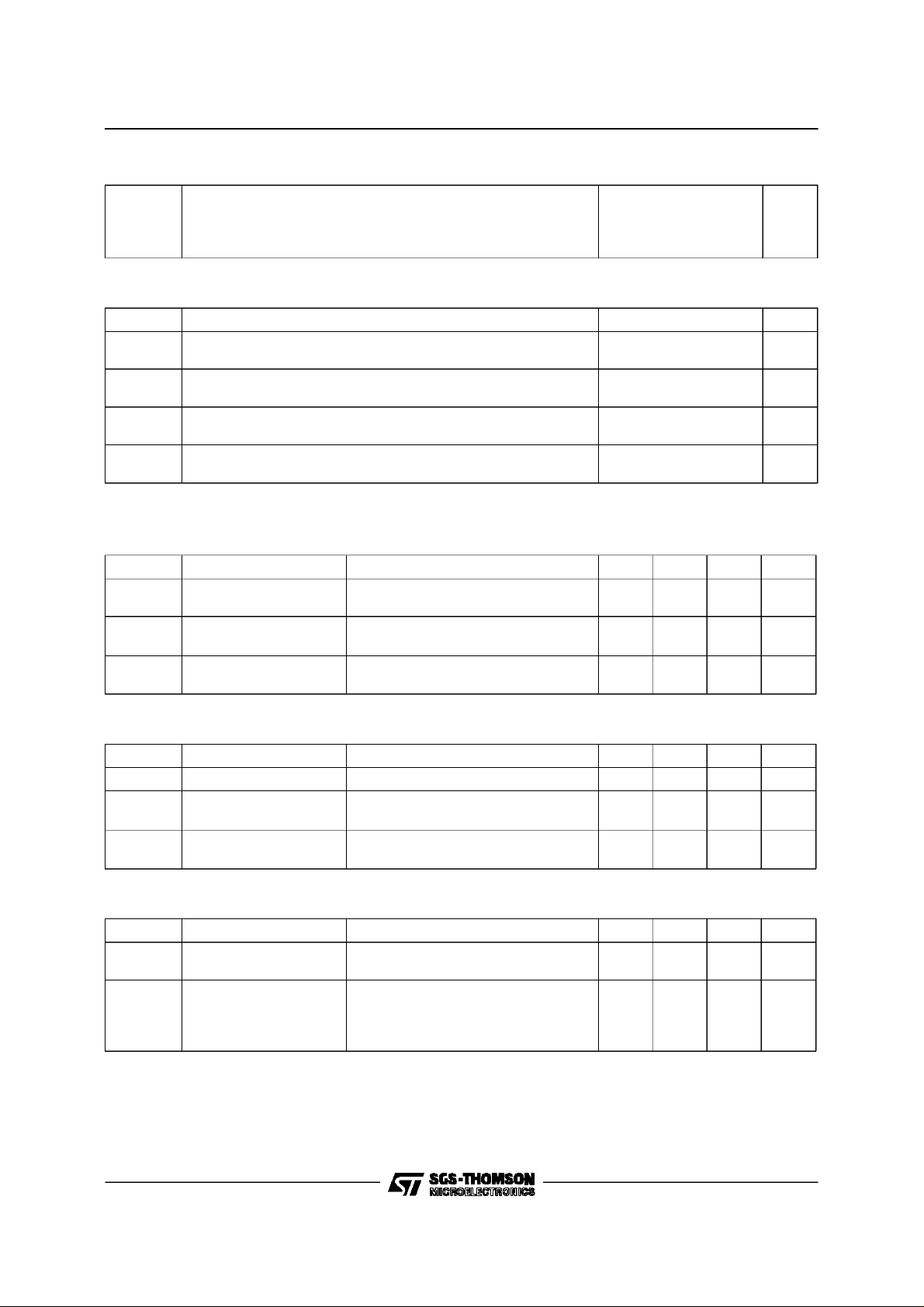
Safe Operating Area ThermalImpedance
A
A
ns
µC
A
3/11
Page 4
STP38N06
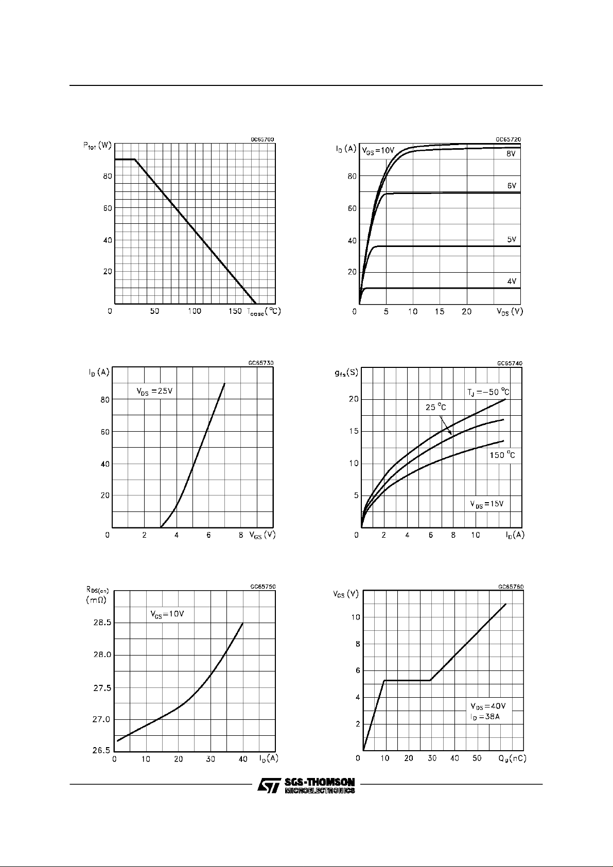
Derating Curve
TransferCharacteristics
OutputCharacteristics
Transconductance
StaticDrain-source On Resistance
4/11
Gate Charge vs Gate-source Voltage
Page 5

STP38N06
CapacitanceVariations
Normalized OnResistance vs Temperature
Normalized GateThreshold Voltage vs
Temperature
Turn-onCurrent Slope
Turn-offDrain-source VoltageSlope
Cross-overTime
5/11
Page 6

STP38N06
SwitchingSafe Operating Area
Source-drainDiode Forward Characteristics
AccidentalOverload Area
Fig. 1: UnclampedInductive Load Test Circuit
6/11
Fig. 2: UnclampedInductive Waveform
Page 7

STP38N06
Fig. 3: SwitchingTimes Test Circuits For
ResistiveLoad
Fig. 5: Test CircuitFor Inductive Load Switching
And DIodeRecovery Times
Fig. 4: GateCharge test Circuit
7/11
Page 8

STP38N06
PSPICEPARAMETERS
SUBCIRCUITCOMPONENTS
Symb o l Para met er Val ue Uni t
S1 (V 14_16<0) ( S ee Power Mosf et Model Subcir cuit ) O N
S2 (V 16_11<0) ( S ee Power Mosf et Model Subcir cuit ) O N
LD Drain Inductance 8 nH
LG Gat e Induct ance 10 nH
LS Sour ce Inductance 10 nH
RDRAI N Drain Resistanc e 1.9E
RGA T E Gat e Resist ance 1 Ω
CGD Gate Drain Capacitance 3.92 nF
CGS Gate Source Capacit anc e 1.9 nF
ALF A Dr if t Coef icient 1E
RGN Negative Bias Resis t a nc e 10 KΩ
DIODE DRAIN GATE (Depletion Capacitance)
Symb o l Para met er Val ue Uni t
CJO Z e r o Bias p- n Capacitance 2.6 nF
VJ p- n Potential 0.1 V
M p-n Grading Coefficient 0.6
-2
-3
Ω
-1
V
DIODE DRAIN SOURCE
Symb o l Para met er Val ue Uni t
CJO Z e r o Bias p- n Capacitance 7.8 nF
VJ p- n Potential 0.1 V
M p-n Grading Coefficient 0.6
TT Tr ans it Time 20 nsec
N MOSFET
Symb o l Para met er Val ue Uni t
L Channel Length 1 µ Meter
W Ch annel Widt h 1 µ Meter
LEVEL Model Index 3
TOX Oxide Thickness 1 Meter
VT O Ze ro Bias Threshold Vo lt age 3.25 V
U0 Surf ac e Mobility 600 cm
THE T A Mobilit y M odulat i on 0.005 V
Vmax Maximum Drift Velocity 0 Meter/sec
KP Trans Conduct ance Coeff ic i ent 28 Amp/ V
For Transient Simulation Applicate U.I.C. (Use Initial Condition) Option
2
/VS
-1
2
8/11
Page 9

STP38N06
PSPICENETLIST OF THE SUBCIRCUIT
.S UB CKT ST P38N06 1 2 3
*VALUE OF THE PACKAGE IN DUCTANC ES
LS 1 11 10n
LG 2 12 10n
LD 3 13 7n
*RESISTANCE OF THEGATE
PO LYSILI CO N
RG 12 16 1
*EPY AND DRIFT RESISTANC ES
RD 13 14 1.9e-02
EDRI 14 15 POL Y (2 ) (13 14) (13 1 1) 0 0 0 0
1e-3
*CAPAC ITANCE GATE SO UR CE
CGS16111.90n
*OPTIO NAL FO R NEGATIVE GATE BIAS
*S251111116SWITCH
*CGN 51 16 3.92n
*RGN 51 16 10k
*MILLER CAPACIT A NCE
CGD 16 17 3.92n
PowerMosfet ModelSubcircuit
* DEPLETION CAPACITANCE
DGD 17 14 DGD
S1 17 14 16 14 SWI T CH
.MODEL DGDD +IS=
+CJO =2. 6n
+Vj=.1
+M=.6
.MOD EL SWITCH VSW ITCH
+RON=1m
+ROFF=1MEG
+VON=0.1
* OU TP UT CAPACITANC E AND BODY DRAI N DI ODE
DBD 11 14 DBD
.MODEL DBDD
+TT=20n
+CJO =7. 8n
+VJ=.1
+M=.6
* MODELOF THE MOSFET
MMAIN 1 5 16 11 11 MM AIN L=1u W =1u
.MOD EL MMAIN NMOS
+LEVEL= 3
+TOX=1
+VTO=3.25
+uo=600
+THETA=0.005
+VM AX=5e7
+KP= 28
.ENDS
9/11
Page 10

STP38N06
TO-220 MECHANICAL DATA
DIM.
MIN. TYP. MAX. MIN. TYP. MAX.
A 4.40 4.60 0.173 0.181
C 1.23 1.32 0.048 0.051
D 2.40 2.72 0.094 0.107
D1 1.27 0.050
E 0.49 0.70 0.019 0.027
F 0.61 0.88 0.024 0.034
F1 1.14 1.70 0.044 0.067
F2 1.14 1.70 0.044 0.067
G 4.95 5.15 0.194 0.203
G1 2.4 2.7 0.094 0.106
H2 10.0 10.40 0.393 0.409
L2 16.4 0.645
L4 13.0 14.0 0.511 0.551
L5 2.65 2.95 0.104 0.116
L6 15.25 15.75 0.600 0.620
L7 6.2 6.6 0.244 0.260
L9 3.5 3.93 0.137 0.154
DIA. 3.75 3.85 0.147 0.151
mm inch
E
A
L4
D
F2
F1
G1
H2
G
F
C
D1
L2
Dia.
L5
L7
L6
L9
P011C
10/11
Page 11

STP38N06
Information furnished is believedto be accurateand reliable. However, SGS-THOMSON Microelectronics assumes no responsability for the
consequencesof use ofsuch informationnor for any infringement of patents or otherrights of third parties which may resultsfrom its use. No
licenseis grantedby implicationor otherwise underany patentor patentrights ofSGS-THOMSONMicroelectronics. Specificationsmentioned
in this publicationare subject to change without notice.This publication supersedes and replaces all information previously supplied.
SGS-THOMSONMicroelectronics productsarenotauthorized for useas critical components in lifesupportdevices or systemswithoutexpress
writtenapproval of SGS-THOMSONMicroelectonics.
1995 SGS-THOMSONMicroelectronics - All Rights Reserved
Australia - Brazil- France - Germany - HongKong - Italy- Japan- Korea - Malaysia - Malta - Morocco- The Netherlands -
Singapore- Spain- Sweden - Switzerland- Taiwan - Thailand - United Kingdom- U.S.A
SGS-THOMSONMicroelectronicsGROUPOF COMPANIES
...
11/11
 Loading...