

Page 1
STP36NE06
N - CHANNEL 60V - 0.032Ω - 36A - TO-220/TO-220FP
TYPE V
STP36NE06
STP36NE06FP
■ TYPICALR
■ EXCEPTIONAL dv/dt CAPABILITY
■ 100% AVALANCHETESTED
■ LOW GATE CHARGE 100
■ APPLICATIONORIENTED
DS(on)
DSS
60 V
60 V
=0.032 Ω
CHARACTERIZATION
DESCRIPTION
This Power Mosfet is the latest development of
SGS-THOMSON unique ”Single Feature Size”
strip-based process. The resulting transistor
shows extremelyhigh packing density for low onresistance, rugged avalance characteristics and
less critical alignment steps therefore a remarkable manufacturingreproducibility.
R
DS(on)
<0.040Ω
<0.040Ω
o
C
I
D
36 A
20 A
STP36NE06FP
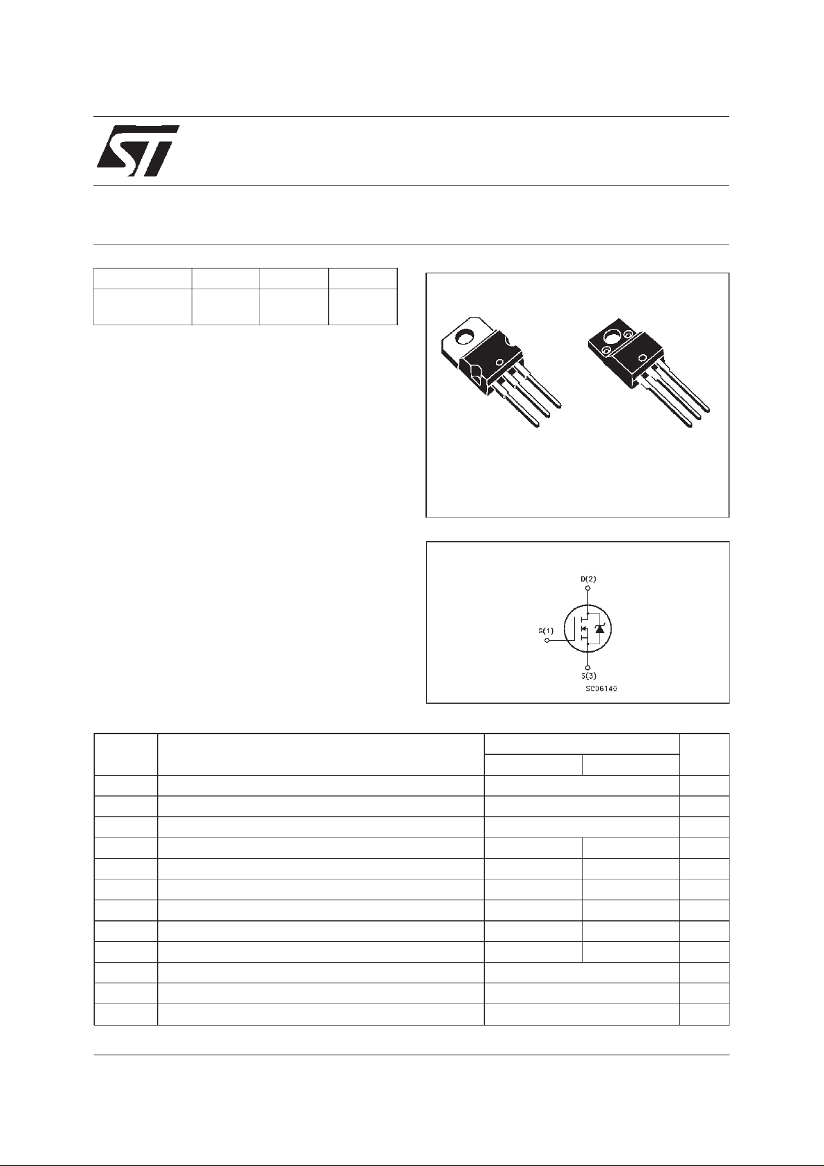
STripFET POWER MOSFET
3
2
1
TO-220 TO-220FP
INTERNAL SCHEMATIC DIAGRAM
3
2
1
APPLICATIONS
■ HIGH CURRENT, HIGH SPEEDSWITCHING
■ SOLENOIDANDRELAY DRIVERS
■ MOTORCONTROL, AUDIOAMPLIFIERS
■ DC-DC& DC-AC CONVERTERS
ABSOLUTE MAXIMUM RATINGS
Symb o l Para meter Value Uni t
STP 36NE06 STP36NE06 F P
V
V
V
I
DM
P
V
dv/ dt Peak Diode Re c overy voltage slope 7 V/ns
T
(•) Pulsewidth limitedby safe operatingarea (1)ISD≤ 36 A,di/dt ≤ 300 A/µs, VDD≤ V
July 1998
Drain-source Voltage (VGS=0) 60 V
DS
Drain- gate Voltage ( RGS=20kΩ)
DGR
Gat e- source Voltage ± 20 V
GS
I
Drain Current (cont in uous) at Tc=25oC3620A
D
I
Drain Current (cont in uous) at Tc=100oC2414A
D
60 V
(•) Drain Current (pulsed ) 144 144 A
Tot al Dissipat i on at Tc=25oC10035W
tot
Derat in g Factor 0.66 0.27 W/
Ins ulation Withst and Voltage (DC) 2000 V
ISO
Sto rage T emperat ure -65 to 17 5
stg
T
Max. Operat in g Junct io n Temper at u r e 175
j
(BR)DSS,Tj≤TJMAX
o
C
o
C
o
C
1/9
Page 2
STP36NE06FP
THERMAL DATA
TO - 2 20 TO-220FP
R
thj-case
R
thj-amb
R
thc-sin k
T
AVALANCHE CHARACTERISTICS
Symbol Paramet e r Max Value Uni t
I
AR
E
Ther mal Resistan ce Junction-c a s e Max 1.51 4.28
Ther mal Resistan ce Junction-ambient Max
Ther mal Resistan ce Case - sink Ty p
Maximum Lead Te mperature For Soldering P urpose
l
Avalanche Curre nt, Repet it i v e or Not -Repetit ive
(pulse w idth limited b y T
Single Pulse Avalanche Energy
AS
(starting T
=25oC, ID=IAR,VDD=25V)
j
max)
j
62.5
0.5
300
36 A
180 mJ
o
C/W
o
C/W
o
C/W
o
C
ELECTRICAL CHARACTERISTICS (T
=25oC unlessotherwise specified)
case
OFF
Symbol Parameter Test Condition s Min. Typ. Max. Un it
V
(BR)DSS
Drain-source
=250µAVGS=0
I
D
60 V
Breakdown Volt age
I
DSS
I
GSS
Zer o Gate Volt age
Drain Curre nt (V
GS
Gat e-body Leakage
Current (V
DS
=0)
=0)
V
=MaxRating
DS
=MaxRating Tc=125
V
DS
o
C
= ± 20 V
V
GS
1
10
± 100 nA
ON (∗)
Symbol Parameter Test Condition s Min. Typ. Max. Un it
V
GS(th )
Gate Threshold
V
DS=VGSID
=250µA
234V
Voltage
R
DS(on)
Stati c Drain-so urce On
VGS=10V ID=18A 0.032 0.04 Ω
Resistance
I
D(on)
On State Drain Cu rr e nt VDS>I
D(on)xRDS(on)max
36 A
VGS=10V
DYNAMIC
Symbol Parameter Test Condition s Min. Typ. Max. Un it
g
(∗)Forward
fs
Tr ansconductance
C
C
C
Input Capacit ance
iss
Out put Capa citance
oss
Reverse Transfer
rss
Capa cit an c e
VDS>I
D(on)xRDS(on)maxID
=18 A 7 15 S
VDS=25V f=1MHz VGS= 0 2115
260
65
2800
350
90
µA
µA
pF
pF
pF
2/9
Page 3
STP36NE06FP
ELECTRICAL CHARACTERISTICS (continued)
SWITCHINGON
Symbol Parameter Test Condition s Min. Typ. Max. Un it
t
d(on)
t
r
(di/dt)
Q
Q
gs
Q
gd
Turn-on Time
Rise Time
Turn-on Current Slope VDD=48V ID=36A
on
Total Gate Charge
g
VDD=30V ID=18A
=4.7Ω VGS=10V
R
G
=4.7 Ω VGS=10 V
R
G
VDD=48V ID=36A VGS=10V 50
Gat e-Sourc e Charge
Gate-Drain Charge
28
85
250 A/µ s
13
18
SWITCHINGOFF
Symbol Parameter Test Condition s Min. Typ. Max. Un it
t
r(Voff)
t
t
Of f - voltage Rise Time
Fall Time
f
Cross-over Tim e
c
VDD=48V ID=36A
=4.7 Ω VGS=10V
R
G
12
25
40
SOURCE DRAIN DIODE
Symbol Parameter Test Condition s Min. Typ. Max. Un it
I
SD
I
SDM
V
SD
t
Q
I
RRM
(∗) Pulsed: Pulse duration =300 µs, duty cycle 1.5 %
(•) Pulse widthlimited by safe operating area
Source-drain Current
(•)
Source-drain Current
(pulsed)
(∗) Forward On Volt age ISD=36A VGS=0 1.5 V
Reverse Recover y
rr
Time
Reverse Recover y
rr
= 36 A di/dt = 10 0 A/µs
I
SD
=30V Tj=150oC
V
DD
75
245
Charge
Reverse Recover y
6.5
Current
40
115
70 nC
16
35
55
36
144
ns
ns
nC
nC
ns
ns
ns
A
A
ns
µC
A
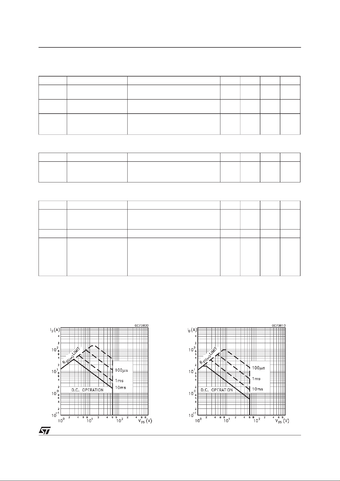
Safe Operating Areafor TO-220 Safe Operating Area for TO-220FP
3/9
Page 4

STP36NE06FP
ThermalImpedance for TO-220
OutputCharacteristics
ThermalImpedance forTO-220FP
TransferCharacteristics
Transconductance
4/9
StaticDrain-sourceOn Resistance
Page 5

STP36NE06FP
GateCharge vs Gate-sourceVoltage
Normalized GateThresholdVoltage vs
Temperature
CapacitanceVariations
Normalized On Resistancevs Temperature
Source-drainDiode Forward Characteristics
5/9
Page 6

STP36NE06FP
Fig. 1: UnclampedInductiveLoad Test Circuit
Fig. 3: Switching Times Test CircuitsFor
ResistiveLoad
Fig. 2: UnclampedInductive Waveform
Fig. 4: Gate Charge test Circuit
Fig. 5: Test Circuit For Inductive Load Switching
And Diode RecoveryTimes
6/9
Page 7

TO-220 MECHANICALDATA
STP36NE06FP
DIM.
MIN. TYP. MAX. MIN. TYP. MAX.
A 4.40 4.60 0.173 0.181
C 1.23 1.32 0.048 0.051
D 2.40 2.72 0.094 0.107
D1 1.27 0.050
E 0.49 0.70 0.019 0.027
F 0.61 0.88 0.024 0.034
F1 1.14 1.70 0.044 0.067
F2 1.14 1.70 0.044 0.067
G 4.95 5.15 0.194 0.203
G1 2.4 2.7 0.094 0.106
H2 10.0 10.40 0.393 0.409
L2 16.4 0.645
L4 13.0 14.0 0.511 0.551
L5 2.65 2.95 0.104 0.116
L6 15.25 15.75 0.600 0.620
L7 6.2 6.6 0.244 0.260
L9 3.5 3.93 0.137 0.154
DIA. 3.75 3.85 0.147 0.151
mm inch
E
A
L4
D
F2
F1
G1
H2
G
F
C
D1
L2
Dia.
L5
L7
L6
L9
P011C
7/9
Page 8

STP36NE06FP
TO-220FP MECHANICALDATA
DIM.
MIN. TYP. MAX. MIN. TYP. MAX.
A 4.4 4.6 0.173 0.181
B 2.5 2.7 0.098 0.106
D 2.5 2.75 0.098 0.108
E 0.45 0.7 0.017 0.027
F 0.75 1 0.030 0.039
F1 1.15 1.7 0.045 0.067
F2 1.15 1.7 0.045 0.067
G 4.95 5.2 0.195 0.204
G1 2.4 2.7 0.094 0.106
H 10 10.4 0.393 0.409
L2 16 0.630
L3 28.6 30.6 1.126 1.204
L4 9.8 10.6 0.385 0.417
L6 15.9 16.4 0.626 0.645
L7 9 9.3 0.354 0.366
Ø 3 3.2 0.118 0.126
mm inch
E
A
D
B
L3
L6
L7
¯
F1
F
G1
H
G
F2
123
L2
L4
8/9
Page 9

STP36NE06FP
Information furnished is believed tobe accurateand reliable. However,STMicroelectronicsassumes no responsibility for theconsequences
of use of such information nor for any infringement of patents or other rights of third parties which may result from its use. No license is
granted by implication orotherwise under any patentor patent rights of STMicroelectronics. Specification mentionedin this publication are
subject tochange without notice. This publication supersedes and replaces allinformation previously supplied. STMicroelectronics products
are not authorized for use as critical componentsin life support devices or systems withoutexpresswritten approvalof STMicroelectronics.
Australia - Brazil - Canada - China- France - Germany- Italy - Japan- Korea- Malaysia- Malta - Mexico - Morocco - TheNetherlands -
Singapore- Spain- Sweden - Switzerland- Taiwan -Thailand - United Kingdom- U.S.A.
The ST logo isa trademark of STMicroelectronics
1998 STMicroelectronics– Printed in Italy – All Rights Reserved
STMicroelectronicsGROUP OF COMPANIES
.
9/9
 Loading...