

Page 1

LED sink driver with output error detection
Features
■ Low voltage power supply down to 3 V
■ 16 constant current output channels
■ Adjustable output current through external
resistor
■ Short and open output error detection
■ Serial data IN/parallel data OUT
■ 3.3 V MCU-driving capability
■ Output current: 3 to 40 mA
■ 30 MHz clock frequency
■ Available in high thermal efficiency TSSOP
exposed pad
■ ESD protection: 2 kV HBM, 200 V MM
Description
The STP16DPP05 is a monolithic, low voltage,
low current power 16-bit shift register designed for
LED panel displays. The device features a 16-bit
serial-in, parallel-out shift register that feeds a
16-bit D-type storage register. In the output stage,
sixteen regulated current sources are designed to
provide 3 to 40 mA of constant current to drive the
LEDs. The STP16DPP05 features open and short
LED detection on the outputs. The detection
circuit checks for 3 different conditions that can
occur on the output line: short to GND, short to V
or open line.
Table 1. Device summary
O
STP16DPP05
Low voltage 16-bit constant current
QSOP-24
TSSOP24
The data detection results are loaded in the shift
registers and shifted out via the serial line output.
The detection functionality is implemented without
increasing the pin count, through a secondary
function of the output enable and latch pin (DM1
and DM2 respectively). A dedicated logic
sequence allows the device to enter or exit from
detection mode. The STP16DPP05 output current
can be adjusted through an external resistor to
control the light intensity of the LEDs.
LED brightness is adjustable from 0% to 100% via
the OE/DM2
pin.
The STP16DPP05 guarantees a 20 V output
driving capability, allowing users to connect more
LEDs in series. The high 30 MHz clock frequency
makes the device suitable for high data rate
transmission. The 3.3 V supply is well suited for
applications which interface a 3.3 V MCU.
Compared to a standard TSSOP package, the
TSSOP with exposed pad increases heat
dissipation capability by a factor of 2.5
SO-24
TSSOP24
(exposed pad)
Order codes Package Packaging
STP16DPP05MTR SO-24 (tape and reel) 1000 parts per reel
STP16DPP05TTR TSSOP24 (tape and reel) 2500 parts per reel
STP16DPP05XTTR
TSSOP24 exposed pad
(tape and reel)
2500 parts per reel
STP16DPP05PTR QSOP-24 2500 parts per reel
October 2009 Doc ID 16518 Rev 1 1/32
www.st.com
32
Page 2

Contents STP16DPP05
Contents
1 Summary description . . . . . . . . . . . . . . . . . . . . . . . . . . . . . . . . . . . . . . . . 3
1.1 Pin connection and description . . . . . . . . . . . . . . . . . . . . . . . . . . . . . . . . . 3
2 Electrical ratings . . . . . . . . . . . . . . . . . . . . . . . . . . . . . . . . . . . . . . . . . . . . 5
2.1 Absolute maximum ratings . . . . . . . . . . . . . . . . . . . . . . . . . . . . . . . . . . . . . 5
2.2 Thermal data . . . . . . . . . . . . . . . . . . . . . . . . . . . . . . . . . . . . . . . . . . . . . . . 5
2.3 Recommended operating conditions . . . . . . . . . . . . . . . . . . . . . . . . . . . . . 6
3 Electrical characteristics . . . . . . . . . . . . . . . . . . . . . . . . . . . . . . . . . . . . . 7
4 Equivalent circuit and outputs . . . . . . . . . . . . . . . . . . . . . . . . . . . . . . . . . 9
5 Timing diagrams . . . . . . . . . . . . . . . . . . . . . . . . . . . . . . . . . . . . . . . . . . . 11
6 Typical characteristics . . . . . . . . . . . . . . . . . . . . . . . . . . . . . . . . . . . . . . 14
7 Error detection mode functionality . . . . . . . . . . . . . . . . . . . . . . . . . . . . 18
7.1 Phase one: entering error detection mode . . . . . . . . . . . . . . . . . . . . . . . . 18
7.2 Phase two: error detection . . . . . . . . . . . . . . . . . . . . . . . . . . . . . . . . . . . . 19
7.3 Phase three: resuming normal mode . . . . . . . . . . . . . . . . . . . . . . . . . . . . 21
7.4 Error detection conditions . . . . . . . . . . . . . . . . . . . . . . . . . . . . . . . . . . . . . 21
8 Package mechanical data . . . . . . . . . . . . . . . . . . . . . . . . . . . . . . . . . . . . 23
9 Revision history . . . . . . . . . . . . . . . . . . . . . . . . . . . . . . . . . . . . . . . . . . . 31
2/32 Doc ID 16518 Rev 1
Page 3

STP16DPP05 Summary description
1 Summary description
Table 2. Typical current accuracy
Current accuracy
Output voltage
Between bits Between ICs
≥ 1.3 V ± 1% ± 2% 5 to 40 mA 3.3 V to 5 V 25 °C
1.1 Pin connection and description
Figure 1. Pin connection
Output current
V
DD
Temper atur e
Note: The exposed pad should be electrically connected to a metal land electrically isolated or
connected to ground.
Doc ID 16518 Rev 1 3/32
Page 4

Summary description STP16DPP05
Table 3. Pin description
Pin n° Symbol Name and function
1 GND Ground terminal
2 SDI Serial data input terminal
3 CLK Clock input terminal
4 LE/DM1 Latch input terminal - detect mode 1 (see operation principle)
5-20 OUT 0-15
Output terminal
21 OE/DM2
Input terminal of output enable (active low) - detect mode 1
(see operation principle)
22 SDO Serial data out terminal
23 R-EXT
24 V
DD
Input terminal for an external resistor for constant current
programming
Supply voltage terminal
4/32 Doc ID 16518 Rev 1
Page 5

STP16DPP05 Electrical ratings
2 Electrical ratings
2.1 Absolute maximum ratings
Stressing the device above the ratings listed in the “absolute maximum ratings” table may
cause permanent damage to the device. These are stress ratings only and operation of the
device at these or any other condition above those indicated in the operating sections of this
specification is not implied. Exposure to absolute maximum rating conditions for extended
periods may affect device reliability.
Table 4. Absolute maximum ratings
Symbol Parameter Value Unit
V
DD
V
I
O
V
I
GND
f
CLK
T
1. Such absolute value is based on the thermal shutdown protection.
Supply voltage 0 to 7 V
Output voltage -0.5 to 20 V
O
Output current 50 mA
Input voltage -0.4 to V
I
GND terminal current 800 mA
Clock frequency 50 MHz
Junction temperature range
J
2.2 Thermal data
Table 5. Thermal data
Symbol Parameter Value Unit
T
J-OPR
T
R
T
STG
thJA
Operating free-air temperature range -40 to +125 °C
A
Operating thermal junction temperature range -40 to +150 °C
Storage temperature range -55 to +150 °C
Thermal resistance junctionambient
(1)
(1)
DD
-40 to +170 °C
SO-24 42.7 °C/W
TSSOP24 55 °C/W
(2)
TSSOP24
Exposed Pad
37.5 °C/W
V
QSOP-24 55 °C/W
1. According with JEDEC standard 51-7B
2. The exposed pad should be soldered directly to the PCB to obtain the thermal benefits.
Doc ID 16518 Rev 1 5/32
Page 6

Electrical ratings STP16DPP05
2.3 Recommended operating conditions
Table 6. Recommended operating conditions
Symbol Parameter Test conditions Min. Typ. Max. Unit
V
V
I
I
V
V
t
wLAT
t
wCLK
t
wEN
t
SETUP(D)
t
HOLD(D)
t
SETUP(L)
f
CLK
Supply voltage 3.0 5.5 V
DD
Output voltage 20 V
O
Output current OUTn 3 40 mA
I
O
Output current SERIAL-OUT +1 mA
OH
Output current SERIAL-OUT -1 mA
OL
Input voltage 0.7 V
IH
Input voltage -0.3 0.3 V
IL
LE/DM1 pulse width
DD
20 ns
CLK pulse width 10 ns
OE/DM2 pulse width 100 ns
VDD = 3.0 V to 5.0 V
Setup time for DATA 8 ns
Hold time for DATA 5 ns
Setup time for LATCH 8 ns
Clock frequency Cascade operation
(1)
V
DD
30 MHz
1. If the device is connected in cascade, it may not be possible achieve the maximum data transfer.
Please consider the timings carefully.
DD
V
V
6/32 Doc ID 16518 Rev 1
Page 7

STP16DPP05 Electrical characteristics
3 Electrical characteristics
VDD = 3.3 V to 5 V, TA = 25 °C, unless otherwise specified.
Table 7. Electrical characteristics
Symbol Parameter Test conditions Min. Typ. Max. Unit
V
V
I
OH
V
V
I
OL1
OL2
I
OL3
ΔI
OL1
OL2
ΔI
OL3
R
SIN(up)
R
SIN(down)
I
DD(OFF1)
Input voltage high level 0.7 V
IH
Input voltage low level GND 0.3 V
IL
DD
Output leakage current VOH = 20 V 1 μA
Output voltage
OL
(serial-OUT)
Output voltage
OH
(serial-OUT)
Output current
Output current error
between bit
(All output ON)
= 1 mA 0.4 V
I
OL
= -1 mA VDD-0.4V V
I
OH
= 0.3 V, R
V
O
VO = 0.3 V, R
VO = 1.3 V, R
VO = 0.3 V, IO = 5 mA
= 4 kΩ
R
EXT
VO = 0.3 V, IO = 20 mA
R
= 980 Ω
EXT
VO = 1.3 V, IO = 40 mA
R
= 490 Ω
EXT
= 4 kΩ 4.75 5 5.25
ext
= 1 kΩ 19 20 21
ext
= 497 Ω 38 40 42
ext
± 1 ± 5
± 0.5 ± 3
± 0.5 ± 3
Pull-up resistor 150 300 600 kΩ
Pull-down resistor 100 200 400 kΩ
R
= 1 kΩ,
EXT
I
= 20 mA,
OUT
5.4 7.5
V
DD
DD
OUT 0 to 15 = OFF
Supply current (OFF)
R
= 497 Ω,
I
DD(OFF2)
EXT
= 40 mA OUT 0 to
I
OUT
8.0 9.5
15 = OFF
R
= 1 kΩ,
I
DD(ON1)
I
OUT
EXT
= 20 mA,
5.5 7.5
OUT 0 to 15 = ON
Supply current (ON)
R
= 497 Ω,
I
DD(ON2)
EXT
I
= 40 mA OUT 0 to
OUT
8.1 9.5
15 = ON
Thermal Thermal protection 170 °C
V
V
mAI
%ΔI
mA
Doc ID 16518 Rev 1 7/32
Page 8

Electrical characteristics STP16DPP05
VDD = 3.3 V to 5 V, TA = 25 °C, unless otherwise specified.
Table 8. Switching characteristics
Symbol Parameter Test conditions Min Typ Max Unit
t
PLH1
t
PLH2
t
PLH3
t
PLH
t
PHL1
t
PHL2
t
PHL3
t
PHL
t
ON
Propagation delay time,
CLK-OUTn
, LE/DM1 = H,
OE/DM2 = L
Propagation delay time,
LE/DM1-OUTn
,
OE/DM2 = L
Propagation delay time,
OE/DM2
-OUTn, LE = H
Propagation delay time,
CLK-SDO
Propagation delay time,
CLK-OUTn, LE/DM1 = H,
OE/DM2
= L
Propagation delay time,
LE/DM1-OUTn,
OE/DM2
= L
Propagation delay time,
OE/DM2-OUTn,
LE/DM1 = H
Propagation delay time,
CLK-SDO
Output rise time
10~90% of voltage
waveform
VIH = V
DD
VIL = GND CL = 10 pF
IO = 20 mA VL = 3.0 V
= 1 KΩ RL = 60 Ω
R
EXT
VDD = 3.3 V 35.5 44.5
= 5 V 18.5 24
V
DD
V
= 3.3 V 41.5 50
DD
= 5 V 23 29
V
DD
VDD = 3.3 V 45 54
= 5 V 25 31
V
DD
= 3.3 V 15 21 31
V
DD
= 5 V 11 15 21
V
DD
V
= 3.3 V 13.7 18
DD
= 5 V 8.8 12.5
V
DD
V
= 3.3 V 17 22
DD
= 5 V 13 17
V
DD
VDD = 3.3 V 12.7 17
= 5 V 9.5 13
V
DD
= 3.3 V 17.5 24 36
V
DD
= 5 V 12.5 17 25
V
DD
VDD = 3.3 V 28 39
= 5 V 17 23
V
DD
ns
ns
ns
ns
ns
ns
ns
ns
ns
Output fall time
t
90~10% of voltage
OFF
waveform
CLK rise time
t
r
CLK fall time
t
f
1. In order to achieve high cascade data transfer, please consider tr/tf timings carefully.
(1)
(1)
8/32 Doc ID 16518 Rev 1
VDD = 3.3 V 4.5 6
= 5 V 3.5 5
V
DD
5000 ns
5000 ns
ns
Page 9

STP16DPP05 Equivalent circuit and outputs
4 Equivalent circuit and outputs
Figure 2. OE/DM2 terminal
Figure 3. LE/DM1 terminal
Figure 4. CLK, SDI terminal
Doc ID 16518 Rev 1 9/32
Page 10

Equivalent circuit and outputs STP16DPP05
Figure 5. SDO terminal
Figure 6. Block diagram
%.
%.&
10/32 Doc ID 16518 Rev 1
Page 11
STP16DPP05 Timing diagrams
5 Timing diagrams
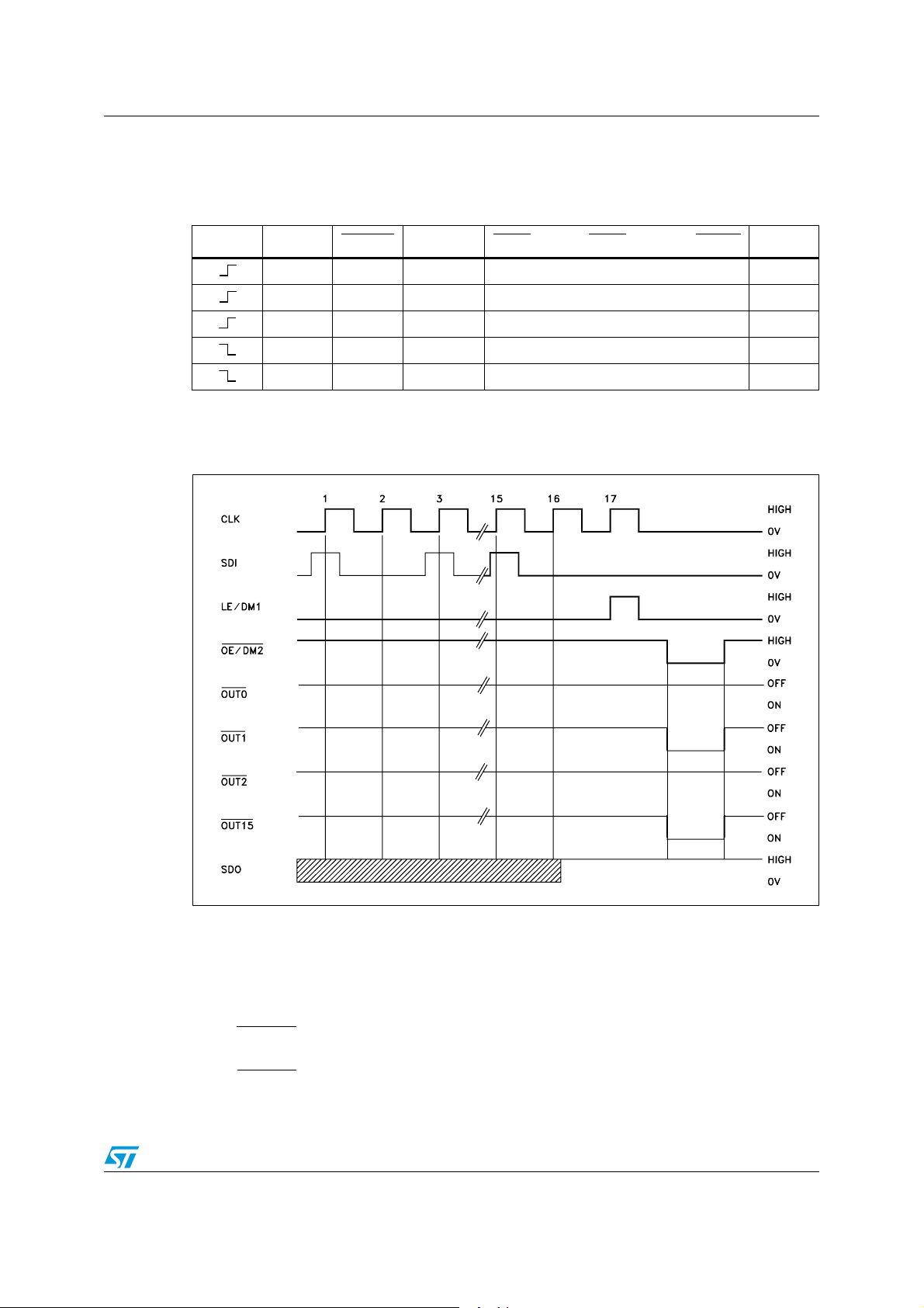
Table 9. Truth table
CLOCK LE/DM1 OE/DM2 SERIAL-IN OUT0 ............. OUT7 ................ OUT15 SDO
H L Dn Dn ..... Dn - 7 ..... Dn -15 Dn - 15
L L Dn + 1 No change Dn - 14
H L Dn + 2 Dn + 2 ..... Dn - 5 ..... Dn -13 Dn - 13
X L Dn + 3 Dn + 2 ..... Dn - 5 ..... Dn -13 Dn - 13
X H Dn + 3 OFF Dn - 13
Note: OUTn = ON when Dn = H OUTn = OFF when Dn = L
Figure 7. Timing diagram
Note: 1 Latch and output enable terminals are level-sensitive and are not synchronized with rising or
falling edge of CLK signal.
2 When LE/DM1 terminal is low level, the latch circuit holds previous set of data.
3 When LE/DM1 terminal is high level, the latch circuit refreshes new set of data from SDI
chain.
4 When OE/DM2
terminal is at low level, the output terminals Out 0 to Out 15 respond to data
in the latch circuits, either ‘1’ for ON or ‘0’ for OFF.
5 When OE/DM2
terminal is at high level, all output terminals are switched OFF.
Doc ID 16518 Rev 1 11/32
Page 12
Timing diagrams STP16DPP05
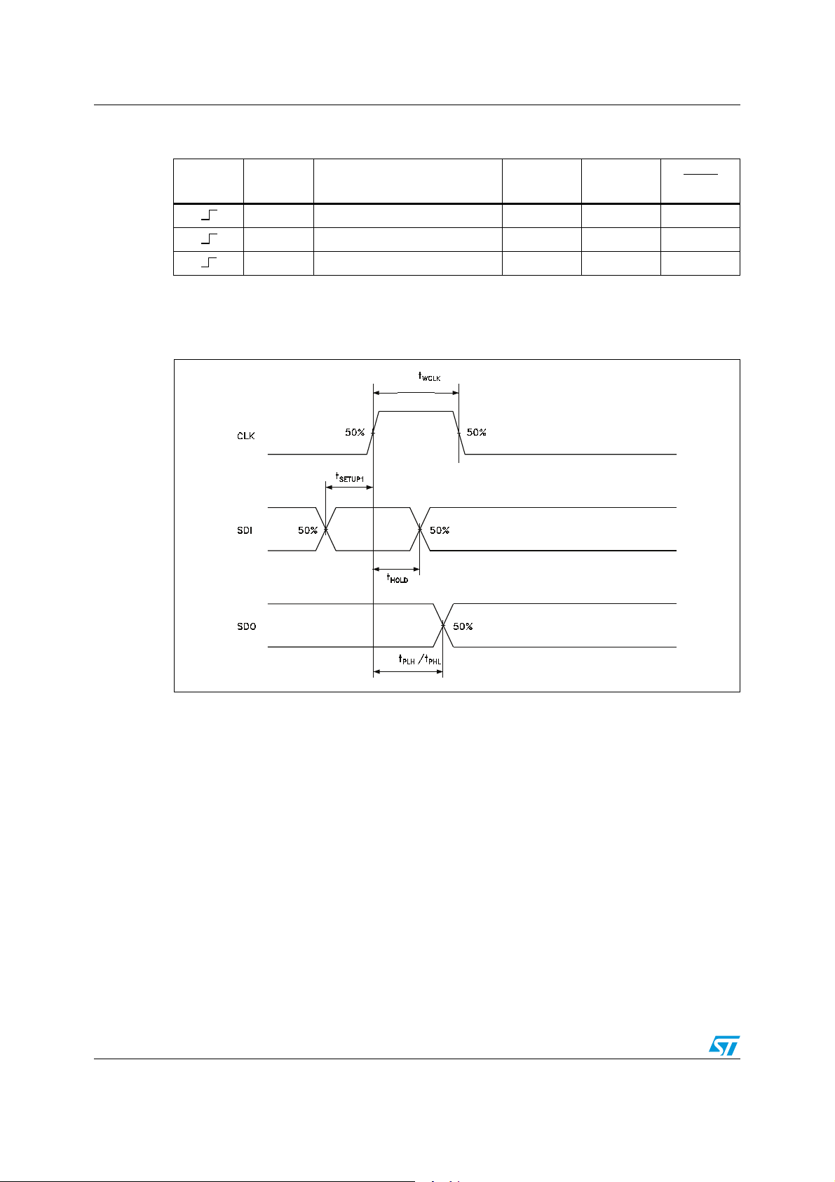
Table 10. Enable IO: shutdown truth table
CLOCK LE/DM1 SDI0 ........... SDI7 ............ SDI
H All = L Active Not active
L No change No change No change No change
H One or more = H Not active Active X
1. At power-up, the device starts in shutdown mode.
2. Undefined.
Figure 8. Clock, serial-in, serial-out
15
SH
Auto
Power-up
(1)
OUTn
OFF
(2)
12/32 Doc ID 16518 Rev 1
Page 13
STP16DPP05 Timing diagrams
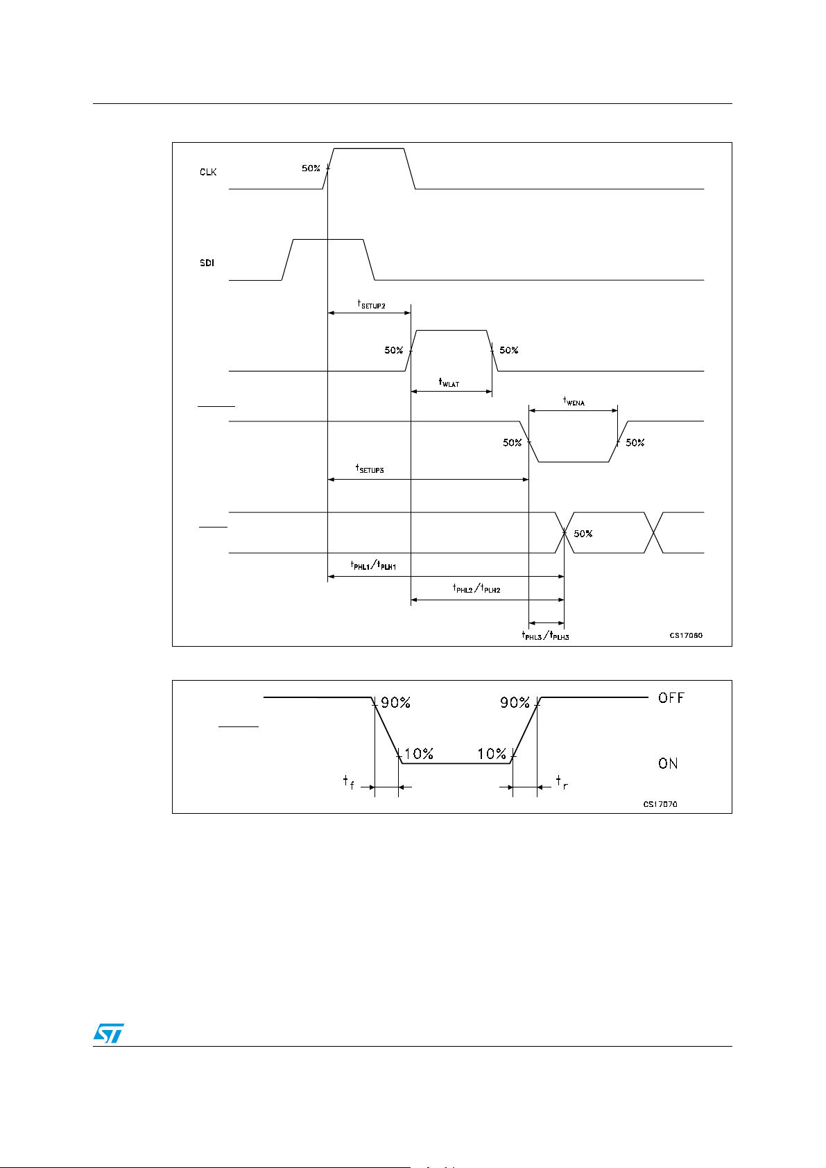
Figure 9. Clock, serial-in, latch, enable, outputs
LE/DM1
OE/DM2
OUTn
Figure 10. Outputs
OUTn
Doc ID 16518 Rev 1 13/32
Page 14
Typical characteristics STP16DPP05
6 Typical characteristics
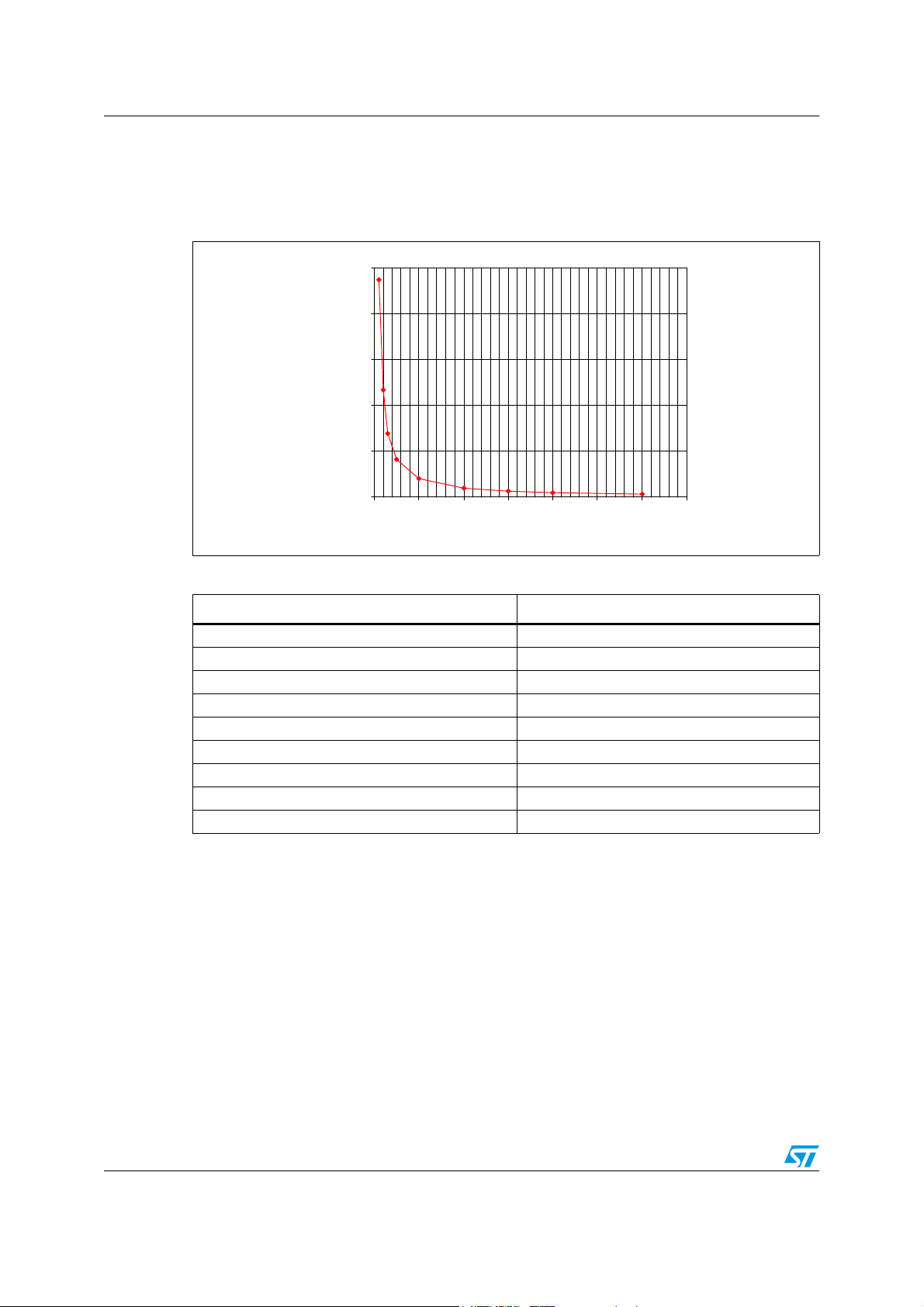
Figure 11. Output current vs. R-EXT resistor
25000
20000
15000
10000
R external (O hm)
5000
0
0 1020304050 6070
Current (mA)
Table 11. Output current vs. R-EXT resistor
R-EXT (Ω) Output current (mA)
23700 1
11730 2
6930 3
4090 5
2025 10
1000 20
667 30
497 40
331 60
14/32 Doc ID 16518 Rev 1
Page 15
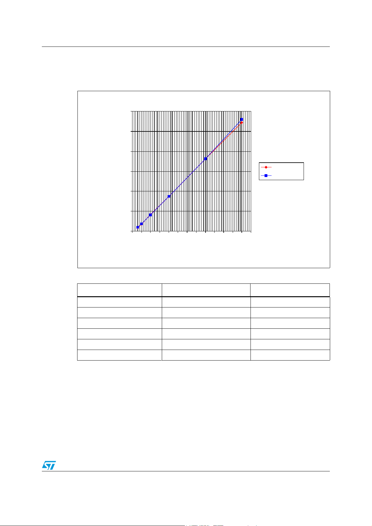
STP16DPP05 Typical characteristics
)
Conditions:
Temperature = 25 °C, V
= 3.3 V; 5.0 V, I
DD
= 3 mA; 5 mA; 10 mA; 20 mA; 50 mA; 60 mA.
SET
Figure 12. I
vs. dropout voltage (V
SET
drop
)
1200
1000
800
600
400
Min Drop Voltage (mV
200
0
0 5 10 15 20 25 30 35 40 45 50 55 60 65
Current (mA)
Avg @ 3.3V
Avg @ 5.0V
Table 12. I
vs. dropout voltage (V
SET
drop
)
Iout (mA) Avg (mV) @ 3.3 V Avg (mV)@ 5.0 V
33637
57172
10 163 163
20 346 347
40 724 726
60 1080 1110
Doc ID 16518 Rev 1 15/32
Page 16
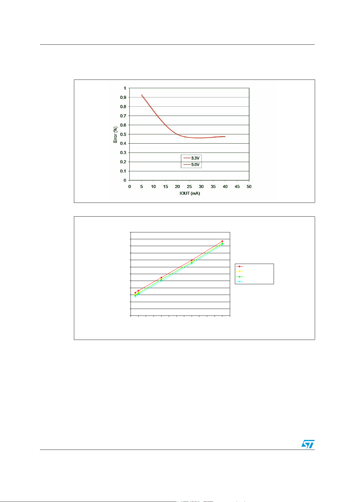
Typical characteristics STP16DPP05
TA = 25 °C, Vdd = 3.3 V; 5 V
Figure 13. Output current vs. ± ΔI
Figure 14. Idd ON/OFF
12
11
10
9
8
7
6
Idd (mA)
5
4
3
2
1
0
0 5 10 15 20 25 30 35 40 45 50 55 60 65
(%)
OL
Iset (mA)
AVG IDD ON @ 5.0 V
AVG IDD ON @ 3.3 V
AVG IDD OFF @ 5.0V
AVG IDD OFF @ 3.3V
16/32 Doc ID 16518 Rev 1
Page 17
STP16DPP05 Typical characteristics
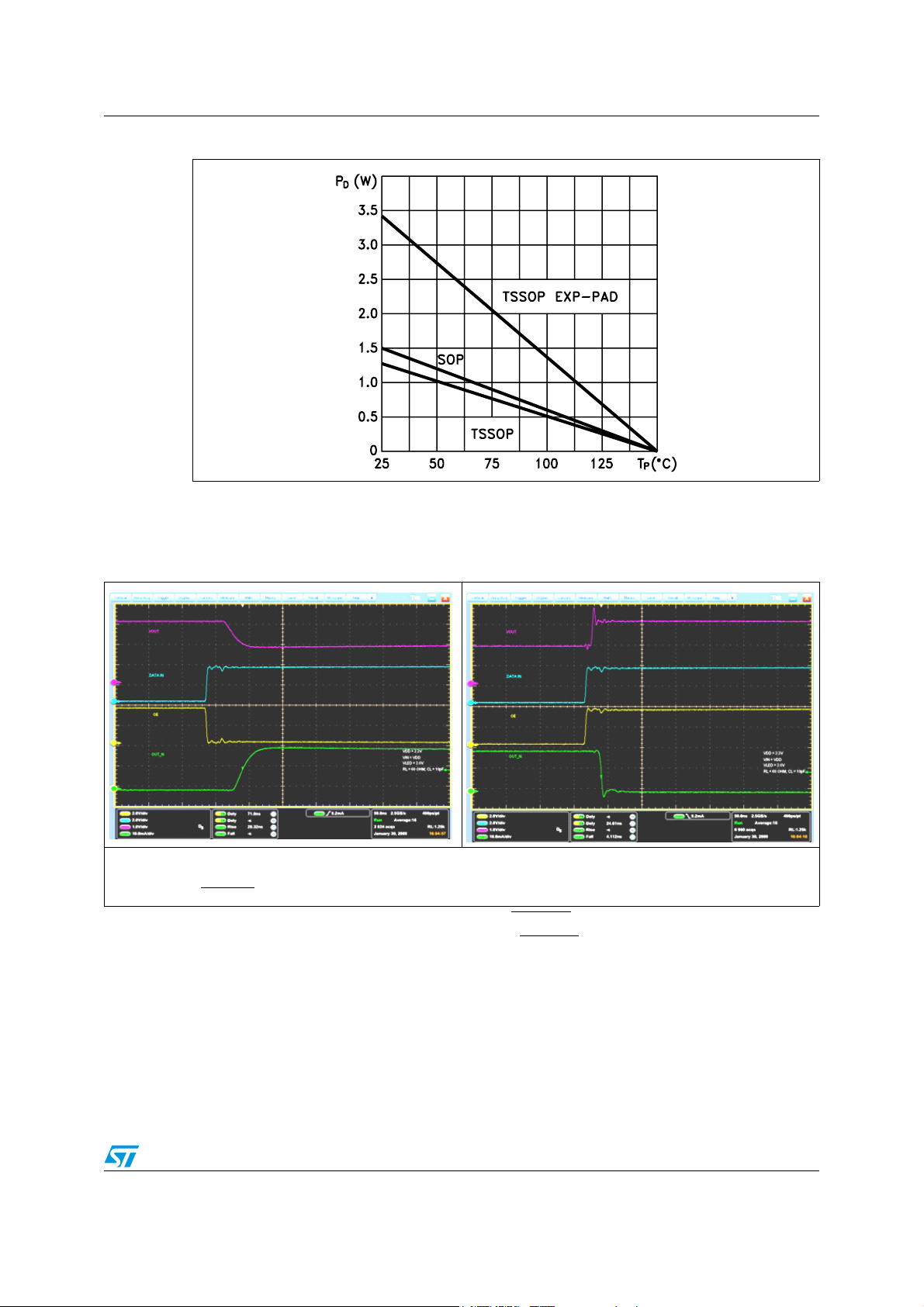
Figure 15. Power dissipation vs. package temperature
Note: The exposed pad should be soldered to the PCB to obtain the thermal benefits.
Figure 16. Turn ON output current
characteristics
(1)
Figure 17. Turn OFF output current
characteristics
(2)
Electrical conditions:
Vdd = 3.3 V, Vin = Vdd, Vled = 3.0 V, RL = 60 Ω, CL = 10 pF
Ch1 (Yellow) = OE/DM2
, Ch2 (Blue) = SDI, Ch3 (Purple) = VOUT, Ch4 (Green) = OUT
1. The reference level for the TON characteristics is 50% of OE/DM2 signal and 90% of output current
2. The reference level for the T
current
characteristics is 50% of OE/DM2 signal and 10% of output
OFF
Doc ID 16518 Rev 1 17/32
Page 18
Error detection mode functionality STP16DPP05
7 Error detection mode functionality
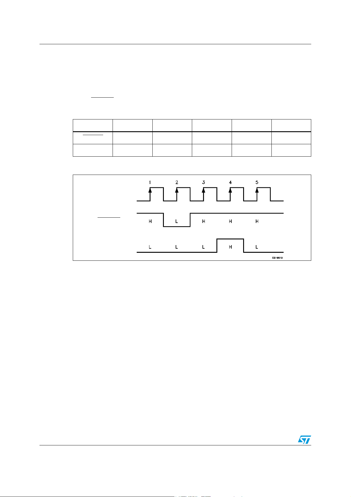
7.1 Phase one: entering error detection mode
From the “normal mode” condition the device can switch to “error mode” by a logic sequence
on the OE/DM2
Table 13. Entering error detection mode - truth table
CLK1°2°3°4°5°
and LE/DM1 pins, as shown in the following table and diagram:
OE/DM2
HLHHH
LE/DM1 LLLHL
Figure 18. Entering error detection mode - timing diagram
CLK
OE/DM2
LE/DM1
After these five CLK cycles, the device goes into “error detection mode” and at the rising
edge of the 6th CLK cycle, the SDI data are ready for sampling.
18/32 Doc ID 16518 Rev 1
Page 19
STP16DPP05 Error detection mode functionality
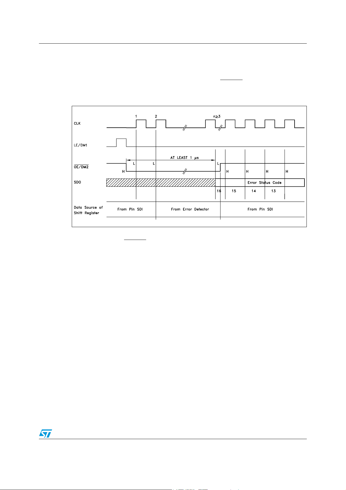
7.2 Phase two: error detection
The 16 data bits must be set to “1” in order for all the outputs to be ON during error
detection. The data are latched by LE/DM1, after which the outputs are ready for the
detection process. When the microcontroller switches the OE/DM2
drives the LEDs to analyze if an OPEN or SHORT condition has occurred.
Figure 19. Detection diagram
to LOW, the device
The status of the LEDs is detected in at least 1 microsecond, and after this period the
microcontroller sets OE/DM2
to HIGH state and the output data detection result is sent to
the microcontroller via SDO.
Error detection mode and normal mode both use the same data format. As soon as all the
detection data bits are available on the serial line, the device may return to normal mode of
operation. To re-detect the status, the device must first return to normal mode and reenter
error detection mode.
Doc ID 16518 Rev 1 19/32
Page 20
Error detection mode functionality STP16DPP05
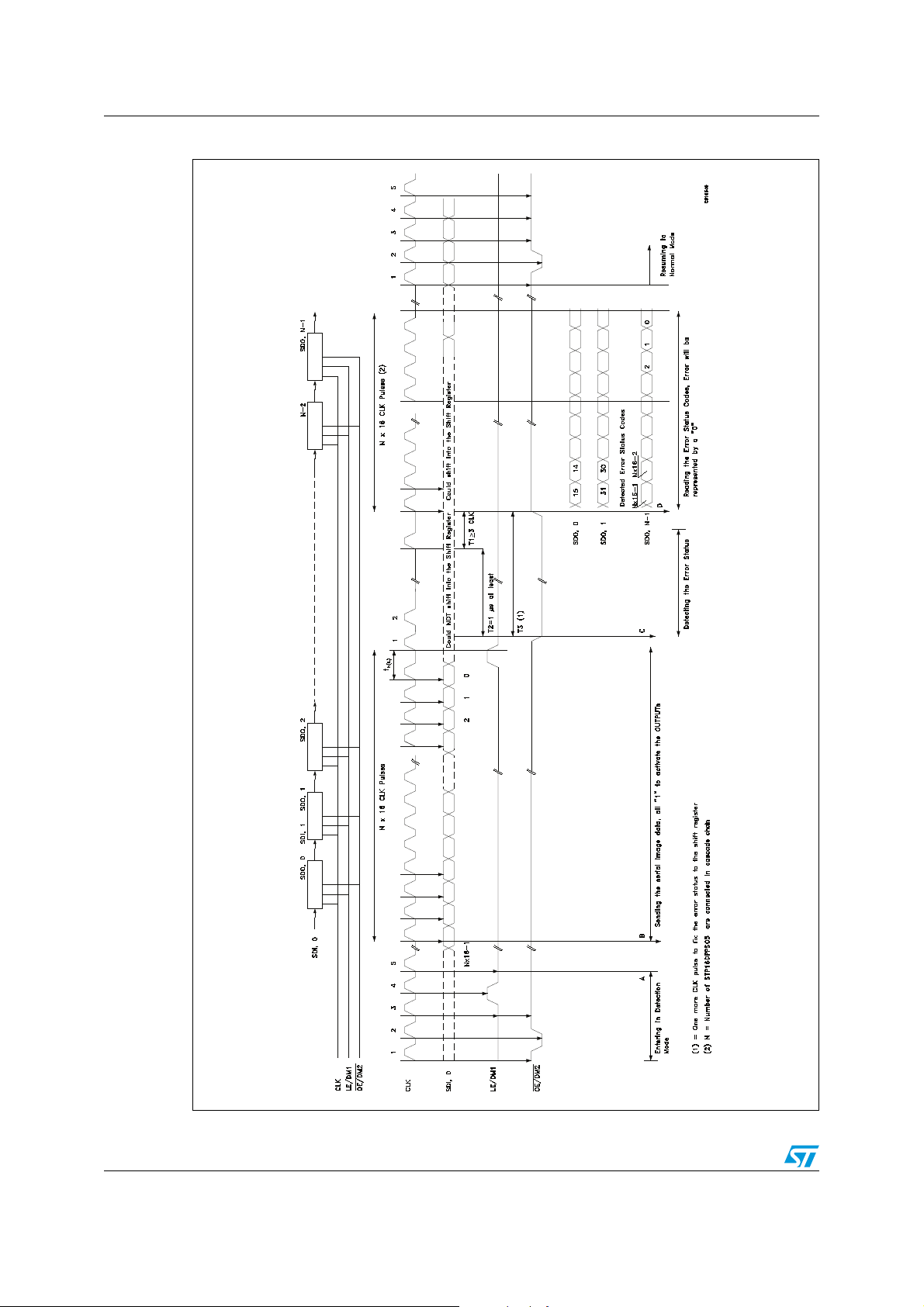
Figure 20. Timing example for open and/or short-circuit detection
D.U.T. D. U.T. D.U.T. D.U. T. D. U.T.
20/32 Doc ID 16518 Rev 1
Page 21
STP16DPP05 Error detection mode functionality
7.3 Phase three: resuming normal mode
The sequence for reentering normal mode is shown in the following table:
Figure 21. Resuming normal mode - timing diagram
CLK1°2°3°4°5°
OE/DM2
HLHHH
LE/DM1 LLLLL
Note: For proper device operation, the “entering error detection” sequence must be followed by a
“resume mode” sequence, it is not possible to insert consecutive equal sequences.
7.4 Error detection conditions
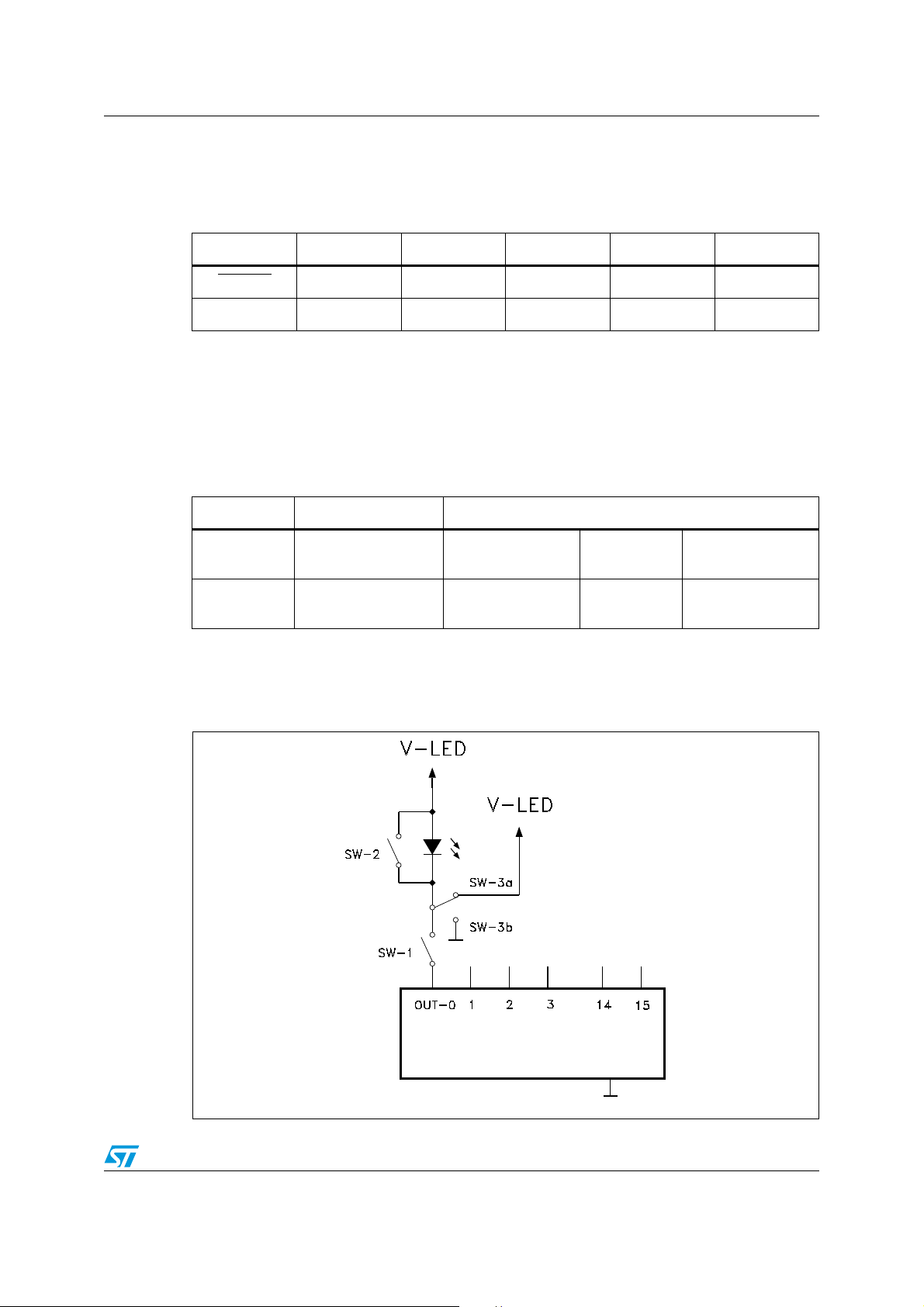
Table 14. Detection conditions (VDD = 3.3 to 5 V, temperature range -40 to 125 °C)
Configuration Detect mode Detection results
SW-1 or
SW-3b
SW-2 or
SW-3a
Note: Where: IO = the output current programmed by the R-EXT, I
current in detection mode
Figure 22. Detection circuit
Open line or output
short to GND detected
Short on LED or short
to V-LED detected
==> I
ODEC
≤ 0.5 x I
==> VO ≥ 2.6 V
No error
O
detected
No error
detected
==> I
==> VO ≤ 2.3 V
= the detected output
ODEC
ODEC
≥ 0.5 x I
O
STP16DPP05
16
Doc ID 16518 Rev 1 21/32
Page 22
Error detection mode functionality STP16DPP05
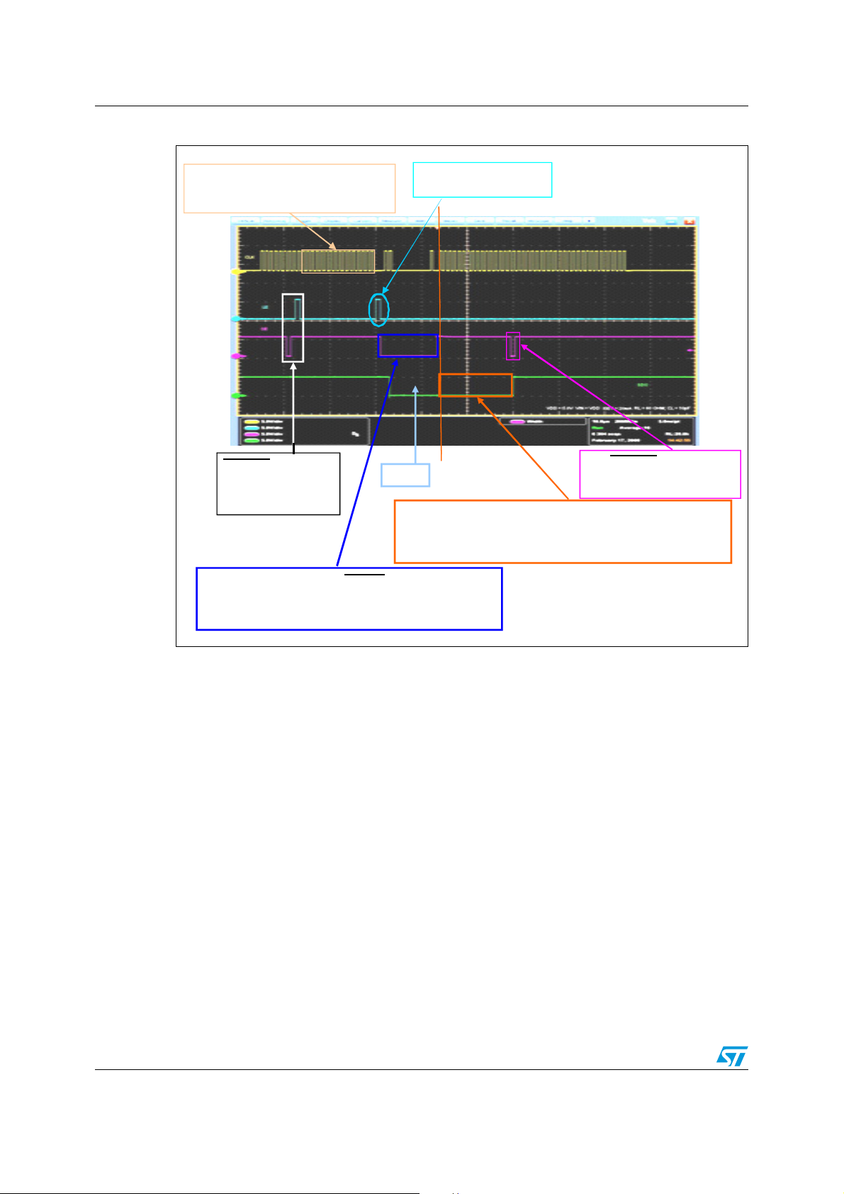
Figure 23. Error detection sequence
Feeding 16 b it of CLK signal af ter
entering the E DM, t he SD I s ig nal, s et to
This LE/DM1 pulse latch
the data to the outputs
1, is loaded in the shift register
OE/DM2 and LE/DM1
seq uence sig nals to
Igno re
start the error
detection sequence
On the rising edge of first CLK pulse after the detection, the SDO
pro vides the Out put s tat us f eedbac k with the s equence Out 15;
Out 14…Out 0.
In this case all t he outp uts are in f ault cond it io n (Open or Sho rt)
Turn ON t he outp ut with the OE/DM2 p in and wait 1 µs to
have the c o rrect out put s tat us acq uisition. D uring this time
a minimum of three CLK pulses are required (2 at the
beg inning and 1 at the end) to rewrite the shif t register.
This OE/DM2 pulse put the
device in Normal Mode
Cond itio n af ter EDM test
22/32 Doc ID 16518 Rev 1
Page 23
STP16DPP05 Package mechanical data
8 Package mechanical data
In order to meet environmental requirements, ST offers these devices in different grades of
ECOPACK
specifications, grade definitions and product status are available at: www.st.com.
ECOPACK
®
packages, depending on their level of environmental compliance. ECOPACK®
®
is an ST trademark.
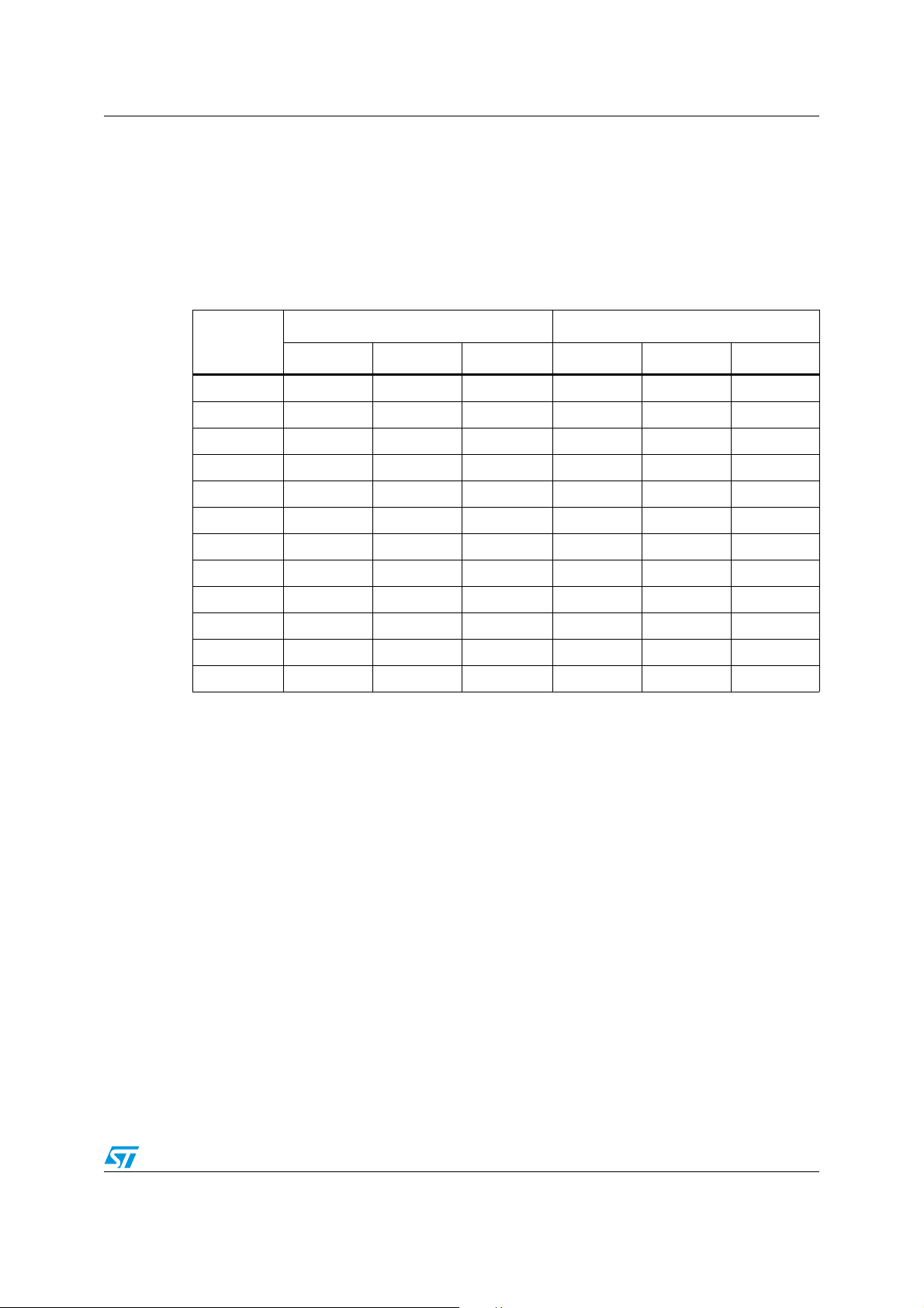
Table 15. QSOP-24 mechanical data
mm. inch
Dim.
Min Typ Max Min Typ Max
A 1.54 1.62 1.73 0.061 0.064 0.068
A1 0.1 0.15 0.25 0.004 0.006 0.010
A2 1.47 0.058
b 0.31 0.2 0.012 0.008
c 0.254 0.17 0.010 0.007
D 8.56 8.66 8.76 0.337 0.341 0.345
E 5.8 6 6.2 0.228 0.236 0.244
E1 3.8 3.91 4.01 0.150 0.154 0.158
e 0.635 0.025
L 0.4 0.635 0.89 0.016 0.025 0.035
h 0.25 0.33 0.41 0.010 0.013 0.016
< 8° 0°
Doc ID 16518 Rev 1 23/32
Page 24
Package mechanical data STP16DPP05
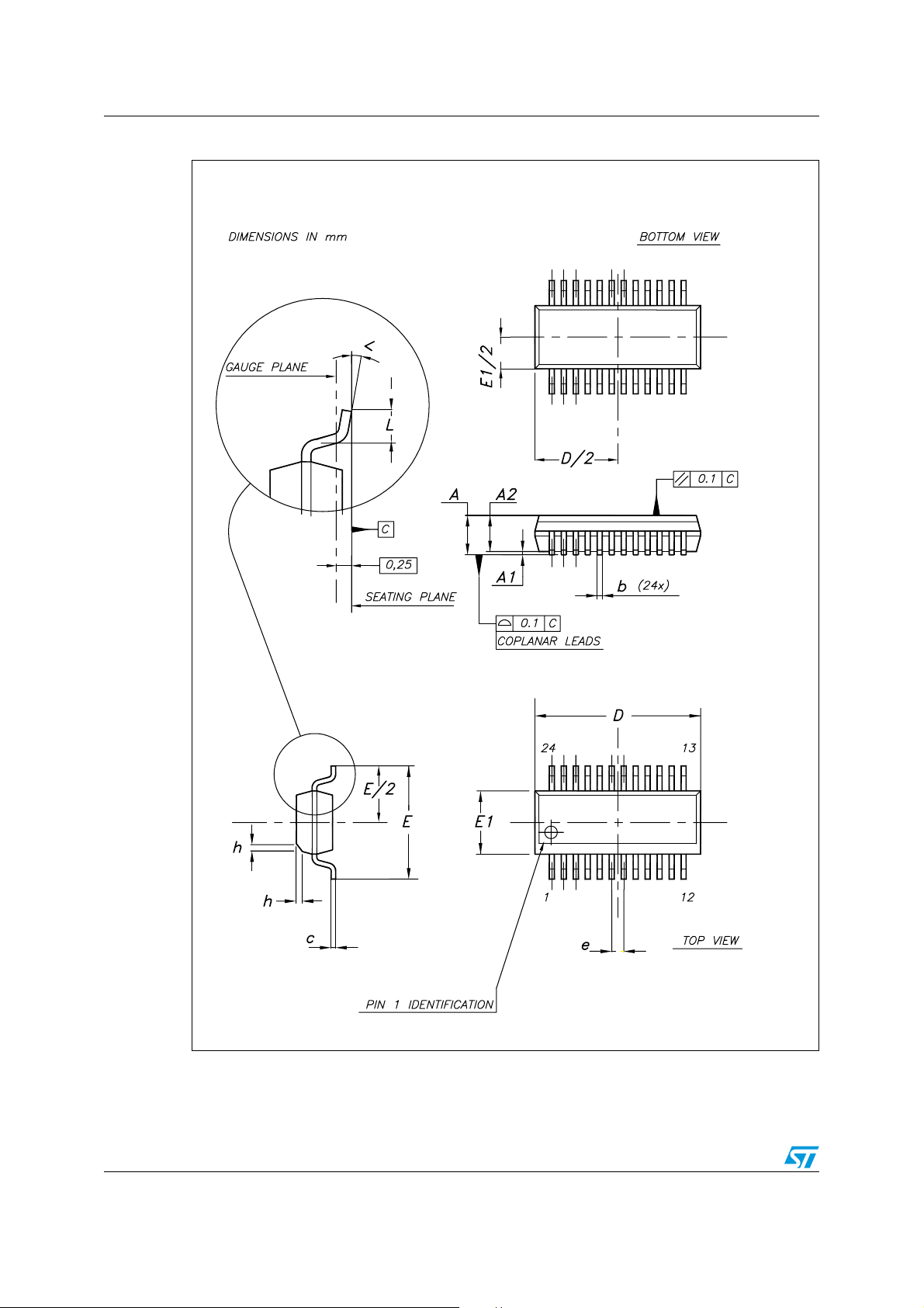
Figure 24. QSOP-24 package dimensions
24/32 Doc ID 16518 Rev 1
Page 25
STP16DPP05 Package mechanical data
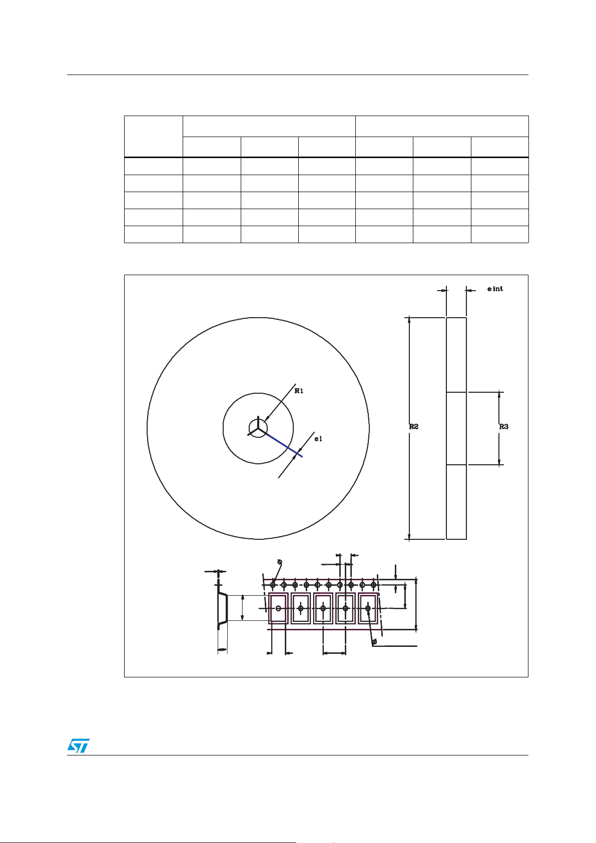
Table 16. QSOP-24 tape and reel
mm. Inches
Dim.
Min Typ Max Min Typ Max
R1 12.8 13 13.5 5.039 5.118 5.315
R2 330 129.921
R3 100 39.37
eint 16.4 6.457
e1 1.5 2 2.5 0.591 0.787 0.984
Figure 25. QSOP-24 tape and reel dimensions
4.0+/-0.1
4.0+/-0.1
2.0+/-0.1
1.5+1/0
0.3+/-0.05
0.3+/-0.05
1
1
0
0
.
.
3
3
+
+
/
/
-
0
0
.
.
1
1
2.1 +/-0.1
2.1 +/-0.1
1.5+1/0
6
6
.
.
5
5
+
+
/
/
-
-
0
0
.
.
2.0+/-0.1
8 +/-0.1
8 +/-0.1
1
1
1.75+/-0.1
1.75+/-0.1
7.5+/-0.1
7.5+/-0.1
1.6 +1/-0.1
1.6 +1/-0.1
16 +/-0.3
16 +/-0.3
7217811_C
Doc ID 16518 Rev 1 25/32
Page 26
Package mechanical data STP16DPP05
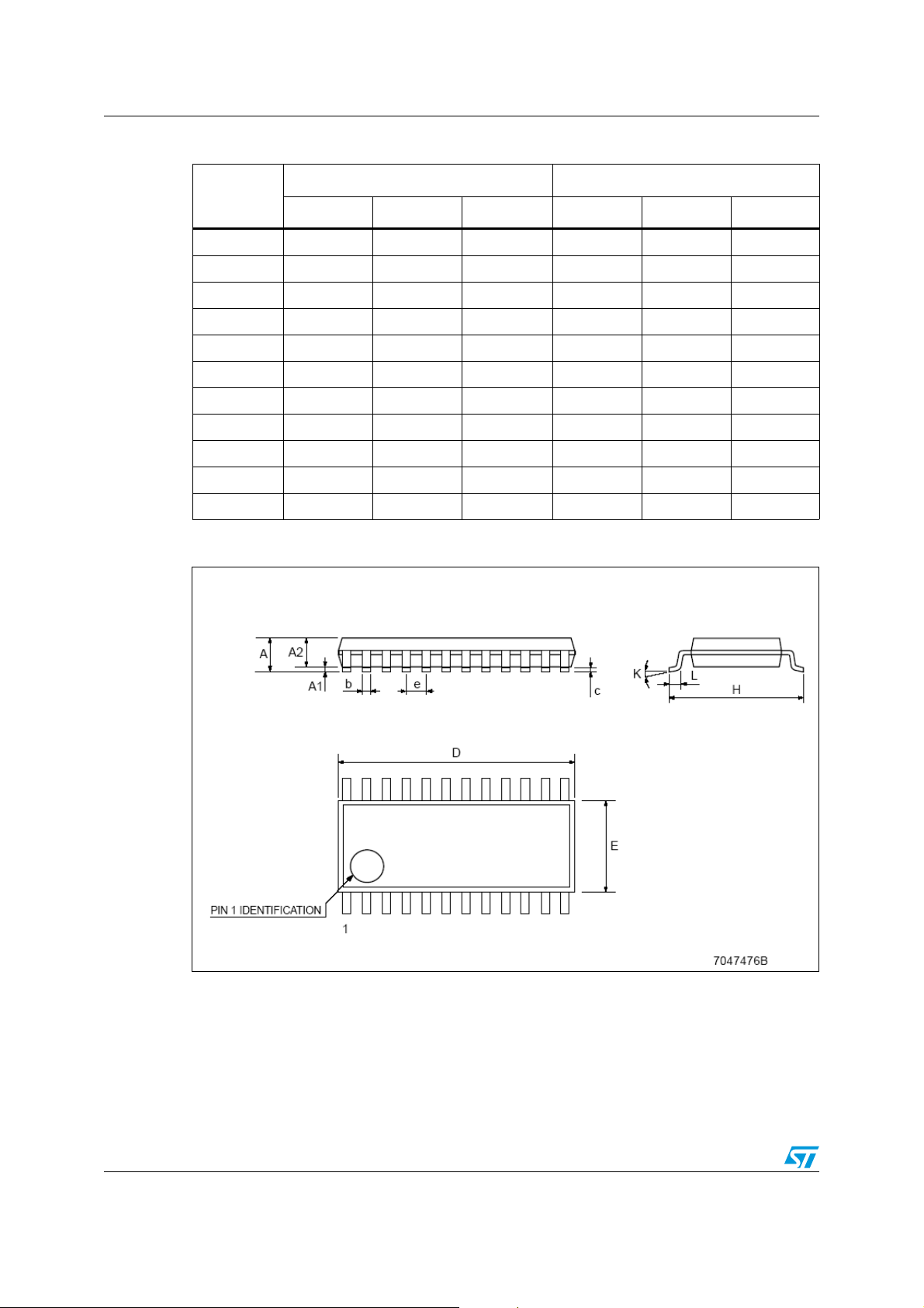
Table 17. TSSOP24 mechanical data
mm. Inches
Dim.
Min Typ Max Min Typ Max
A 1.1 0.043
A1 0.05 0.15 0.002 0.006
A2 0.9 0.035
b 0.19 0.30 0.0075 0.0118
c 0.09 0.20 0.0035 0.0079
D 7.7 7.9 0.303 0.311
E 4.3 4.5 0.169 0.177
e 0.65 BSC 0.0256 BSC
H 6.25 6.5 0.246 0.256
K 0° 8° 0° 8°
L 0.50 0.70 0.020 0.028
Figure 26. TSSOP24 package dimensions
26/32 Doc ID 16518 Rev 1
Page 27
STP16DPP05 Package mechanical data
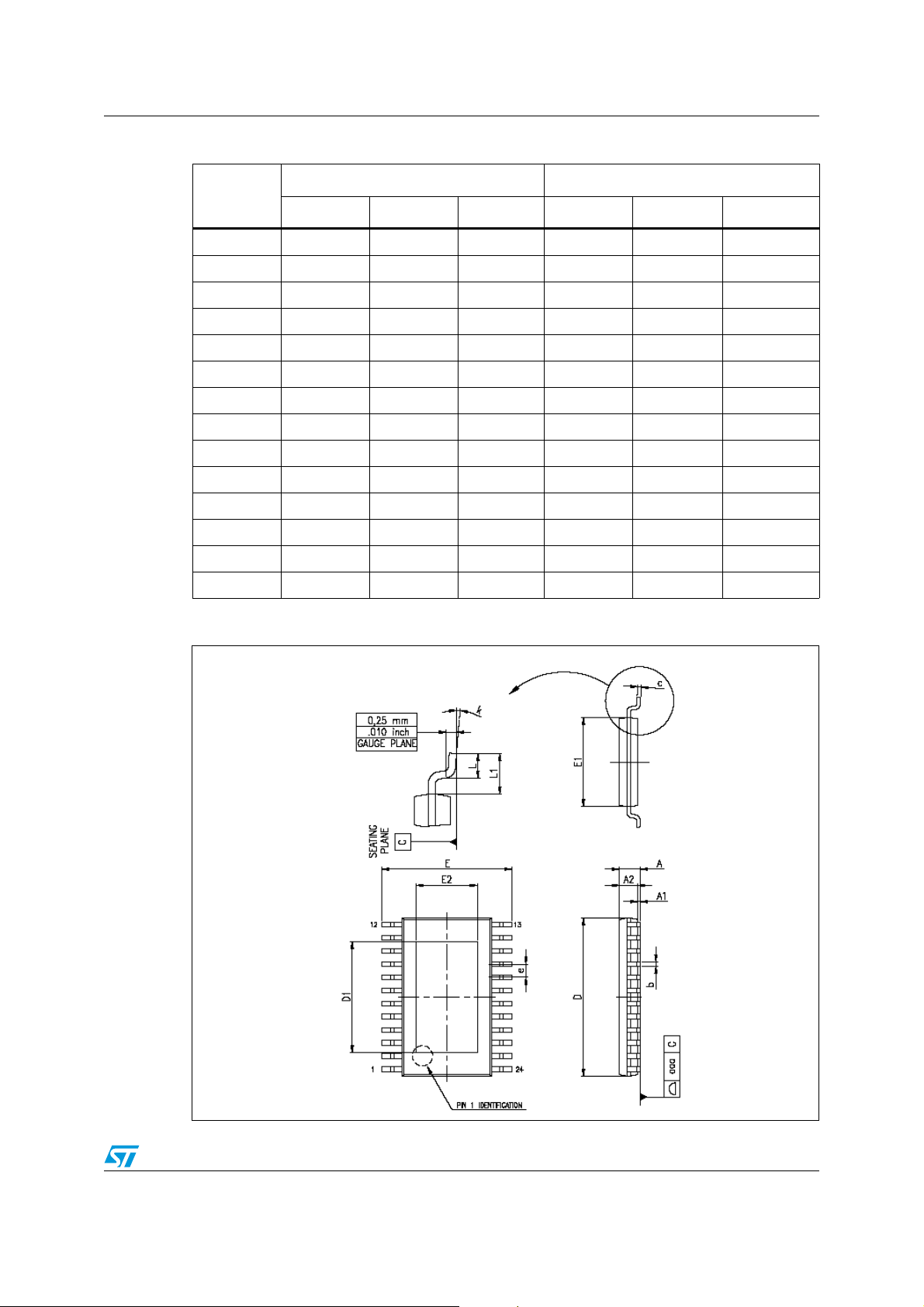
Table 18. TSSOP24 exposed pad mechanical data
mm Inches
Dim.
Min Typ Max Min Typ Max
A 1.2 0.047
A1 0.15 0.004 0.006
A2 0.8 1 1.05 0.031 0.039 0.041
b 0.19 0.30 0.007 0.012
c 0.09 0.20 0.004 0.0089
D 7.7 7.8 7.9 0.303 0.307 0.311
D1 4.7 5.0 5.3 0.185 0.197 0.209
E 6.2 6.4 6.6 0.244 0.252 0.260
E1 4.3 4.4 4.5 0.169 0.173 0.177
E2 2.9 3.2 3.5 0.114 0.126 0.138
e 0.65 0.0256
K 0° 8° 0° 8°
L 0.45 0.60 0.75 0.018 0.024 0.030
Figure 27. TSSOP24 exposed pad dimensions
Doc ID 16518 Rev 1 27/32
Page 28
Package mechanical data STP16DPP05
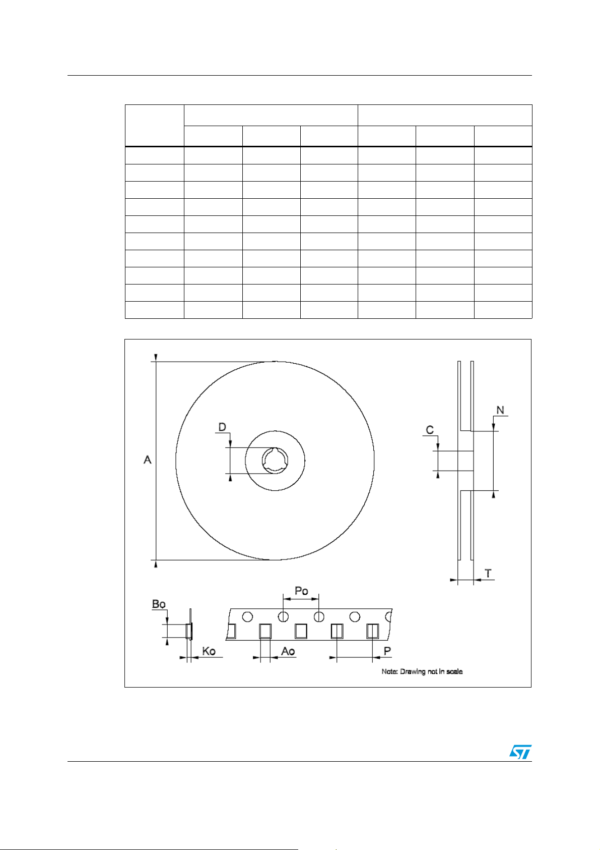
Table 19. Tape and reel TSSOP24 and TSSOP24 exposed pad
mm. Inches
Dim.
Min Typ Max Min Typ Max
A 330 12.992
C 12.8 13.2 0.504 0.519
D 20.2 0.795
N 60 2.362
T 22.4 0.882
Ao 6.8 7 0.268 0.276
Bo 8.2 8.4 0.323 0.331
Ko 1.7 1.9 0.067 0.075
Po 3.9 4.1 0.153 0.161
P 11.9 12.1 0.468 0.476
Figure 28. TSSOP24 and TSSOP24 exposed pad tape and reel dimensions
28/32 Doc ID 16518 Rev 1
Page 29
STP16DPP05 Package mechanical data
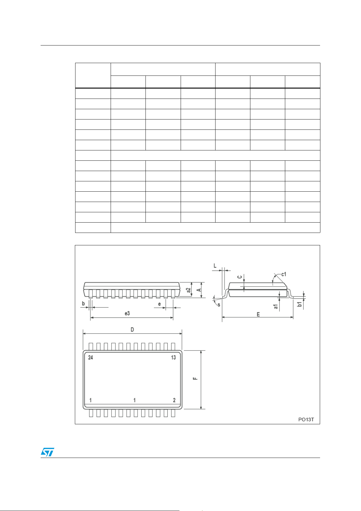
Table 20. SO-24 mechanical data
mm. Inches
Dim.
Min Typ Max Min Typ Max
A 2.65 0.104
a1 0.1 0.2 0.004 0.008
a2 2.45 0.096
b 0.35 0.49 0.014 0.019
b1 0.23 0.32 0.009 0.012
C 0.5 0.020
c1 45°(typ.)
D 15.20 15.60 0.598 0.614
E 10.00 10.65 0.393 0.419
e 1.27 0.050
e3 13.97 0.550
F 7.40 7.60 0.291 0.300
L 0.50 1.27 0.020 0.050
S °(max.) 8
Figure 29. SO-24 package dimensions
Doc ID 16518 Rev 1 29/32
Page 30
Package mechanical data STP16DPP05
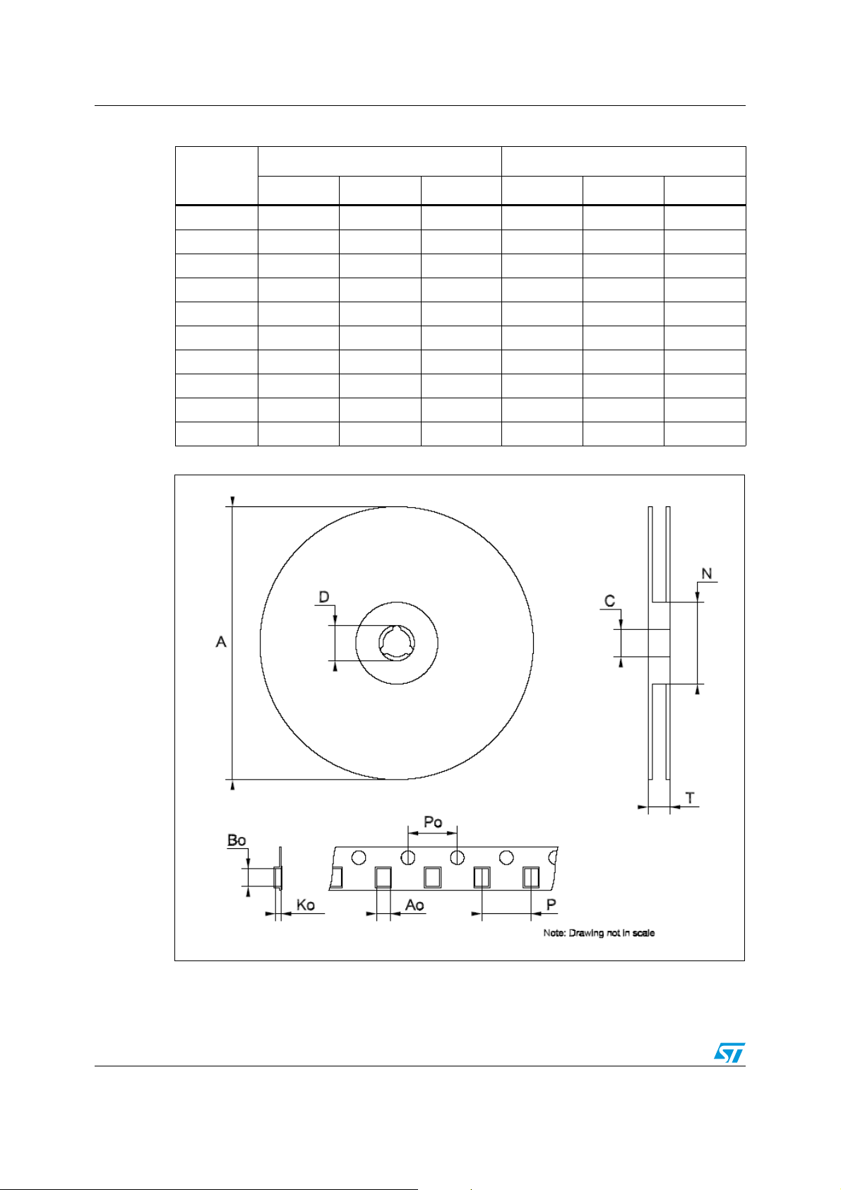
Table 21. Tape and reel SO-24
mm. Inches
Dim.
Min Typ Max Min Typ Max
A 330 12.992
C 12.8 13.2 0.504 0.519
D 20.2 0.795
N 60 2.362
T 30.4 1.197
Ao 10.8 11.0 0.425 0.433
Bo 15.7 15.9 0.618 0.626
Ko 2.9 3.1 0.114 0.122
Po 3.9 4.1 0.153 0.161
P 11.9 12.1 0.468 0.476
Figure 30. SO-24 tape and reel dimensions
30/32 Doc ID 16518 Rev 1
Page 31

STP16DPP05 Revision history
9 Revision history
Table 22. Document revision history
Date Revision Changes
22-Oct-2009 1 Initial release.
Doc ID 16518 Rev 1 31/32
Page 32

STP16DPP05
Please Read Carefully:
Information in this document is provided solely in connection with ST products. STMicroelectronics NV and its subsidiaries (“ST”) reserve the
right to make changes, corrections, modifications or improvements, to this document, and the products and services described herein at any
time, without notice.
All ST products are sold pursuant to ST’s terms and conditions of sale.
Purchasers are solely responsible for the choice, selection and use of the ST products and services described herein, and ST assumes no
liability whatsoever relating to the choice, selection or use of the ST products and services described herein.
No license, express or implied, by estoppel or otherwise, to any intellectual property rights is granted under this document. If any part of this
document refers to any third party products or services it shall not be deemed a license grant by ST for the use of such third party products
or services, or any intellectual property contained therein or considered as a warranty covering the use in any manner whatsoever of such
third party products or services or any intellectual property contained therein.
UNLESS OTHERWISE SET FORTH IN ST’S TERMS AND CONDITIONS OF SALE ST DISCLAIMS ANY EXPRESS OR IMPLIED
WARRANTY WITH RESPECT TO THE USE AND/OR SALE OF ST PRODUCTS INCLUDING WITHOUT LIMITATION IMPLIED
WARRANTIES OF MERCHANTABILITY, FITNESS FOR A PARTICULAR PURPOSE (AND THEIR EQUIVALENTS UNDER THE LAWS
OF ANY JURISDICTION), OR INFRINGEMENT OF ANY PATENT, COPYRIGHT OR OTHER INTELLECTUAL PROPERTY RIGHT.
UNLESS EXPRESSLY APPROVED IN WRITING BY AN AUTHORIZED ST REPRESENTATIVE, ST PRODUCTS ARE NOT
RECOMMENDED, AUTHORIZED OR WARRANTED FOR USE IN MILITARY, AIR CRAFT, SPACE, LIFE SAVING, OR LIFE SUSTAINING
APPLICATIONS, NOR IN PRODUCTS OR SYSTEMS WHERE FAILURE OR MALFUNCTION MAY RESULT IN PERSONAL INJURY,
DEATH, OR SEVERE PROPERTY OR ENVIRONMENTAL DAMAGE. ST PRODUCTS WHICH ARE NOT SPECIFIED AS "AUTOMOTIVE
GRADE" MAY ONLY BE USED IN AUTOMOTIVE APPLICATIONS AT USER’S OWN RISK.
Resale of ST products with provisions different from the statements and/or technical features set forth in this document shall immediately void
any warranty granted by ST for the ST product or service described herein and shall not create or extend in any manner whatsoever, any
liability of ST.
ST and the ST logo are trademarks or registered trademarks of ST in various countries.
Information in this document supersedes and replaces all information previously supplied.
The ST logo is a registered trademark of STMicroelectronics. All other names are the property of their respective owners.
© 2009 STMicroelectronics - All rights reserved
Australia - Belgium - Brazil - Canada - China - Czech Republic - Finland - France - Germany - Hong Kong - India - Israel - Italy - Japan -
STMicroelectronics group of companies
Malaysia - Malta - Morocco - Philippines - Singapore - Spain - Sweden - Switzerland - United Kingdom - United States of America
www.st.com
32/32 Doc ID 16518 Rev 1
 Loading...