

Page 1
1
3
1
3
查询STF12PF06供应商
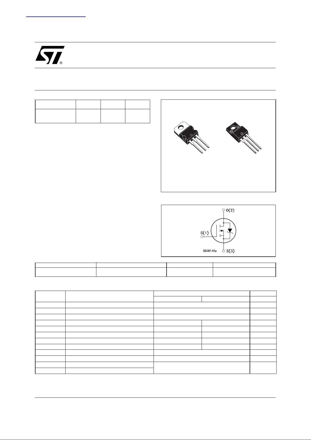
P-CHANNEL 60V - 0.18 Ω - 12A TO-220/TO-220FP
TYPE
STP12PF06
STF12PF06
■ TYPICAL R
■ EXCEPTIONAL dv/dt CAPABILITY
■ 100% AVALANCHE TESTED
■ LOW GATE CHARGE
■ APPLICATION ORIENTED
V
DSS
60 V
60 V
(on) = 0.18 Ω
DS
CHARACTERIZATION
DESCRIPTION
This Power MOSFET is the latest development of
STMicroelectronis unique "Single Feature Size™"
strip-based process. The resulting transistor
shows extremely high p acking density for low onresistance, rugged ava lanche characteristics and
less critical alignment steps therefore a
remarkable manufacturing reproducibility
R
DS(on)
< 0.20 Ω
< 0.20 Ω
I
D
12 A
12 A
STP12PF06
STF12PF06
STripFET™ II POWER MOSFET
Figure 1:PackageTable 1: General Features
2
TO-220 TO-220FP
Figure 2: Internal Schematic Diagram
2
APPLICATIONS
■ MOTOR CONTROL
■ DC-DC & DC-AC CONVERTERS
Table 2: Order Codes
PART NUMBER MARKING PACKAGE PACKAGING
STP12PF06
STF12PF06
P12PF06
F12PF06
TO-220
TO-220FP
TUBE
TUBE
Table 3: ABSOLUTE MAXIMUM RATINGS
Symbol Parameter Value Unit
STP20PF06 STF20PF06
V
DS
V
DGR
V
GS
I
D
I
D
I
(•)
DM
P
tot
dv/dt
E
AS
T
stg
T
j
(•) Pulse width limited by safe operating area.
:For the P-CHANNEL MOSFET actual polarity of voltages
NOTE
and current has to be reversed.
Drain-source Voltage (VGS = 0)
Drain-gate Voltage (RGS = 20 kΩ)
60 V
60 V
Gate- source Voltage ± 20 V
Drain Current (conti nuo us ) at TC = 25°C
Drain Current (conti nuo us ) at TC = 100°C
12 8 A
8.4 5.6 A
Drain Current (pulse d) 48 32 A
Total Dissipation at TC = 25°C
60 225 W
Derating Factor 0.4 0.17 W/°C
(1)
Peak Diode Recove ry vo ltag e slo pe 6 V/ns
(2)
Single Pulse Avalanche Energy 200 mJ
Storage Temperature
Operating Junction Temperature
(1) I
≤12A, di/dt ≤200A/µs, VDD ≤ V
SD
(2) Starting Tj = 25 oC, ID = 12A, VDD= 25V
-55 to 175 °C
(BR)DSS
, Tj ≤ T
JMAX
Rev. 2.0
1/10March 2005
Page 2

STP12PF06 STF12PF06
Table 4: THERMAL DATA
TO-220 TO-220FP
Rthj-case Thermal Resistance Junction-case Max 2.5 5.35 °C/W
Rthj-amb
T
l
Thermal Resistance Junction-ambient
Maximum Lead Temperature For Soldering Purpose
Max 62.5
300
°C/W
°C
ELECTRICAL CHARACTERISTICS (T
= 25 °C UNLESS OTHERWISE SPECIFIED)
CASE
Table 5: OFF
Symbol Parameter Test Conditions Min. Typ. Max. Unit
I
V
(BR)DSS
Drain-source
= 250 µA, VGS = 0
D
60 V
Breakdown Voltage
= Max Rating
I
DSS
I
GSS
Table 6: ON
Zero Gate Voltage
Drain Current (V
Gate-body Leakage
Current (V
(*)
DS
= 0)
GS
= 0)
V
DS
= Max Rating TC = 125°C
V
DS
= ± 20V
V
GS
1
10
±100 nA
Symbol Parameter Test Conditions Min. Typ. Max. Unit
V
GS(th)
R
DS(on)
Gate Threshold Voltage
Static Drain-source On
V
= VGS ID = 250 µA
DS
V
= 10 V ID = 10 A
GS
23.44 V
0.18 0.20 Ω
Resistance
Table 7: DYNAMIC
Symbol Parameter Test Conditions Min. Typ. Max. Unit
(2)
g
fs
C
iss
C
oss
C
rss
Forward Transconductance
Input Capacitance
Output Capacitance
Reverse Transfer
Capacitance
V
15 V
V
DS =
DS
ID
= 25V f = 1 MHz VGS = 0
= 6 A
2.5 6 S
850
230
75
µA
µA
pF
pF
pF
2/10
Page 3
STP12PF06 STF12PF06
ELECTRICAL CHARACTERISTICS (continued)
Table 8: SWITCHING ON
Symbol Parameter Test Conditions Min. Typ. Max. Unit
V
t
d(on)
Q
Q
Q
t
r
g
gs
gd
Turn-on Delay Time
Rise Time
Total Ga te Char ge
Gate-Source Charg e
Gate-Drain Charge
Table 9: SWITCHING OFF
Symbol Parameter Test Conditions Min. Typ. Max. Unit
t
d(off)
t
f
Turn-off Delay Time
Fall Time
Table 10: SOURCE DRAIN DIODE
Symbol Parameter Test Conditions Min. Typ. Max. Unit
I
SD
I
SDM
V
SD
t
rr
Q
rr
I
RRM
(1 )
Pulse width limited by safe operating area.
(2)
Pulsed: Pulse duration = 300 µs , duty cycle 1.5 %.
Source-drain Curre nt
(1)
Source-drain Curre nt (pu lse d)
(2)
Forward On Voltage
Reverse Recovery Time
Reverse Recovery Charge
Reverse Recovery Current
= 30 V ID = 6 A
DD
=4.7 Ω VGS = 10 V
R
G
(Resistive Load, Figu re 19)
V
= 48 V ID= 12 A VGS= 10 V
DD
V
= 30 V ID = 6 A
DD
=4.7Ω, V
R
G
GS
= 10 V
(Resistive Load, Figu re 19)
I
= 12 A VGS = 0
SD
I
= 12 A di/dt = 100A/µs
SD
= 30 V Tj = 150°C
V
DD
(see test circuit, Figure 21)
20
40
16
4
6
40
10
100
260
5.2
21 nC
10
40
2.5 V
ns
ns
nC
nC
ns
ns
A
A
ns
nC
A
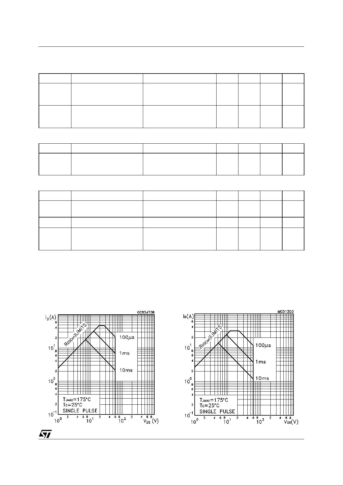
Figure 3: Safe Operating Area for TO-220 Figure 4: Safe Operating Area for TO-220FP
3/10
Page 4

STP12PF06 STF12PF06
Figure 5: Therm al Im pe da nce Figure 6: Thermal Impe da nce for TO -22 0F P
Figure 7: Output Characteristics Figure 8: Transf er Ch ar ac ter ist ics
Figure 9: Transconductance Figure 10: Static Drain-source On Resistance
4/10
Page 5

STP12PF06 STF12PF06
Figure 11: Gate Charge vs Gate-source Voltage Figure 12: Capacitance Variations
Figure 13: Normalized Gate Threshold Voltage vs
Temperature
Figure 15: Source-drain Diode Forward
Characteristics
Figure 14: Normalized on Resistan c e vs Te mpe r at ur e
Figure 16: Normalized Breakdown Voltage
Temperature
5/10
Page 6

STP12PF06 STF12PF06
Figure 17: Unclamped Inductive Load Test Circuit
Figure 19: Switching Times Test Circuits For Re-
sistive Load
Figure 18: Unclamped Inductive Waveform
Figure 20: Gate Charge test Circuit
Figure 21: Test Circuit For Inductive Load
Switching And Diode Recovery Times
6/10
Page 7

STP12PF06 STF12PF06
TO-220 MECHANICAL DATA
DIM.
A 4.4 4.6 0.173 0.181
C 1.23 1.32 0.048 0.051
D 2.40 2.72 0.094 0.107
E 0.49 0.70 0.019 0.027
F 0.61 0.88 0.024 0.034
F1 1.14 1.70 0.044 0.067
F2 1.14 1.70 0.044 0.067
G 4.95 5.15 0.194 0.203
G1 2.40 2.70 0.094 0.106
H2 10 10.40 0.393 0.409
L2 16.40 0.645
L3 28.90 1.137
L4 13 14 0.511 0.551
L5 2.65 2.95 0.104 0.116
L6 15.25 15.75 0.600 0.620
L7 6.20 6.60 0.244 0.260
L9 3.50 3.93 0.137 0.154
DIA 3.75 3.85 0.147 0.151
MIN. TYP. MAX. MIN. TYP. TYP.
mm. inch.
7/10
Page 8

STP12PF06 STF12PF06
TO-220FP MECHANICAL DAT A
DIM.
MIN. TYP. MAX. MIN. TYP. MAX.
A 4.4 4.6 0.173 0.181
B 2.5 2.7 0.098 0.106
D 2.5 2.75 0.098 0.108
E 0.45 0.7 0.017 0.027
F 0.75 1 0.030 0.039
F1 1.15 1.7 0.045 0.067
F2 1.15 1.7 0.045 0.067
G 4.95 5.2 0.195 0.204
G1 2.4 2.7 0.094 0.106
H 10 10.4 0.393 0.409
L2 16 0.630
L3 28.6 30.6 1.126 1.204
L4 9.8 10.6 0.385 0.417
L6 15.9 16.4 0.626 0.645
L7 9 9.3 0.354 0.366
Ø 3 3.2 0.118 0.126
mm inch
A
B
H
E
D
L3
L6
L7
¯
F1
F
G1
G
F2
123
L2
L4
8/10
Page 9

STP12PF06 STF12PF06
Table 11:Revision History
Date Revision Description of Changes
March 2005
March 2005
1.0 FIRST ISSUE
2.0 MINOR REVISION
9/10
Page 10

STP12PF06 STF12PF06
I
s
o
d
b
ct
t
ot
a
nformation furnished is believed to be accurate and reliable. However, STMicroelectronics assumes no responsibility for the consequence
f use of such information nor for any infrin gement of patents or other rights of third parties which may resul t from its use. No license is grant e
y implication or otherwise under any patent or patent rights of STMicroelectronics. Specifications mentioned in this publication are subje
o change without notic e. This publication supersedes and replaces all information previously supplied. ST Microelectronics products are n
uthorized for use as critical components in life support devices or systems without express written approval of STMicroelectronics.
The ST logo is registered trademark of STMicroelectronics
All other names are the property of their respective owners.
© 2005 STMicroelectronics - All Rights Reserved
Australia - Belgium - Brazil - Canada - China - Czech Republic - Finland - France - Germany - Hong Kong - India - Israel - Italy - Japan -
Malaysia - Malta - Morocco -Singapore - Spain - Sweden - Switzerland - United Kingdom - United States of Americ a.
STMicroelectronics group of comp anies
www.st.com
10/10
 Loading...