

Page 1
Feature summary
■ Meets the requirements of the universal serial
bus specification revision 2.0 And the on-thego supplement to the USB 2.0 specification
■ Analog car kit-compatible
■ Three operating modes: USB, UART and audio
■ Configurable using I
■ Capable of 12Mbit/s full-speed and 1.5Mbit/s
low-speed modes of operation
■ Standard digital interface compliant with the
OTG transceiver specification
■ Supports the session request protocol (SRP)
and host negotiation protocol (HNP)
■ 35mA Typical V
current for 3.3V supply voltage
■ Ability to control external charge pump for
higher V
■ Integrated pull-up/-down resistors
■ ±6kV ESD protection on all USB pins (contact
BUS
currents
discharge)
■ +1.6V to +3.6V Digital power supply and +2.7V
to +5.5V analog supply voltage range
■ Power-down mode with very low power
consumption for battery powered devices
■ Ideal for system ASICs with built-in USB OTG
dual role core
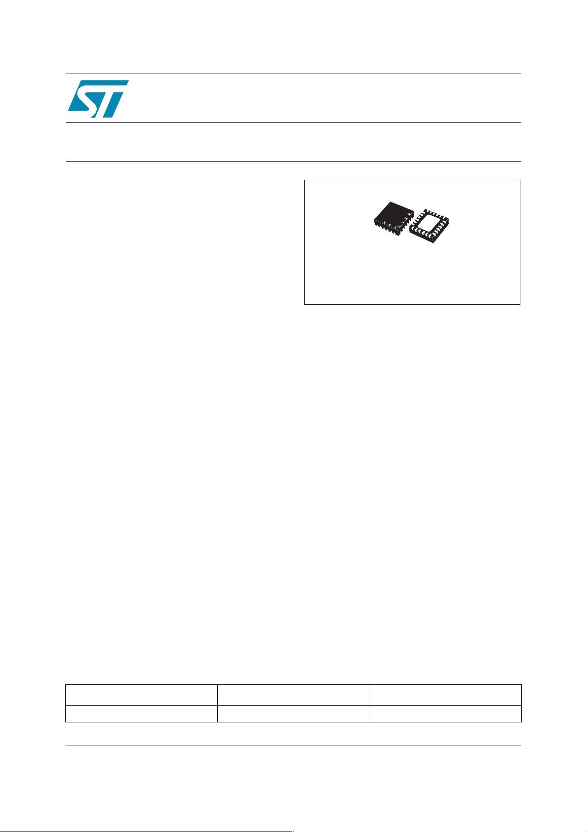
■ Available In QFN-24
■ –40°C to +85°C operating temperature range
2
C serial interface
Charge pump output
BUS
STOTG04ES
USB-OTG Full-speed Transceiver
QFN24 (4mmx4mm)
■ MP3 players
■ Digital cameras
■ Printers
Description
The STOTG04ES is a USB On-The-Go full-speed
transceiver. It provides complete physical layer
solution for any USB-OTG device. It contains
V
charge pump and comparators, ID line
BUS
detector and interrupt generator, and the USB
differential driver and receivers. The STOTG04
transceiver is suitable for mobile and battery
powered devices because of its low power
consumption and power down operating mode.
The transceiver is capable of operation in several
different modes. It can operate in basic USB-OTG
mode, as an UART transceiver or in audio mode.
Behavior of the transceiver is fully configurable
through the two-wire I
transceiver supports session request protocol and
host negotiation protocol.
2
C serial bus. The
Applications
■ Mobile phones
■ PDAs
Order code
Part number Package Packaging
STOTG04ESQTR QFN24 (4mm x 4mm) 4000 parts per reel
October 2006 Rev. 3 1/26
www.st.com
26
Page 2

Contents STOTG04ES
Contents
1 Pin configuration . . . . . . . . . . . . . . . . . . . . . . . . . . . . . . . . . . . . . . . . . . . . . 3
2 Maximum ratings . . . . . . . . . . . . . . . . . . . . . . . . . . . . . . . . . . . . . . . . . . . . . . 5
3 Electrical characteristics . . . . . . . . . . . . . . . . . . . . . . . . . . . . . . . . . . . . . . . 6
4 Charge pump characteristics . . . . . . . . . . . . . . . . . . . . . . . . . . . . . . . . . . 10
5 Timing diagrams . . . . . . . . . . . . . . . . . . . . . . . . . . . . . . . . . . . . . . . . . . . . . 11
6 Block description . . . . . . . . . . . . . . . . . . . . . . . . . . . . . . . . . . . . . . . . . . . . 14
6.1 Charge pump . . . . . . . . . . . . . . . . . . . . . . . . . . . . . . . . . . . . . . . . . . . . . . . . 14
6.2 V
6.3 Voltage regulator . . . . . . . . . . . . . . . . . . . . . . . . . . . . . . . . . . . . . . . . . . . . . . 14
6.4 ID Line detector . . . . . . . . . . . . . . . . . . . . . . . . . . . . . . . . . . . . . . . . . . . . . . . 14
6.5 Driver and receivers . . . . . . . . . . . . . . . . . . . . . . . . . . . . . . . . . . . . . . . . . . . 14
6.6 Control logic . . . . . . . . . . . . . . . . . . . . . . . . . . . . . . . . . . . . . . . . . . . . . . . . . 15
6.7 Modes of operation . . . . . . . . . . . . . . . . . . . . . . . . . . . . . . . . . . . . . . . . . . . . 15
6.8 Registers . . . . . . . . . . . . . . . . . . . . . . . . . . . . . . . . . . . . . . . . . . . . . . . . . . . . 17
6.9 I
6.10 Device address . . . . . . . . . . . . . . . . . . . . . . . . . . . . . . . . . . . . . . . . . . . . . . . 19
6.11 Bus protocol . . . . . . . . . . . . . . . . . . . . . . . . . . . . . . . . . . . . . . . . . . . . . . . . . 19
6.12 External charge pump switch . . . . . . . . . . . . . . . . . . . . . . . . . . . . . . . . . . . . 21
Comparators . . . . . . . . . . . . . . . . . . . . . . . . . . . . . . . . . . . . . . . . . . . . 14
BUS
6.7.1 Power modes . . . . . . . . . . . . . . . . . . . . . . . . . . . . . . . . . . . . . . . . . . . . . . . . . 15
6.7.2 USB Modes . . . . . . . . . . . . . . . . . . . . . . . . . . . . . . . . . . . . . . . . . . . . . . . . . . 15
6.7.3 UART Mode . . . . . . . . . . . . . . . . . . . . . . . . . . . . . . . . . . . . . . . . . . . . . . . . . . 16
6.7.4 Audio mode . . . . . . . . . . . . . . . . . . . . . . . . . . . . . . . . . . . . . . . . . . . . . . . . . . 17
2
C Bus interface . . . . . . . . . . . . . . . . . . . . . . . . . . . . . . . . . . . . . . . . . . . . . . 19
7 Package mechanical data . . . . . . . . . . . . . . . . . . . . . . . . . . . . . . . . . . . . . . 22
8 Revision history . . . . . . . . . . . . . . . . . . . . . . . . . . . . . . . . . . . . . . . . . . . . . . 25
2/26
Page 3
STOTG04ES Pin configuration
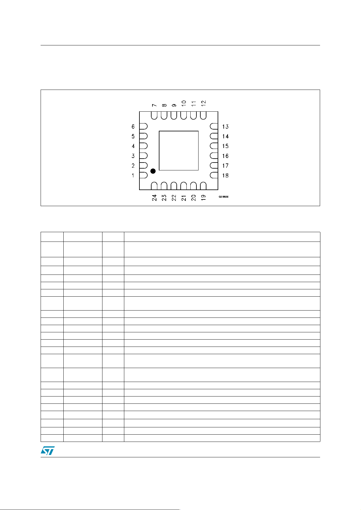
1 Pin configuration
Figure 1. Pin connections (bottom view )
Table 1. Pin description
PlN N° SYMBOL I/O NAME AND FUNCTION
2
1 ADR_PSW I/O
2 SDA I/O
3SCLI
4 RESET/ I Active low logic reset
5 INT/ O Active low interrupt signal (open-drain)
6 SPEED I Mode of the transceiver (0 = low-speed, 1 = full-speed) (2)
7
8 SUSPEND I Power down input (0 = active mode, 1 = power down) (See
9 OE_TP_INT/ I/O Output enable of the differential driver in the USB mode or interrupt output
10 VM O D– single-ended receiver output
11 VP O D+ single-ended receiver output
12 RCV O Differential receiver output
13 SE0_VM I/O
14 DAT_VP I/O
15 D- I/O Negative data line in the USB mode or serial data output in the UART mode
16 D+ I/O Positive data line in the USB mode or serial data input in the UART mode
17 GND Power Common analog and digital ground
18 ID I/O ID pin of the USB connector used for protocol identification
19
20
21 CAP1 I/O External capacitor pin for the charge pump
22 CAP2 I/O External capacitor pin for the charge pump
V
TRM
ExpPad - Not Connected
V
BUS
V
BAT
Power
Power Analog power supply voltage (+2.7V to +5.5V)
Least significant bit of the I
PSW output enabling or disabling an external charge pump
2
C serial data (1)
I
I2C clock
Internal voltage regulator output; an external decoupling capacitor should be
connected (3)
Single-ended zero input/output in the DAT_SE0 mode transmit mode, negative
data input/output in the single-ended transmit mode or TXD in the UART mode
Data input/output in the DAT_SE0 mode transmit mode, positive data input/
output in the single-ended transmit mode or RXD in the UART mode
line of the USB interface – it needs an external capacitor of 4.7µF
V
I/O
BUS
C address of the transceiver input latched on reset;
Ta bl e 8
)
3/26
Page 4
Pin configuration STOTG04ES
PlN N° SYMBOL I/O NAME AND FUNCTION
23 CGND Power Ground for the charge pump
24
(1) Input and open-drain output
(2) Input with internal pull-up resistor
(3) Internal regulator can be bypassed by connecting V
V
IF
Power Logic power supply (+1.6V to 3.6V)
to this pin when the V
BAT
is in range of 2.7V to 3.6V
BAT
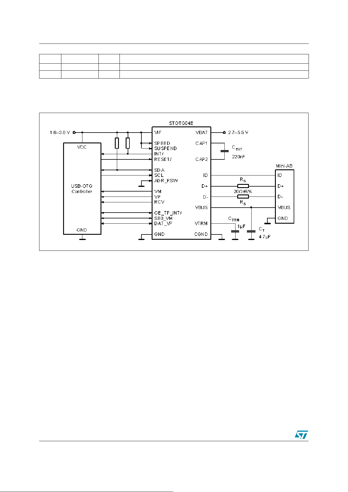
Figure 2. Functional diagram
4/26
Page 5
STOTG04ES Maximum ratings
2 Maximum ratings
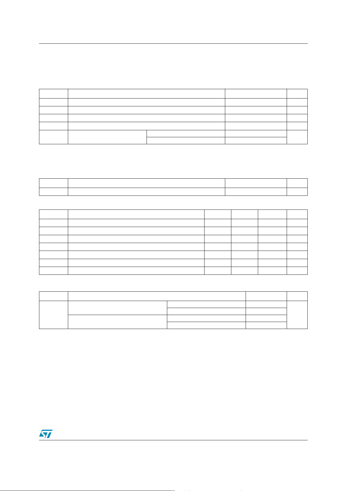
Table 2. Absolute maximum ratings
Symbol Parameter Value Unit
V
V
BAT
V
DCDIG
T
STG
V
ESD
(*) In accordance to IEC61000-4-2, level 3.
Absolute Maximum Ratings are those values beyond which damage to the device may occur. Functional Operation under these con-
ditions is not implied.
Table 3. Thermal data
Symbol Parameter Value Unit
R
thJA
Table 4. Recommended operating condition
Symbol Parameter Min. Typ. Max. Unit
V
V
BAT
T
C
EXT
C
C
TRM
R
Logic Supply Voltage -0.5 to + 4.5 V
IF
Analog Supply Voltage -0.5 to + 6.5 V
DC Input Voltage on any logic interface pin -0.5 to + 4.5 V
Storage Temperature Range -65 to + 150 °C
Electrostatic discharge voltage
on USB pins
Human Body Model ± 8
Contact Discharge (*) ± 6
Thermal Resistance Junction-Ambient 59 °C/W
Logic Supply Voltage 1.6 1.8 3.6 V
IF
Analog Supply Voltage 2.7 3.3 5.5 V
Operating Temperature Range -40 +85 °C
A
Charge pump external capacitor 100 220 470 nF
Charge pump tank capacitor 1 4.7 6.5 µF
T
Voltage regulator external capacitor 1 µF
Data lines impedance matching resistor 20 Ω
S
kV
Table 5. ESD Performance
Symbol Parameter Value Unit
IEC-61000-4-2 (D+, D-, VBUS, ID)
ESD
IEC-61000-4-2 (other pins)
Air discharge (10 pulses) ± 8
Contact discharge (10 pulses) ± 6
Air discharge (10 pulses) ± 2
Contact discharge (10 pulses) ± 2
kV
5/26
Page 6
Electrical characteristics STOTG04ES
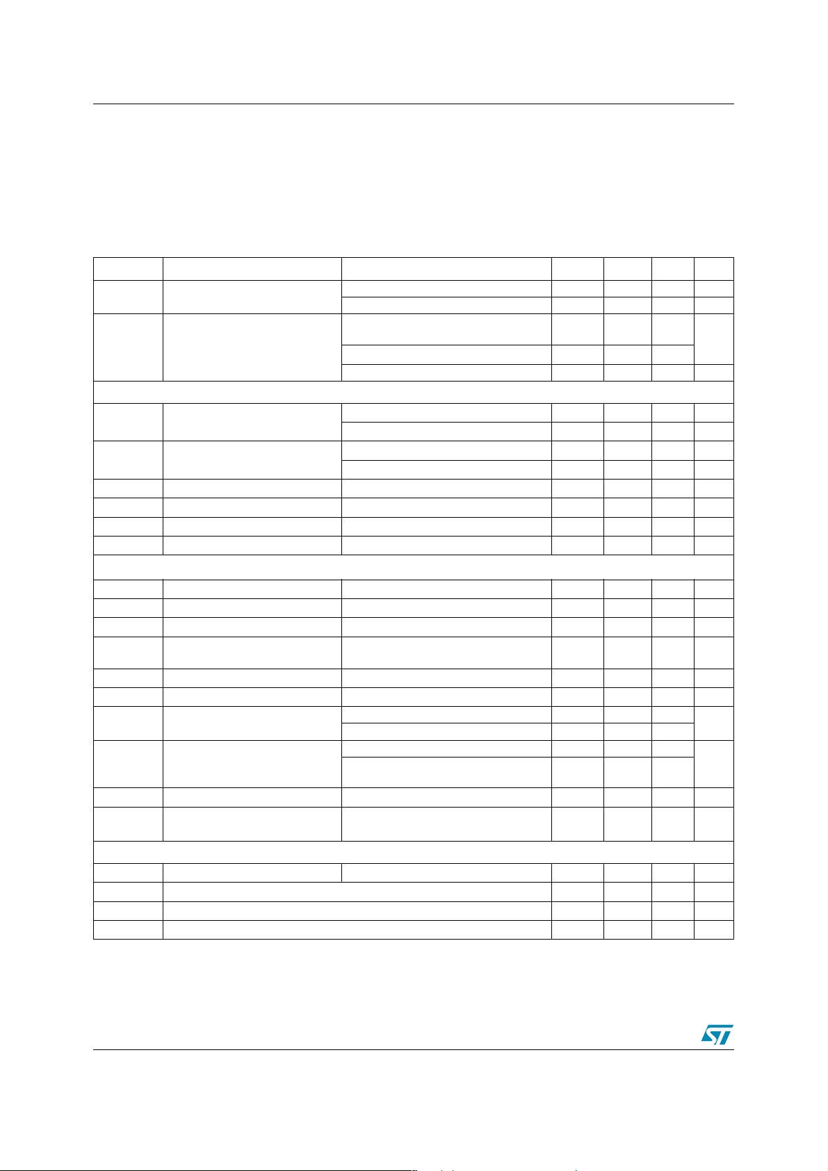
3 Electrical characteristics
Table 6. Electrical characteristics
Characteristics measured over recommended operating conditions unless otherwise is
noted. All typical values are referred to T
C
= 220nF, CT = 4.7µF and C
EXT
Symbol Parameter Test Conditions Min. Typ. Max. Unit
I
BAT
I
Digital Part Supply Current
IF
Operating Supply Current
LOGIC INPUTS AND OUTPUTS
V
V
V
V
I
LKG
I
OZ
V
BUS
V
BUS
V
BUS_LKGVBUS
V
BUS_RIPVBUS
f
CP
R
VBUSVBUS
I
VBUS
V
BUS_VLD
HIGH level output voltage
OH
LOW level output voltage
OL
HIGH level input voltage
IH
LOW level input voltage
IL
Input leakage current -1 1 µA
Off-state output current -5 5 µA
V
output voltage I
BUS
leakage voltage
output ripple I
Charge-pump switching
frequency (2)
input impedance
Maximum V
V
valid comparator
BUS
source current C
BUS
threshold
Session valid comparator
V
SES_VLD
threshold for both A and B
devices
R
VBUS_PUVBUS
R
VBUS_PD
charge pull-up resistance
V
discharge pull-down
BUS
resistance
ID
V
ID_BIAS
R
ID_PU
R
ID_GND
R
ID_FLOAT
ID pin bias voltage
ID pin pull-up resistance 70 105 130 kΩ
ID line short resistance to detect id_gnd state 10 Ω
ID line short resistance to detect id_float state 800 kΩ
TRM
Active mode (1,2) 0.6 1.6 mA
Power down mode 1 µA
Transceiver current while
transmitting and receiving (1,2)
Charge pump current, I
Power down mode (3) 1 µA
= -100µA VIF-0.15
I
OH
I
= -2mA VIF-0.40
OH
= 100µA
I
OL
I
= 2mA
OL
= 8mA
LOAD
No Load 3 200 mV
= 8mA, CT = 4.7µF
LOAD
= 220 nF, V
EXT
Low to high transition 4.40
High to low transition 4.40
Low to high transition 0.8 2.0
High to low transition 0.8 2.0
= 140kΩ, V
R
CP_ID
= 25°C, VIF = 1.8V, V
A
= 1µF
LOAD
> 4.4V
BUS
≤ 5V
BAT
= 8mA
= 3.3V, RS = 20Ω,
BAT
4.5 7
17 25
0.15 V
0.40 V
0.7V
IF
0.3V
IF
4.4 4.9 5.25 V
30 60 mV
0.5 0.8 1.5 MHz
40 76 100 kΩ
20 35 mA
281 640 Ω
656 1260 Ω
1.3 1.9 3.0 V
mA
V
V
V
V
V
V
6/26
Page 7
STOTG04ES Electrical characteristics
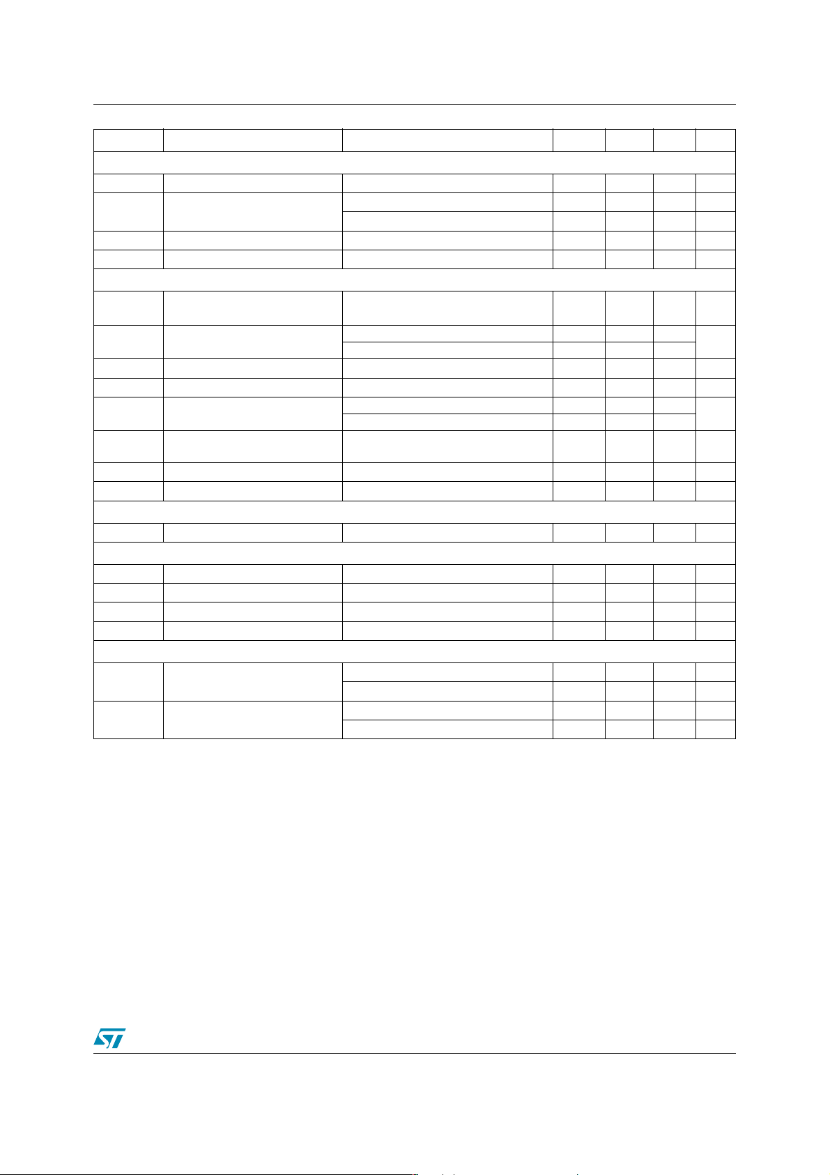
Symbol Parameter Test Conditions Min. Typ. Max. Unit
DIFFERENTIAL DRIVER
Z
DRV
V
OH_DRV
V
OL_DRV
V
CRS
Output Impedance
HIGH level output voltage
LOW level output voltage
Driver crossover voltage
DIFFERENTIAL AND SINGLE-ENDED RECEIVERS
V
V
SE-TH
R
C
R
PU_D+
R
PU_D-
R
V
DT_LKG
Differential receiver input
DI
sensitivity (V
D+
- VD-)
SE receivers switching
threshold
Input resistance PU/PD resistor deactivated 1.5 MΩ
IN
Input capacitance 10 30 pF
IN
Data line pull-up resistance on
pin D+
Data line pull-up resistance on
pin D-
Data line pull-down resistance 14.25 17.0 24.8 kΩ
PD
Data line leakage voltage
CAR KIT INTERRUPT DETECTOR
V
CR_INT_TH
Car kit Interrupt threshold 0.4 0.6 V
UART MODE – D+ AND D- PINS
V
V
V
V
HIGH level output voltage
OH
LOW level output voltage
OL
HIGH level input voltage 2.0 V
IH
LOW level input voltage 0.8 V
IL
VOLTAGE REGULATOR
V
TRM
I
TRM
(1) Transmitting and receiving at 12Mbit/s, loads of 50pF on D+ and D- pins, no capacitive loads on VP and VM pins
(2) Not tested in production; characterization only
(3) See paragraph 6.7.1
Internal power supply voltage
Voltage regulator output
current
Excluding external R
= 14.25kΩ, V
R
LH
RLH = 14.25kΩ, V
= 1.425kΩ
R
LL
= 50 to 600pF
C
LOAD
= 0.8 to 2.5V
V
CM
TRM
TRM
S
= 3.3V
= 2.7V
81624Ω
2.8 3.6 V
2.6 3.0 V
00.3V
1.3 1.67 2.0 V
-200 200 mV
Low to high transition 0.8 1.6 2.0
High to low transition 0.8 1.1 2.0
Bus Idle 900 1300 1575
Receiving mode 1425 2200 3090
900 1300 1575 Ω
R
I
I
V
V
V
V
OH
OL
= 300kΩ
PU_EXT
= -2mA
= 2mA
= 3.3 to 5V, no load; uart_en=0
BAT
= 2.8 to 5V, no load; uart_en=1
BAT
= 3.6V, V
BAT
= 3.0V, V
BAT
> 3V; uart_en=0
TRM
>2.6V; uart_en=1
TRM
200 342 mV
2.4 3.6 V
00.4V
3.0 3.3 3.6 V
2.6 2.75 2.9 V
20 mA
10 mA
V
Ω
7/26
Page 8
Electrical characteristics STOTG04ES
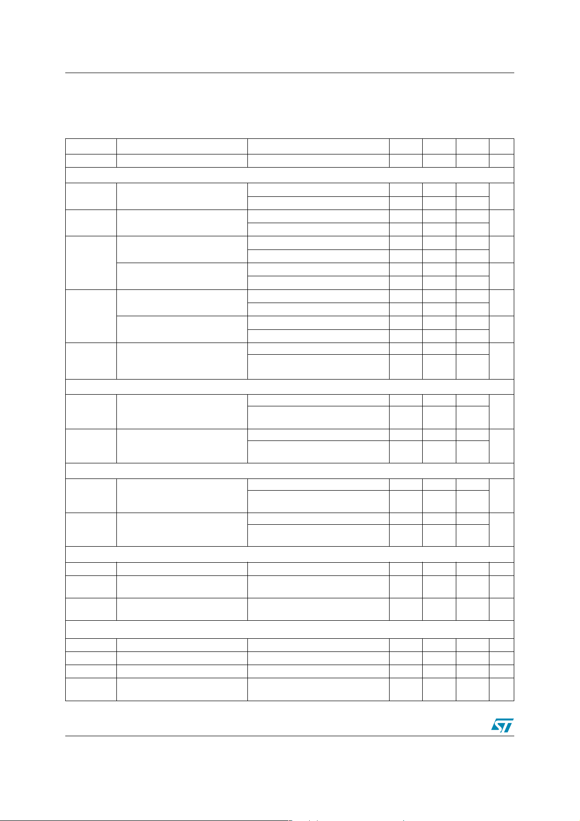
Table 7. Switching characteristics
Over recommended operating conditions unless otherwise is noted. All the typical values are
referred to T
= 1µF
C
TRM
Symbol Parameter Test Conditions Min. Typ. Max. Unit
T
VBUS_RISEVBUS
DIFFERENTIAL DRIVER
t
R
t
F
t
P_DRV_R
t
P_DRV_F
t
RFM
SINGLE-ENDED RECEIVERS
t
P_SE_R
t
P_SE_F
DIFFERENTIAL RECEIVER
t
P_DIF_R
t
P_DIF_F
DIGITAL INTERFACE
t
SET_OE
t
TA _ OI
t
TA _ IO
I2C BUS (3)
f
SCL
t
LOW
t
HIGH
t
IICR
rise time I
Data signal rise time
Data signal rise time
Propagation delay of the driver,
rising edge; DAT_SE0 mode
Propagation delay of the driver,
rising edge; VP_VM mode
Propagation delay of the driver,
falling edge; DAT_SE0 mode
Propagation delay of the driver,
rising edge; VP_VM mode
Rise and fall time matching (tR/
tF) excluding the first transition
from the idle state
Propagation delay of the SE
receiver, rising edge
Propagation delay of the SE
receiver, falling edge
Propagation delay of the SE
receiver, rising edge
Propagation delay of the SE
receiver, falling edge
Output enable setup time 50 ns
Output to input bus turnaround
time (1, 2)
Output to input bus turnaround
time (1, 2)
SCL clock frequency 100 kHz
Low period of the SCL clock 4.7 µs
High period of the SCL clock 4.0 µs
Rise time of both SDA and SCL
signals
= 25°C, VIF = 1.8V, V
A
LOAD
Full-speed mode, C
Low-speed mode, C
Full-speed mode, C
Low-speed mode, C
Full-speed mode, C
Low-speed mode, C
Full-speed mode, C
Low-speed mode, C
Full-speed mode, C
Low-speed mode, C
Full-speed mode, C
Low-speed mode, C
Full-speed mode 90 111.11
Low-speed mode 80 125
Full-speed mode, input slope 15ns 18
Low-speed mode, input slope
150ns
Full-speed mode, input slope 15ns 18
Low-speed mode, input slope
150ns
Full-speed mode, input slope 15ns 24
Low-speed mode, input slope
150ns
Full-speed mode, input slope 15ns 24
Low-speed mode, input slope
150ns
= 3.3V, RS = 20Ω, C
BAT
= 8mA, CT = 10µF
LOAD
LOAD
LOAD
LOAD
LOAD
LOAD
LOAD
LOAD
LOAD
LOAD
LOAD
LOAD
= 50pF
= 600pF
= 50pF
= 600pF
= 50pF
= 600pF
= 50pF
= 600pF
= 50pF
= 600pF
= 50pF
= 600pF
= 220nF, CT = 4.7µF, and
EXT
1100ms
48.520
75 110 300
48.520
75 110 300
38
280
55
300
38
280
55
300
ns
ns
ns
ns
ns
ns
%
18
18
24
24
ns
ns
ns
ns
05ns
05ns
1000 ns
8/26
Page 9
STOTG04ES Electrical characteristics
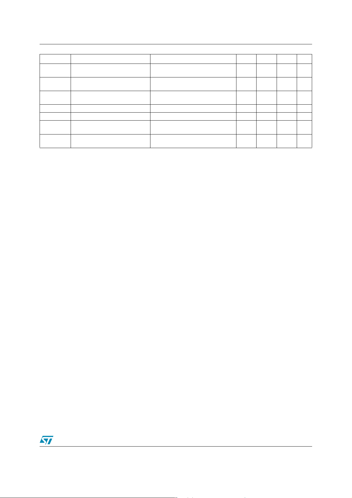
Symbol Parameter Test Conditions Min. Typ. Max. Unit
t
IICF
t
SU_STA
t
HD_STA
t
SU_DAT
t
HD_DAT
t
SU_STO
t
BUF
NOTE 1: Parameter applies to the OE_TP_INT/, DAT_VP, and SE0_VM signals
NOTE 2: Not tested in production; characterization only
NOTE 3: Requirements defined by the I2C-Bus Specification, version 2.1
Fall time of both SDA and SCL
signals
Setup time for a repeated START
condition
Hold time for the START and
repeated START conditions
4.7 µs
4.0 µs
300 ns
Data setup time 250 ns
Data hold time 0 µs
Setup time for the STOP
condition
Bus free time between a STOP
and START condition
4.0 µs
4.7 µs
9/26
Page 10
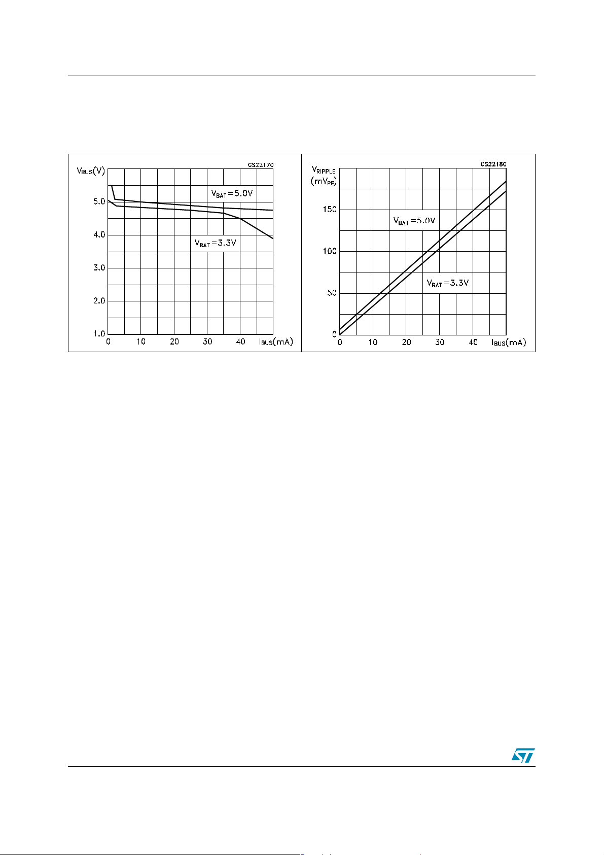
Charge pump characteristics STOTG04ES
4 Charge pump characteristics
Figure 3. Output characteristics Figure 4. Output ripple
10/26
Page 11
STOTG04ES Timing diagrams
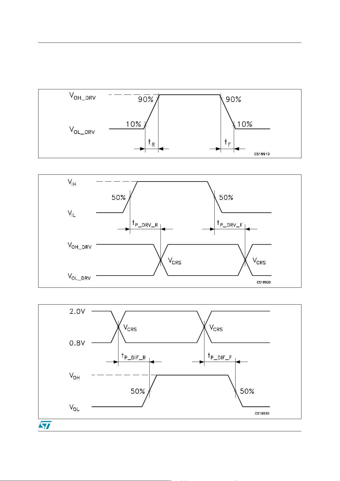
5 Timing diagrams
Figure 5. Rise and fall times
Figure 6. Differential driver propagation delay
Figure 7. Differential receiver propagation delay
11/26
Page 12
Timing diagrams STOTG04ES
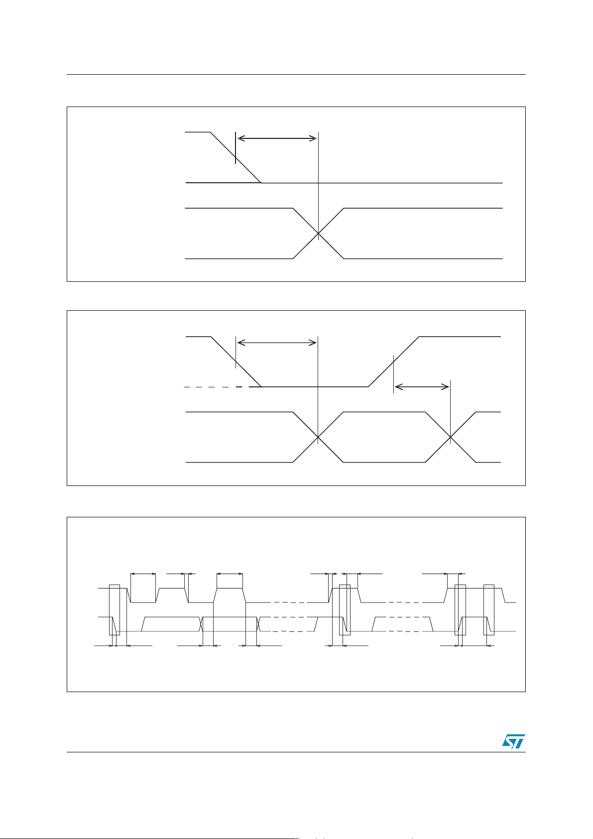
Figure 8. Output enable setup time
t
V
IH
SET_OE
OE_TP_INT/
V
IL
V
IH
DAT_VP
SE0_VM
V
USB Idle State Data to Transmit
IL
Figure 9. Bus turnaround time
t
V
IH
TA_OI
OE_TP_INT/
DAT_VP
SE0_VM
Figure 10. I
SCL
SDA
t
IIC_F
V
IL
V
IH
V
IL
2
C BUS timing
t
t
LOW
IIC_F
t
HD_STA
t
SU_DAT
t
TA_IO
output input output
t
HIGH
t
HD_DAT
t
IIC_R
t
HD_STA
SrS P S
t
SU_STA
t
SU_STO
t
IIC_R
t
BUF
12/26
Page 13
STOTG04ES Timing diagrams
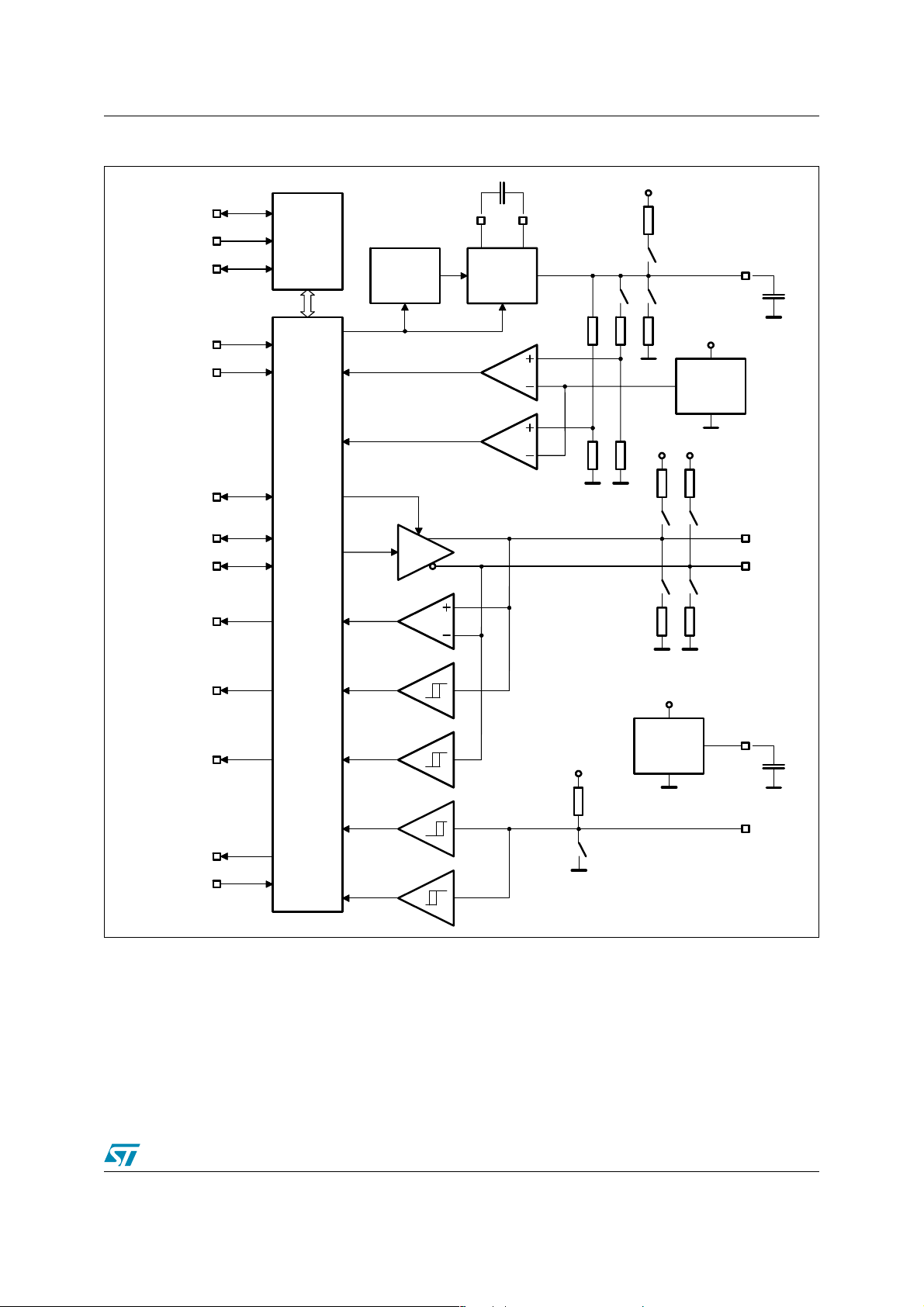
Figure 11. Block diagram
VBAT
ADR_PSW
SCL
SDA
SPEED
SUSPEND
OE_TP_INT/
DAT_VP
SE0_VM
RCV
CAP2CAP1
I2 C
In te rfa c e
O sc illa to r
Charge
Pump
VBUS
VBAT
Bandgap
Reference
VTRM
D+
D-
and
Register Set
Control Logic
VP
VM
IN T /
RESET/
VBAT
VBAT
Voltage
Regulator
VTRM
ID
13/26
Page 14

Block description STOTG04ES
6 Block description
The STOTG04ES integrates a charge pump and comparators for the V
switch, differential data driver, differential and single-ended receivers, low dropout voltage regulator and
control logic. The STOTG04ES provides a complete solution for connection of a digital USB OTG
controller to the physical Universal Serial Bus.
, ID line detector and interrupt
BUS
6.1 Charge pump
The V
load current. The charge pump can be powered by voltage from 2.7V to 5.5V. It needs two capacitors for
its operation: an external capacitor of 220nF connected between the CAP1 and CAP2 pins and a 4.7µF
decoupling tank capacitor on the V
possible to provide it using an external charge pump or switch controlled by the ADR_PSW pin.
6.2 V
These comparators monitor the V
V
BUS
voltage is above V
line voltage is provided using the internal charge pump. It is capable of sourcing up to 35mA
BUS
. In case when an application needs higher current than 35mA, it is
BUS
Comparators
BUS
voltage. They provide current status information for the V
valid status means that the voltage is above V
SES_VLD
level.
BUS
BUS_VLD
. Session valid status means that the V
BUS
line.
BUS
6.3 Voltage regulator
An internal low-dropout voltage regulator provides power supply for the bus drivers and receivers. The
regulator needs an external capacitor of 1µF on the V
provide 3.3V or 2.75V output voltages according to the Operating Mode.
The regulator can be bypassed in case when the analog supply voltage is in the range of 3.0V (or 2.7V)
to 3.6V. It is necessary to tie the V
pin to the V
TRM
BAT
pin for its proper operation. The regulator can
TRM
power supply voltage to bypass the regulator.
6.4 ID Line detector
This block senses ID line status. It is capable of detecting three different line states:
• pin floating;
• pin tied to ground;
• pin grounded via a 140kΩ resistor.
The ID detector can also generate an interrupt by shorting the pin to ground.
6.5 Driver and receivers
The driver can operate in two different modes. It can act as a simple low-speed and full-speed differential
USB driver or as two independent single-ended drivers in the UART mode.
This block contains one differential receiver for the USB operation mode and two single-ended receivers
for USB signaling as well as UART receivers.
14/26
Page 15
STOTG04ES Block description
6.6 Control logic
This block controls the behavior of whole chip. It communicates with the external environment via the I2C
serial bus. The control logic block consists of I
2
C slave interface, configuration and status registers, and
some glue logic.
6.7 Modes of operation
The STOTG04ES can operate in two different power modes and in three operating modes. They can be
controlled by logic signals and control registers.
6.7.1 Power modes
To reduce power consumption when there is no need for the USB function, the STOTG04 implements
power-down mode. In this mode, the power consumption is strongly reduced. Power mode of the device
can be controlled by bit suspend of the Control Register 1 or/and the SUSPEND pin as can be seen in
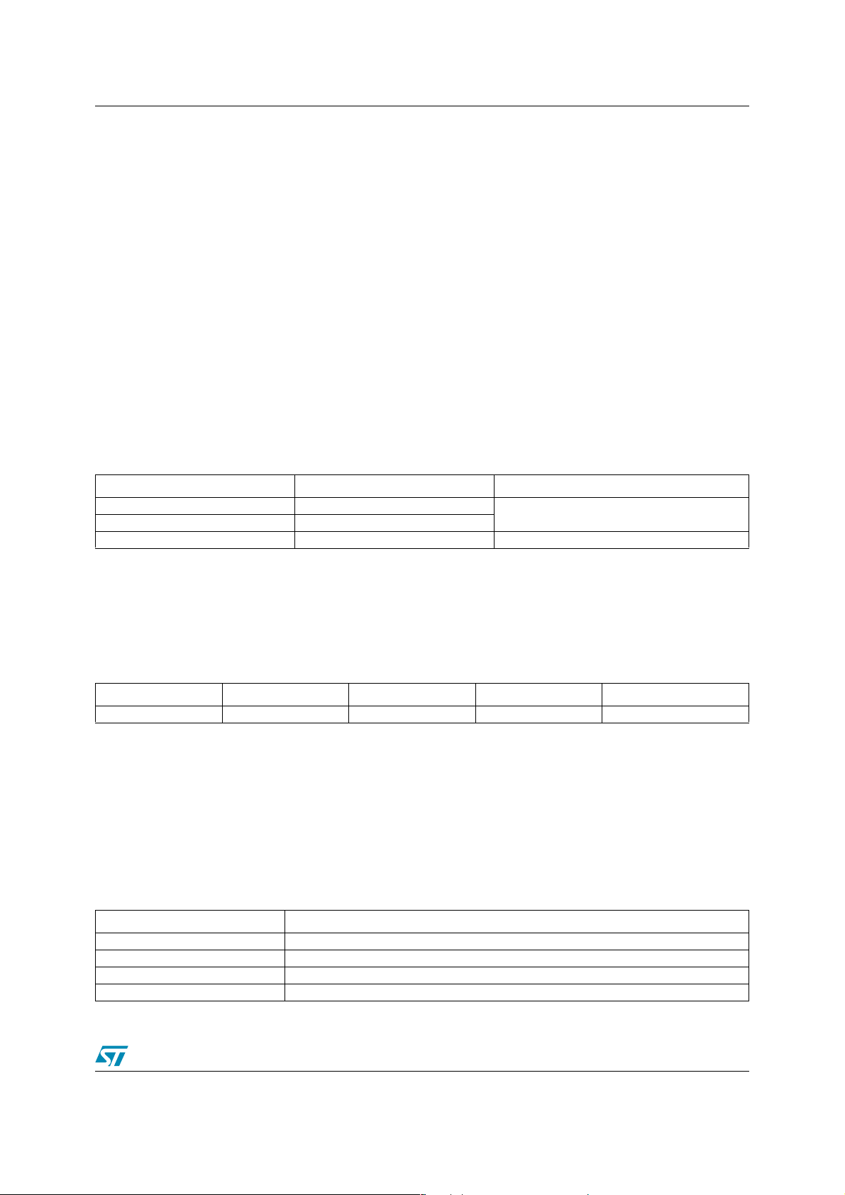
table 8).
Table 8. Power modes
SUSPEND BIT SUSPEND PIN Power Mode
0X
X0
1 1 power-down
Although in power down mode all analog blocks should be switched off, some of them could be turned on
by bits in the control registers having higher priority than suspend bit. In order to obtain minimum power
consumption in power down mode the device must be configured has shown in Table 9. The digital part is
fully static so that it almost does not consume power. All of the interrupts (except BDIS_ACON) are fully
operational in Power-down mode, as is the I
2
C interface.
normal operation
Table 9. Power down mode setup
SUSPEND BIT SUSPEND PIN Control register 1 Control register 2 Control register 3
1 1 X1X0XX0- 00XX00X0 -XXXX0XX
X = Don’t care
- = Reserved
Bit order: 0...7
6.7.2 USB Modes
The STOTG04ES transceiver has two basic USB operational modes. These modes define how the digital
IO pins of the transceiver will be used. Independently of USB operating mode, some signals always have
the same function (see Table 10).
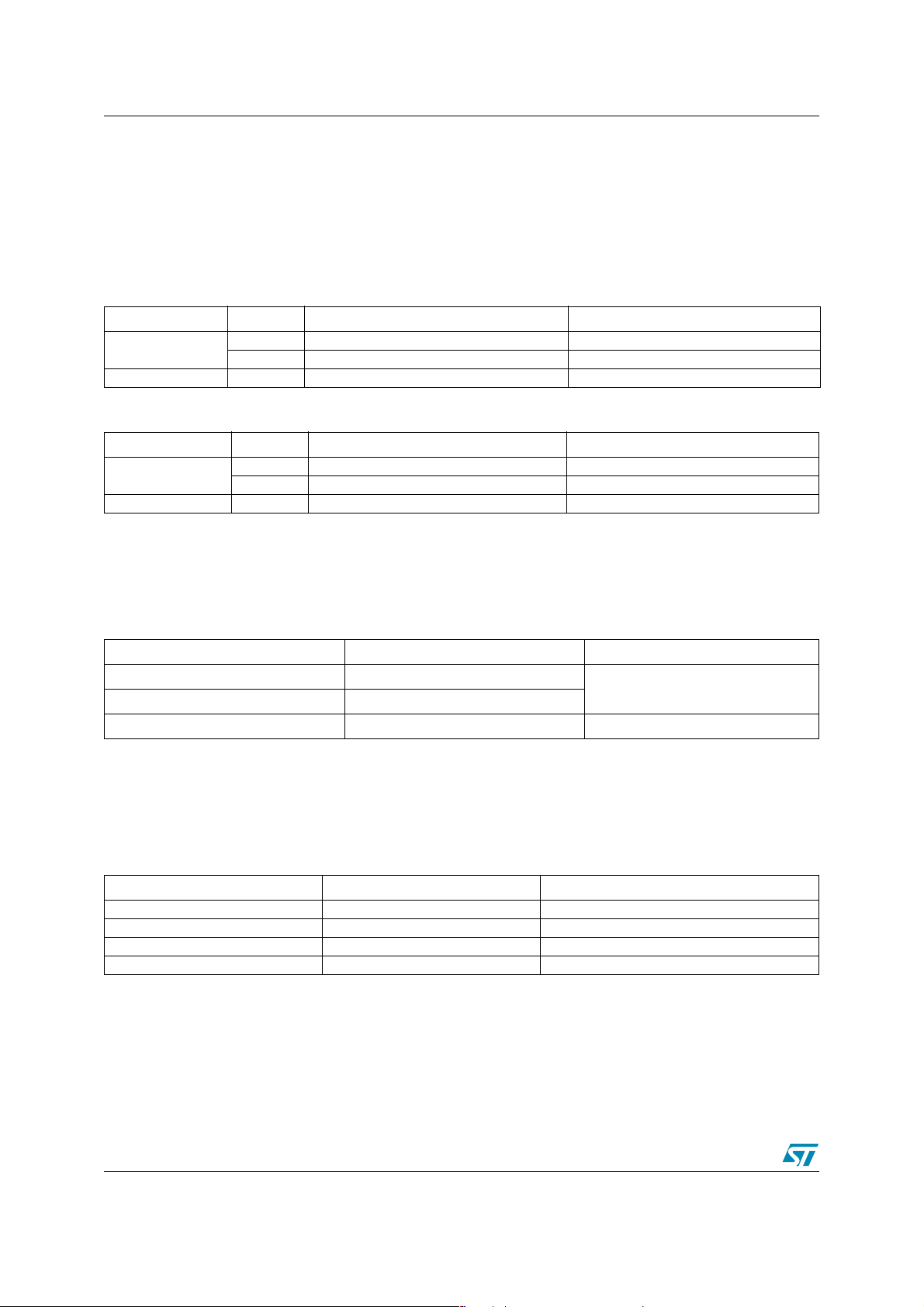
Table 10. Digital interface signals
Signal Function
RCV Differential receiver output
VP D+ single-ended receiver output
VM D- single-ended receiver output
OE_TP_INT/ Output enable signal of the differential driver
15/26
Page 16
Block description STOTG04ES
The RCV signal is active in the VP_VM mode only. Its output driver is controlled by the OE_TP_INT/
signal. Operating modes are described below. The meanings of the DAT_VP and SE0_VM signals
depend on the mode of operation. Both of these signals can be bidirectional or unidirectional. The
direction is controlled by bidi_en Bit of Control Register 3 (described later). When these signals are
bidirectional, the direction is controlled by the OE_TP_INT/ signal (see Tables 11 and 12).
The actual mode of operation is controlled by the dat_se0 Bit of Control Register 1 (see Tables 11 and 12)
Table 11. DAT_SE0 (dat_se0 = 1)
bidi_en OE/* DAT_VP SE0_VM
1
0 X Differential driver input SE0 driver input
0 Differential driver input SE0 driver input
1 Differential receiver output SE0 detector output
Table 12. VP_VM (dat_se0 = 0)
bidi_en OE/* DAT_VP SE0_VM
1
0 X D+ driver input D- driver input
* State of the OE_TP_INT/ signal.
0 D+ driver input D- driver input
1 D+ receiver output D- receiver output
In the USB mode of operation it is necessary to control the rise and fall times of the transmission driver.
These times are different for low-speed and full-speed USB settings. Selection of actual USB speed can
be done using the bit speed of Control Register 1 or/and the SPEED pin (see table 13).
Table 13. USB Speed Selection
speed bit SPEED Pin USB Mode
0X
X0
1 1 full-speed
low-speed
6.7.3 UART Mode
The actual mode of operation is selectable by the transp_en and uart_en Bits of Control Register 1 (see
table 14).
Table 14. Transceiver modes
transp_en uart_en STOTG04 Mode
00 USB
01 UART
1 0 FORBIDDEN
11 UART (1)
(1) In reality, it is not possible to set both these bits at the same time. In this case, only uart_en bit will remain set.
In the UART mode it is possible to select driver direction on both the D+ and D– pins. The selection is
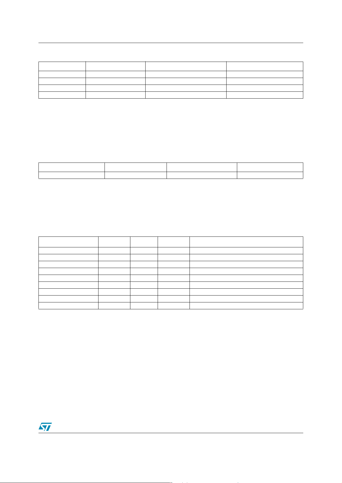
done using the bdir[1] and bdir[0] Bits of Control Register 3 (see table 15).
16/26
Page 17
STOTG04ES Block description
Table 15. UART drivers direction
bdir[1] bdir[0] DAT_VP ↔ D+ SE0_VM ↔ D-
00 →→
01 →←
10 ←→
11 ←←
6.7.4 Audio mode
In this mode the transceiver has to release all of its drivers and pull-up/pull-down resistors on the D+, Dand ID pins, leaving them in a high impedance state. This allows these lines to be used for transmission
of audio signals. The transceiver should not provide voltage on its V
output in this mode. Conditions
BUS
described in Table 16 force the transceiver into the audio mode.
Table 16. Audio mode setup
transp_en bit uart_en bit OE_TP_INT/ signal Control Register 2
0 0 1 00000000
6.8 Registers
The STOTG04ES transceiver device is controlled using register settings (see Table 17). These registers
can be set and read via the I
2
C bus.
Table 17. Register set
Register Size (bits)
Vendor ID 16 r 00h STMicroelectronics ID (0483h) - LSB first
Product ID 16 r 02h ID of the STOTG04 (A0C4h) - LSB first
Control 1 8 r/s/c 04h 05h First Control Register
Control 2 8 r/s/c 06h 07h Second Control Register
Control 3 8 r/s/c 12h 13h Third Control Register
Interrupt Source 8 r 08h Current state of signals generating interrupts
Interrupt Latch 8 r/s/c 0Ah 0Bh Latched source that generated interrupt
Interrupt Mask False 8 r/s/c 0Ch 0Dh Enables interrupts on falling edge
Interrupt Mask True 8 r/s/c 0Eh 0Fh Enables interrupts on rising edge
(1) Access type can be: read (r), set (s), clear (c).
(2) The first address is to set, the second one to clear bits.
Acc
(1)
Addr
(2)
Description
When writing to the set address, any “1” will set the associated Bit to logic “1”. When writing to the clear
address, any “1” will set the associated Bit to logic “0”. It is possible to read from any address, whether it
is a set or clear address. See Tables 18, 19, 20, 21 for bit setting details.
17/26
Page 18
Block description STOTG04ES
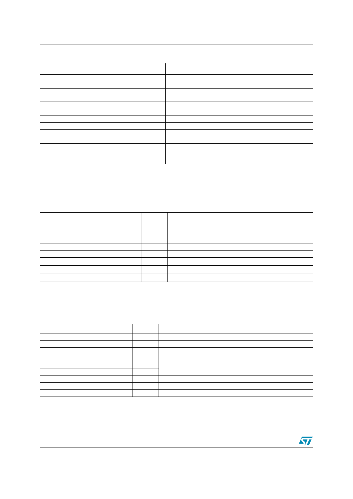
Table 18. Control register 1
Name Bit
Speed 0 1
Suspend 1 1
dat_se0 2 0
transp_en 3 0 Reserved. For testing purpose
bdis_acon_en 4 0 Enable A-device to connect if B-device disconnect detected
oe_int_en 5 0
uart_en 6 0
7 Reserved
(1) State of the bit after reset.
(1)
R
0 = low-speed mode
1 = full-speed mode
0 = normal operation
1 = power-down mode
0 = VP_VM mode
1 = DAT_SE0 mode
When set and suspend = 1, then OE_TP_INT/ becomes
interrupt output
Enables UART mode (higher priority than transp_en bit) and
2.7V voltage regulation
Description
Setting the bdis_acon_en bit enables automatic switching of the D+ pull-up resistor when the device
receives an SE0 longer than half of the bit period. This function should not be used in low-speed
operation.
Table 19. Control register 2
Name Bit R Description
dp_pull-up 0 0 Connect D+ pull-up
dm_pull-up 1 0 Connect D- pull-up
dp_pull-down 2 1 Connect D+ pull-down
dm_pull-down 3 1 Connect D- pull-down
id_gnd_drv 4 0 Connect ID pin to ground
vbus_drv 5 0
vbus_dischrg 6 0
vbus_chrg 7 0
Provide power to V
Discharge V
Charge V
through a resistor to ground
BUS
through a resistor
BUS
BUS
It is not possible to set vbus_drv, vbus_dischrg and vbus_chrg at the same time; the bit having higher
priority will remain set while the others will be cleared. Vbus_drv has higher priority than vbus_dischrg
which has higher priority than vbus_chrg.
Table 20. Control register 3
Name Bit R Description
00Reserved
rec_bias_en 1 0 Enables transmitter bias even during USB receive
bidi_en 2 1
bdir[0] 3 0
bdir[1] 4 1
audio_en 5 0 Enables car-kit interrupt detector
psw_en 6 0 Enables external charge pump control on the ADR_PSW pin
70Reserved
18/26
When set, then DAT_VP and SE0_VM pins become bidirectional
otherwise they are inputs only
Direction of the drivers between DAT_VP↔DP and
SE0_VM↔DM in the UART mode
Page 19
STOTG04ES Block description
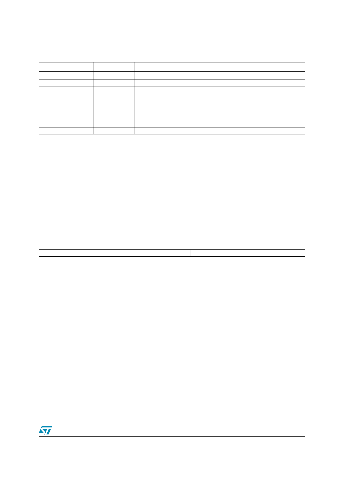
Table 21. Interrupt registers (*)
Name Bit R Description
vbus_vld 0 0
sess_vld 1 0 Session valid comparator
dp_hi 2 0 D+ pin is asserted high during SRP
id_gnd 3 0 ID pin grounded
dm_hi 4 0 D- pin is asserted high
id_float 5 0 ID pin floating
bdis_acon 6 0
cr_int 7 0 Car-kit interrupt
(*) Bit order is the same for all four interrupt related registers. Meaning of each register is described in Table 17.
A-device V
Set when bdis_acon_en bit is set and transceiver asserts dp_pull-up after
detecting B-device disconnect
valid comparator
BUS
6.9 I2C Bus interface
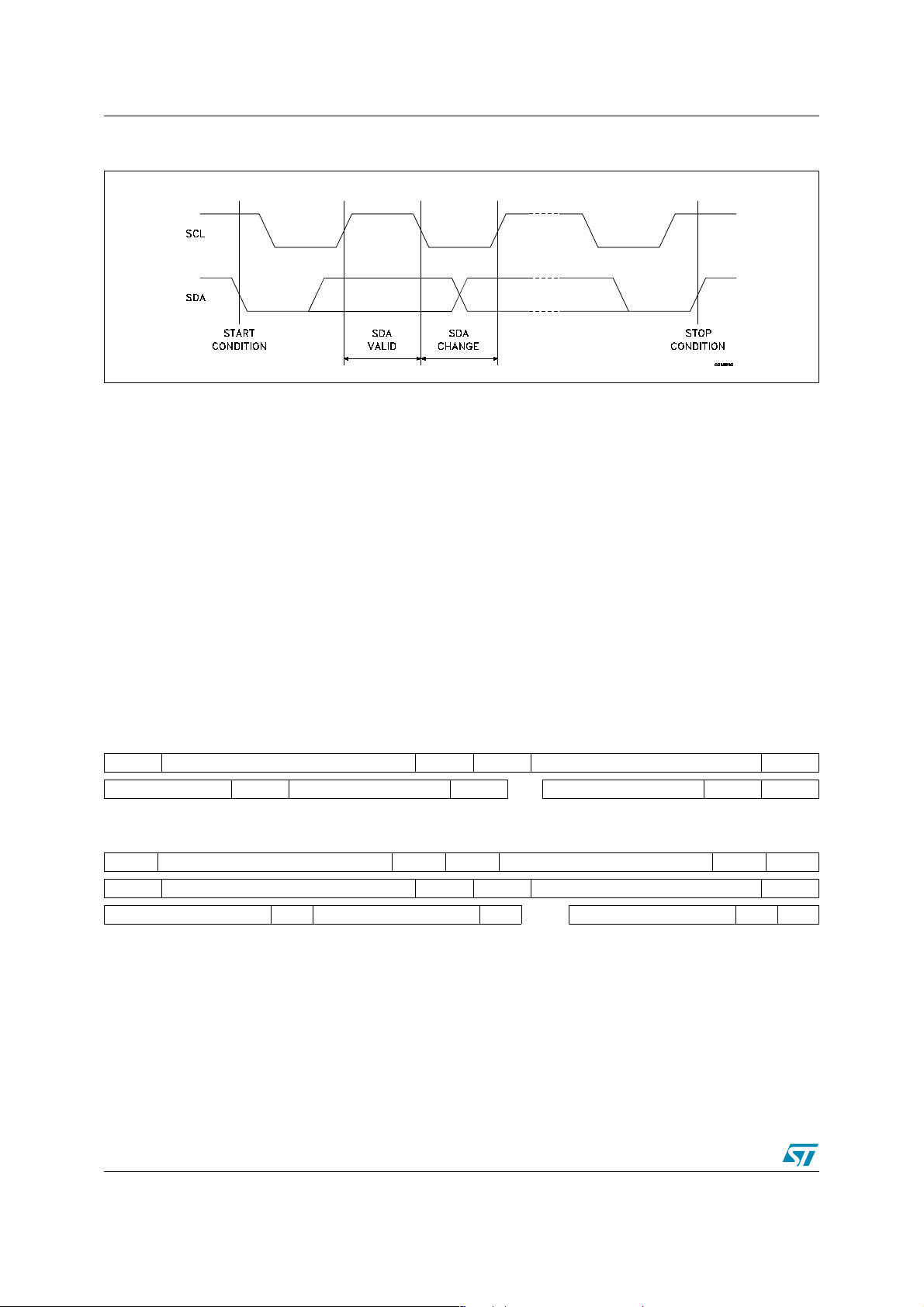
All of the STOTG04 transceiver registers are accessible through the I2C bus (see Figure 12). The device
contains a slave controller which provides communication with an external master. The I
2
C interface
consists of three pins:
• SDA (Serial Data);
• SCL (Serial Clock);
• ADR_PSW (is the LSB of the device address).
6.10 Device address
The USB-OTG transceiver has following 7-bit I2C device address:
010110adr
The adr bit represents current state of the ADR_PSW device pin. It means that the address can be either
2Ch or 2Dh according to the ADR_PSW pin.
6.11 Bus protocol
Any device that sends data to the bus is defined as the transmitter. Any device that reads the data is the
receiver. The device that controls data transfers is the bus master, while the transmitter or receiver is the
slave device. The master initiates data transfers and provides the serial clock. The STOTG04 is always
the slave device.
Operation of the I
2
C bus is described by following figure 12.
19/26
Page 20
Block description STOTG04ES
Figure 12. Basic operation of the I2C Bus
Start condition is identified by a falling edge of the SDA signal while the SCL is stable at high level. The
start condition must precede any data transfer on the bus.
Stop condition is identified by a rising edge of the SDA signal while the SCL is stable at high level. The
stop condition terminates any communication between device and master.
The acknowledge bit is used to indicate a successful byte transfer. The bus transmitter releases the SDA
line after sending eight data bits. During the ninth clock period the receiver pulls the SDA line low to
acknowledge the receipt of the eight data bits. If the receiver is a slave device and it does not generate
acknowledge bit then the bus master can generate the stop condition in order to abort the transfer.
Below is described format of I
2
C commands. All tables use common format and symbols. Every data
word consists of eight bits with most significant bit first and least significant bit last.
Symbols used in the tables are:
• S – start condition
• P – stop condition
• A – acknowledge bit
• N – negative acknowledge
WRITE Command to the transceiver device is described by following table. It is possible to write into
several consecutive registers during one write command.
S Device address 0 A Reg. address K A
Data (K) A Data (K+1) A .. Data (K+N) A P
READ command consists of dummy write to set proper address of a register followed by real read
sequence.
S Device address 0 A Reg. address K A P
S Device address 1 A Data (K) A
Data (K+1) A Data (K+2) A ... Data (K+N) N P
20/26
Page 21
STOTG04ES Block description
6.12 External charge pump switch
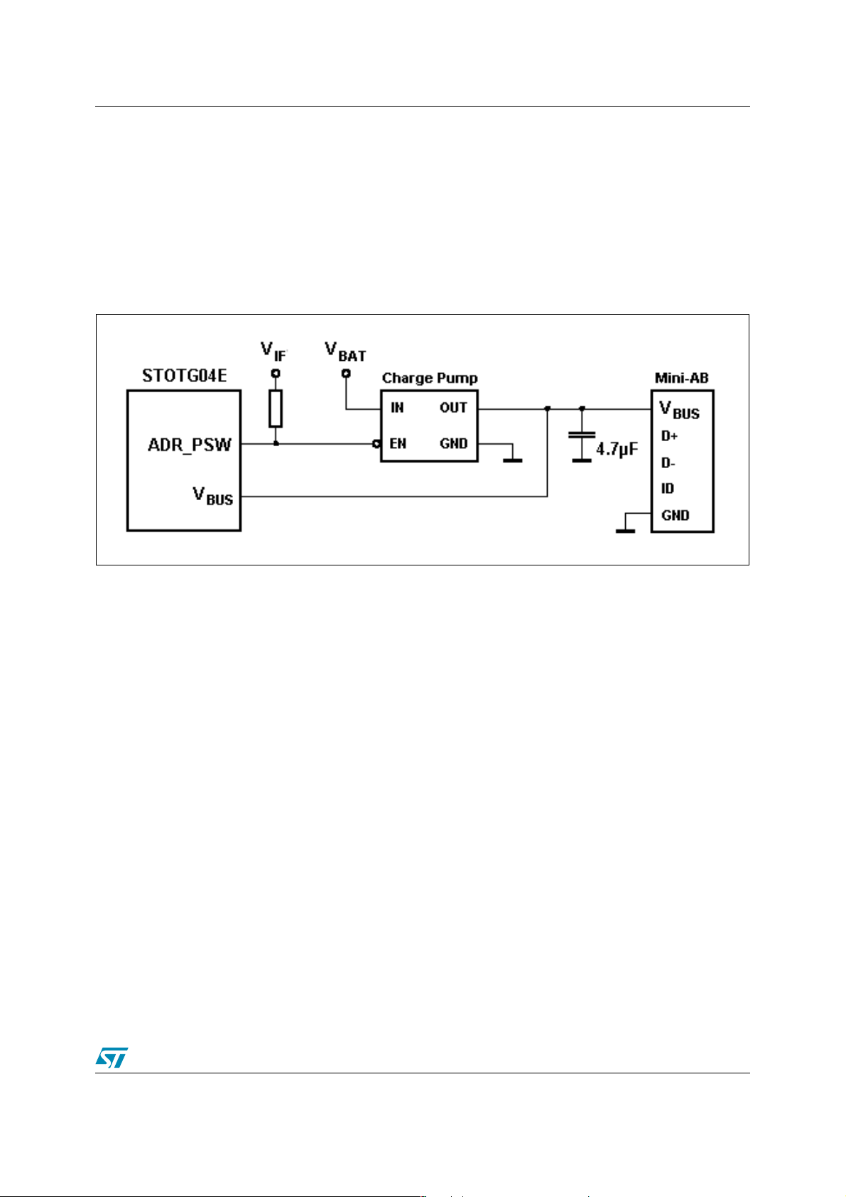
The ADR_PSW pin has two functions. State of this pin is always latched into a register on the rising edge
of the RESET/ signal. The latched value is used as a least significant bit of the I
address is latched, this pin can be set as an output by setting the PSW_EN bit of the Control Register 3.
Output value of the pin is low when the pin is high during reset; otherwise the output is high.
Example connection of an external charge pump is shown in following figure. When the charge pump
control signal would be active high, the ADR_PSW pin should be pulled down instead of high.
Figure 13. External charge pump application
2
C address. After the
21/26
Page 22

Package mechanical data STOTG04ES
7 Package mechanical data
In order to meet environmental requirements, ST offers these devices in ECOPACK® packages.
These packages have a Lead-free second level interconnect. The category of second Level
Interconnect is marked on the package and on the inner box label, in compliance with JEDEC
Standard JESD97. The maximum ratings related to soldering conditions are also marked on
the inner box label. ECOPACK is an ST trademark. ECOPACK specifications are available at:
www.st.com.
22/26
Page 23
STOTG04ES Package mechanical data
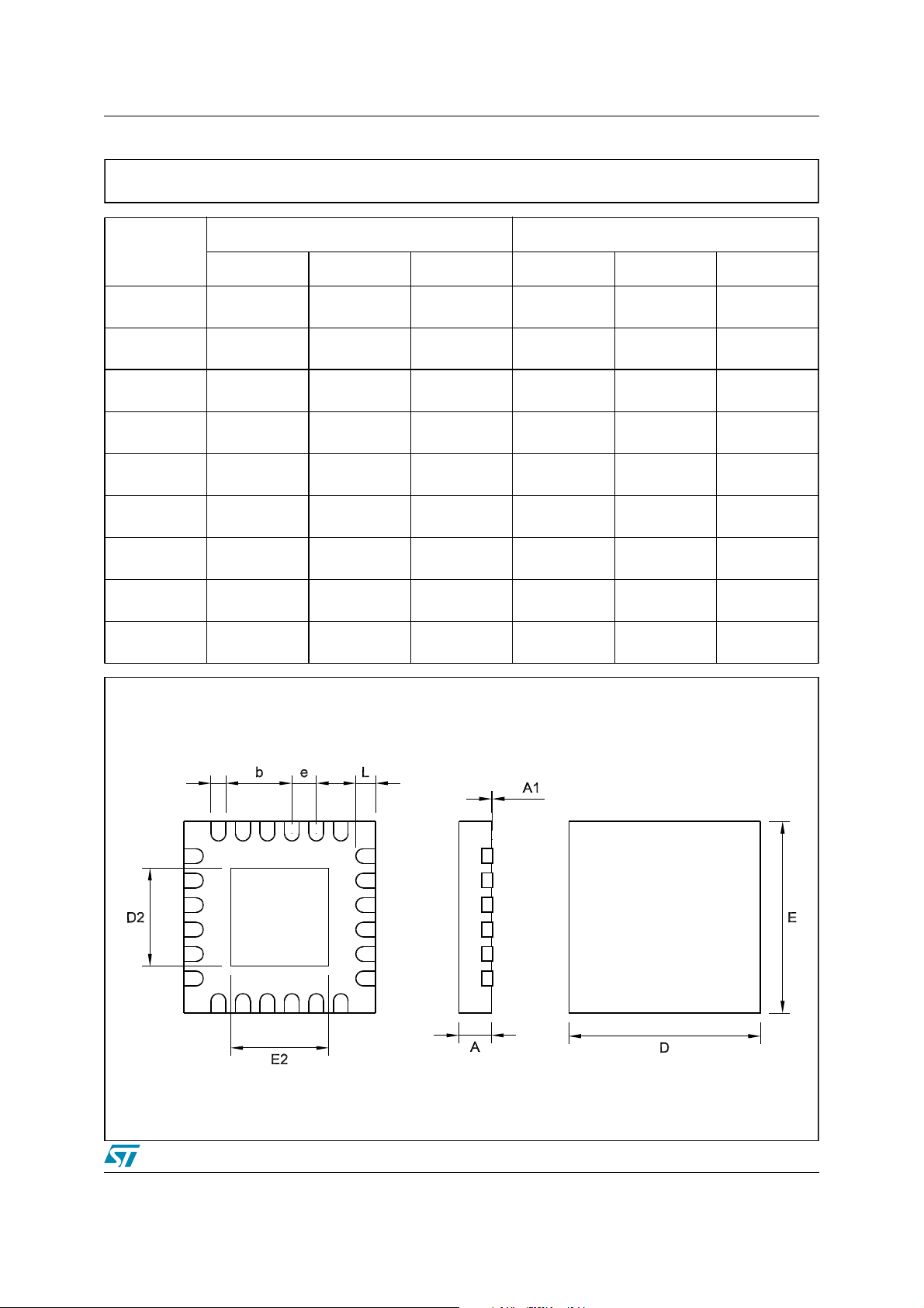
QFN24 (4x4) MECHANICAL DATA
mm. mils
DIM.
MIN. TYP MAX. MIN. TYP. MAX.
A1.0039.4
A1 0.00 0.05 0.0 2.0
b 0.18 0.30 7.1 11.8
D 3.9 4.1 153.5 161.4
D2 1.95 2.25 76.8 88.6
E 3.9 4.1 153.5 161.4
E2 1.95 2.25 76.8 88.6
e0.50 19.7
L 0.40 0.60 15.7 23.6
23/26
Page 24
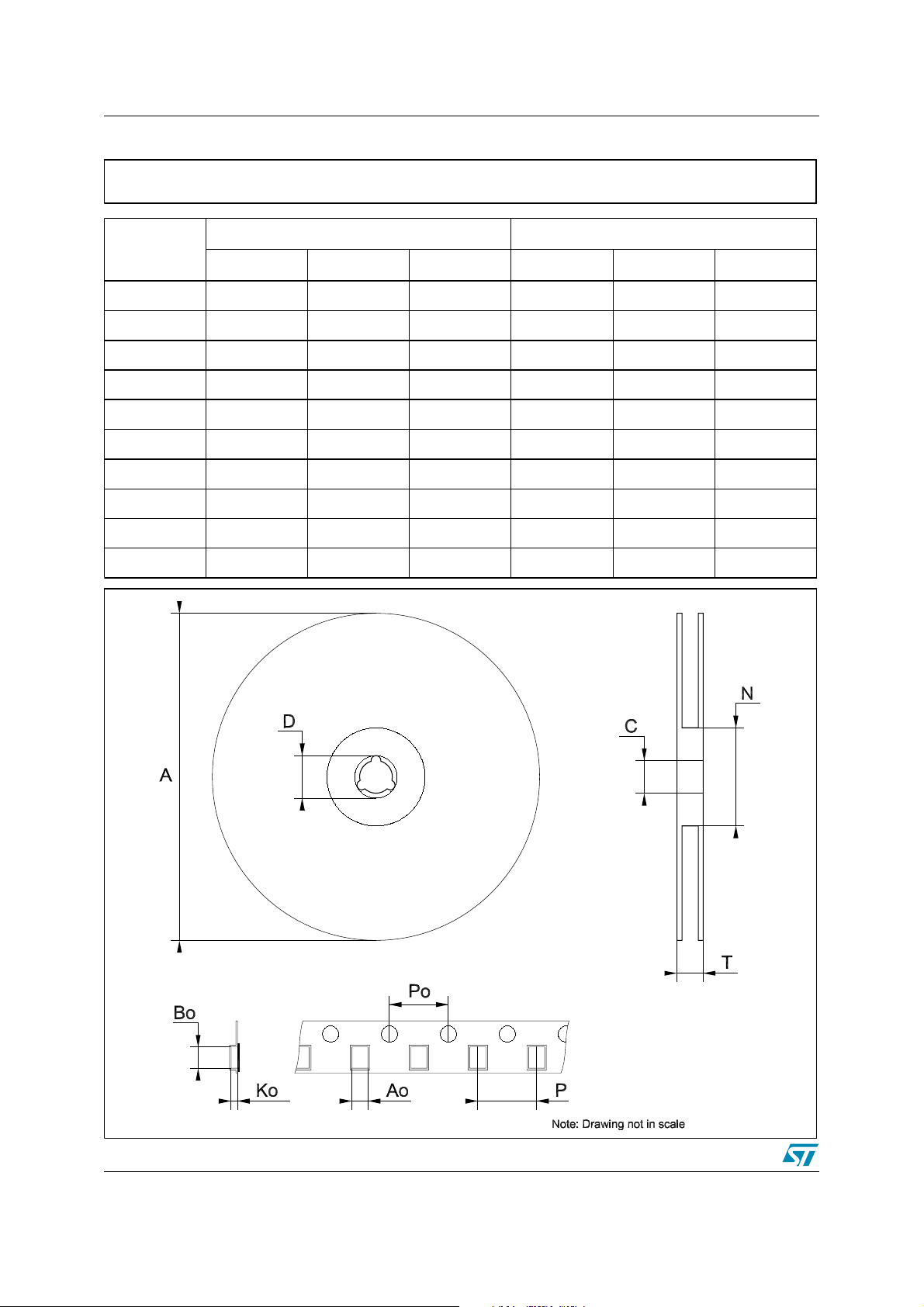
Package mechanical data STOTG04ES
Tape & Reel QFNxx/DFNxx (4x4) MECHANICAL DATA
mm. inch
DIM.
MIN. TYP MAX. MIN. TYP. MAX.
A 330 12.992
C 12.8 13.2 0.504 0.519
D 20.2 0.795
N 99 101 3.898 3.976
T 14.4 0.567
Ao 4.35 0.171
Bo 4.35 0.171
Ko 1.1 0.043
Po 4 0.157
P 8 0.315
24/26
Page 25

STOTG04ES Revision history
8 Revision history
Table 22. Revision history
Date Revision Description of Change
13-Jan-2006 1 First Release.
01-Feb-2006 2 Mistake on Table 1.
17-Oct-2006 3
Added details in paragraph 6.7.1, comments to table 19 and description in
paragraph 6.12.
25/26
Page 26

STOTG04ES
Please Read Carefully:
Information in this document is provided solely in connection with ST products. STMicroelectronics NV and its subsidiaries (“ST”) reserve the
right to make changes, corrections, modifications or improvements, to this document, and the products and services described herein at any
time, without notice.
All ST products are sold pursuant to ST’s terms and conditions of sale.
Purchasers are solely responsible for the choice, selection and use of the ST products and services described herein, and ST assumes no
liability whatsoever relating to the choice, selection or use of the ST products and services described herein.
No license, express or implied, by estoppel or otherwise, to any intellectual property rights is granted under this document. If any part of this
document refers to any third party products or services it shall not be deemed a license grant by ST for the use of such third party products
or services, or any intellectual property contained therein or considered as a warranty covering the use in any manner whatsoever of such
third party products or services or any intellectual property contained therein.
UNLESS OTHERWISE SET FORTH IN ST’S TERMS AND CONDITIONS OF SALE ST DISCLAIMS ANY EXPRESS OR IMPLIED
WARRANTY WITH RESPECT TO THE USE AND/OR SALE OF ST PRODUCTS INCLUDING WITHOUT LIMITATION IMPLIED
WARRANTIES OF MERCHANTABILITY, FITNESS FOR A PARTICULAR PURPOSE (AND THEIR EQUIVALENTS UNDER THE LAWS
OF ANY JURISDICTION), OR INFRINGEMENT OF ANY PATENT, COPYRIGHT OR OTHER INTELLECTUAL PROPERTY RIGHT.
UNLESS EXPRESSLY APPROVED IN WRITING BY AN AUTHORIZED ST REPRESENTATIVE, ST PRODUCTS ARE NOT
RECOMMENDED, AUTHORIZED OR WARRANTED FOR USE IN MILITARY, AIR CRAFT, SPACE, LIFE SAVING, OR LIFE SUSTAINING
APPLICATIONS, NOR IN PRODUCTS OR SYSTEMS WHERE FAILURE OR MALFUNCTION MAY RESULT IN PERSONAL INJURY,
DEATH, OR SEVERE PROPERTY OR ENVIRONMENTAL DAMAGE. ST PRODUCTS WHICH ARE NOT SPECIFIED AS "AUTOMOTIVE
GRADE" MAY ONLY BE USED IN AUTOMOTIVE APPLICATIONS AT USER’S OWN RISK.
Resale of ST products with provisions different from the statements and/or technical features set forth in this document shall immediately void
any warranty granted by ST for the ST product or service described herein and shall not create or extend in any manner whatsoever, any
liability of ST.
ST and the ST logo are trademarks or registered trademarks of ST in various countries.
Information in this document supersedes and replaces all information previously supplied.
The ST logo is a registered trademark of STMicroelectronics. All other names are the property of their respective owners.
© 2006 STMicroelectronics - All rights reserved
STMicroelectronics group of companies
Australia - Belgium - Brazil - Canada - China - Czech Republic - Finland - France - Germany - Hong Kong - India - Israel - Italy - Japan -
Malaysia - Malta - Morocco - Singapore - Spain - Sweden - Switzerland - United Kingdom - United States of America
www.st.com
26/26
 Loading...