

Page 1
Features
■ Step-up and inverter converters
■ Operating input voltage range from 2.5 V to
4.5 V
■ Synchronous rectification for both DC-DC
converters
■ Minimum 200 mA output current
■ 4.6 V fixed positive output voltage
■ Programmable negative voltage by S
WIRE
from
-2.4 V to -5.4 V at 100 mV steps
■ Typical efficiency: 85%
■ Pulse skipping mode in light load condition
■ 1.5 MHz PWM mode control switching
frequency
■ Enable pin for shutdown mode
■ Low quiescent current in shutdown mode
■ Soft-start with inrush current protection
■ Overtemperature protection
■ Temperature range: -40 °C to 85 °C
■ True-shutdown mode
■ Fast discharge outputs of the circuits after
shutdown
■ Short-circuit protection
■ Package DFN12L (3 x 3 mm) 0.6 mm height
Applications
■ Active matrix AMOLED power supply
■ Cellular phones
■ Camcorders and digital still cameras
■ Multimedia players
STOD03AS
Dual DC-DC converter
for powering AMOLED displays
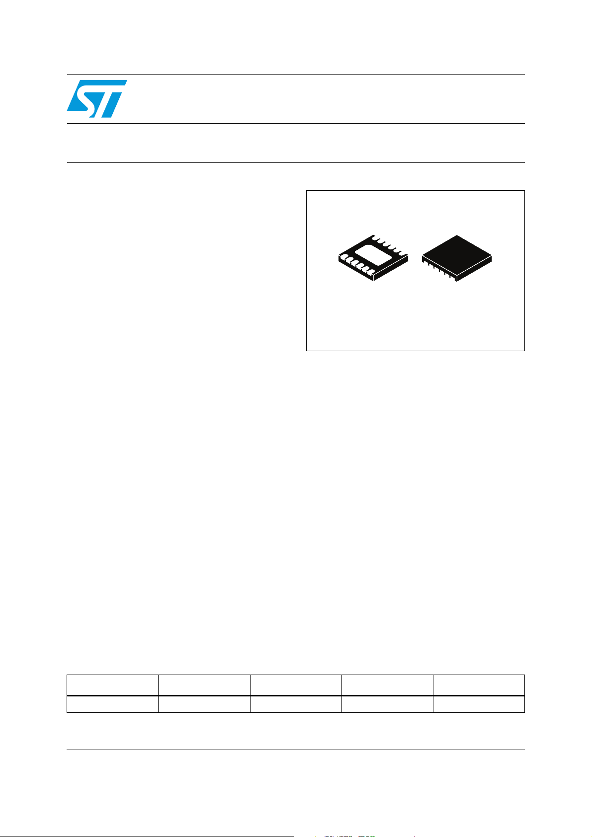
DFN12L (3 x 3 mm)
Description
The STOD03AS is a dual DC-DC converter with
short-circuit protection for AMOLED display
panels. It integrates a step-up and an inverting
DC-DC converter making it particularly suitable
for battery operated products, in which the major
concern is overall system efficiency. It works in
pulse skipping mode during light load conditions
and PWM-MODE at 1.5 MHz frequency for
medium/high load conditions. The high frequency
allows the value and size of external components
to be reduced. The Enable pin allows the device
to be turned off, therefore reducing the current
consumption to less than 1 µA. The negative
output voltage can be programmed by an MCU
through a dedicated pin which implements singlewire protocol. Soft-start with controlled inrush
current limit and thermal shutdown are integrated
functions of the device.
Table 1. Device summary
Order code Positive voltage Negative voltage Package Packaging
STOD03ASTPUR 4.6V -2.4V to -5.4V DFN12L (3 x 3 mm) 3000 parts per reel
December 2011 Doc ID 022614 Rev 1 1/24
www.st.com
24
Page 2

Contents STOD03AS
Contents
1 Schematic . . . . . . . . . . . . . . . . . . . . . . . . . . . . . . . . . . . . . . . . . . . . . . . . . 3
2 Pin configuration . . . . . . . . . . . . . . . . . . . . . . . . . . . . . . . . . . . . . . . . . . . . 5
3 Maximum ratings . . . . . . . . . . . . . . . . . . . . . . . . . . . . . . . . . . . . . . . . . . . . 6
4 Electrical characteristics . . . . . . . . . . . . . . . . . . . . . . . . . . . . . . . . . . . . . 7
5 Typical performance characteristics . . . . . . . . . . . . . . . . . . . . . . . . . . . 10
6 Detailed description . . . . . . . . . . . . . . . . . . . . . . . . . . . . . . . . . . . . . . . . 12
6.1 S
6.1.1 S
6.1.2
6.1.3
. . . . . . . . . . . . . . . . . . . . . . . . . . . . . . . . . . . . . . . . . . . . . . . . . . . . 12
WIRE
features and benefits . . . . . . . . . . . . . . . . . . . . . . . . . . . . . . . . . 12
WIRE
S
S
protocol . . . . . . . . . . . . . . . . . . . . . . . . . . . . . . . . . . . . . . . . . . . 12
WIRE
basic operations . . . . . . . . . . . . . . . . . . . . . . . . . . . . . . . . . . . . . 12
WIRE
6.2 Negative output voltage levels . . . . . . . . . . . . . . . . . . . . . . . . . . . . . . . . . 12
7 Application information . . . . . . . . . . . . . . . . . . . . . . . . . . . . . . . . . . . . . 14
7.1 External passive components . . . . . . . . . . . . . . . . . . . . . . . . . . . . . . . . . 14
7.1.1 Inductor selection . . . . . . . . . . . . . . . . . . . . . . . . . . . . . . . . . . . . . . . . . . 14
7.1.2 Input and output capacitor selection . . . . . . . . . . . . . . . . . . . . . . . . . . . 14
7.2 Recommended PCB layout . . . . . . . . . . . . . . . . . . . . . . . . . . . . . . . . . . . 15
8 Detailed description . . . . . . . . . . . . . . . . . . . . . . . . . . . . . . . . . . . . . . . . 17
8.1 General description . . . . . . . . . . . . . . . . . . . . . . . . . . . . . . . . . . . . . . . . . 17
8.1.1 Multiple operation modes . . . . . . . . . . . . . . . . . . . . . . . . . . . . . . . . . . . . 17
8.1.2 Pulse skipping operation . . . . . . . . . . . . . . . . . . . . . . . . . . . . . . . . . . . . 17
8.1.3 Discontinuous conduction mode . . . . . . . . . . . . . . . . . . . . . . . . . . . . . . 17
8.1.4 Continuous conduction mode . . . . . . . . . . . . . . . . . . . . . . . . . . . . . . . . 17
8.1.5 Enable pin . . . . . . . . . . . . . . . . . . . . . . . . . . . . . . . . . . . . . . . . . . . . . . . 18
8.1.6 Soft-start and inrush current limiting . . . . . . . . . . . . . . . . . . . . . . . . . . . 18
8.1.7 Undervoltage lockout . . . . . . . . . . . . . . . . . . . . . . . . . . . . . . . . . . . . . . . 18
8.1.8 Overtemperature protection . . . . . . . . . . . . . . . . . . . . . . . . . . . . . . . . . . 18
8.1.9 Short-circuit protection . . . . . . . . . . . . . . . . . . . . . . . . . . . . . . . . . . . . . . 18
2/24 Doc ID 022614 Rev 1
Page 3

STOD03AS Contents
8.1.10 Fast discharge . . . . . . . . . . . . . . . . . . . . . . . . . . . . . . . . . . . . . . . . . . . . 18
9 Package mechanical data . . . . . . . . . . . . . . . . . . . . . . . . . . . . . . . . . . . . 20
10 Revision history . . . . . . . . . . . . . . . . . . . . . . . . . . . . . . . . . . . . . . . . . . . 23
Doc ID 022614 Rev 1 3/24
Page 4
Schematic STOD03AS
1 Schematic
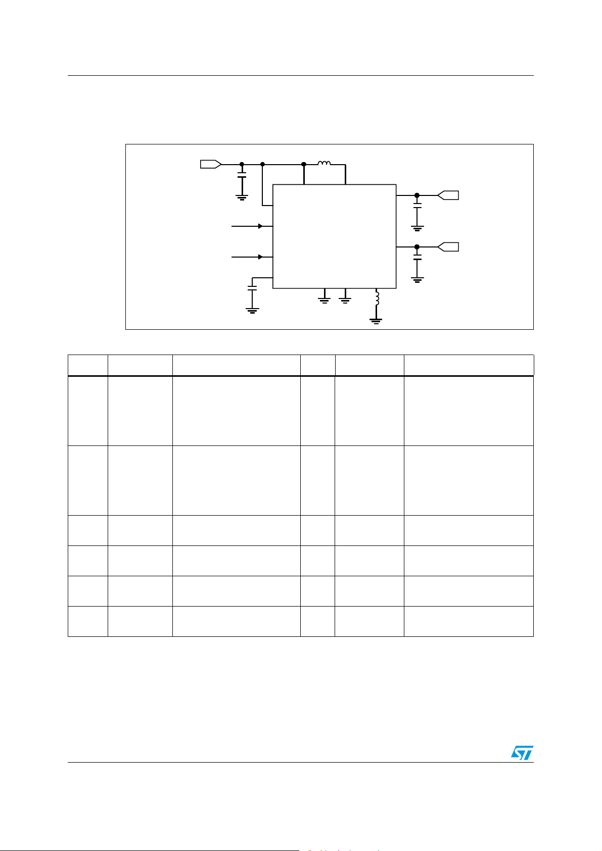
Figure 1. Application schematic
6
"!4
#
).
6
).!
3
%.
6
7)2%
2%&
37IRE
%.
#
2%&
,
6
).0
34/$!3
0'.$ !'.$
,
8
6
-)$
#
-)$
6
/
#
/
,
8
,
!- V
Table 2. Typical external components
Comp. Manufacturer Part number Value Size Ratings
CoilCraft
Murata
(1)
L
1
SEMCO
ABCO
ABCO
CoilCraft
Murata
(2)
L
2
TOKO
ABCO
TDK
C
IN
C
MID
C
O2
C
REF
1. A 200 mA load can be provided with inductor saturation current as a minimum of 0.5 A.
2. At -5.4 V, a 200 mA load can be provided with inductor saturation current as a minimum of 1 A. See Section 7.1.1.
Murata
Taiyo Yuden
Murata
Taiyo Yuden
Murata
Taiyo Yuden
Murata
Taiyo Yuden
LPS4012-472ML
LQH3NPN4R7MJ0
CIG22B4R7MNE
LPF2810T-4R7M
LPF2807T-4R7M
LPS4012-472ML
LQH3NPN4R7MJ0
DFE252012C1239AS-H4R7N
LPF3510T-4R7M
VLF4014AT-4R7M1R1
GRM219R61A106KE44
LMK212BJ106KD-T
GRM219R61A106KE44
LMK212BJ106KD-T
GRM219R61A106KE44
LMK212BJ106KD-T
GRM185R60J105KE26
JMK107BJ105KK-T
4.7µH
4.7µH
2 x
10µF
10µF
2 x
10µF
1µF
4.0 x 4.0 x 1.2
3.0 x 3.0 x 1.1
2.5 x 2.0 x 1.0
2.8 x 2.8 x 1.0
2.8 x 2.8 x 0.7
4.0 x 4.0 x 1.2
3.0 x 3.0 x 1.1
2.5 x 2.0 x 1.2
3.5 x 3.5 x 1.0
3.7 x 3.5 x 1.4
0805
0805
0805
0805
0805
0805
0603
0603
±20%, I = 1.7 A, R = 0.175Ω
±20%, I = 1.1 A, R = 0.156Ω
±20%, I = 1.1 A, R = 0.300Ω
±20%, I = 0.85 A, R = 0.33Ω
±20%, I = 0.70 A, R = 0.44Ω
±20%, I = 1.7 A, R = 0.175Ω
±20%, I = 1.1 A, R = 0.156Ω
±30%, I = 1.2 A, R = 0.252Ω
±20%, I = 0.83 A, R = 0.25Ω
±20%, I = 1.1 A, R = 0.140Ω
±10%, X5R, 10V
±10%, X5R, 10V
±10%, X5R, 10V
±10%, X5R, 10V
±10%, X5R, 10V
±10%, X5R, 10V
±10%, X5R, 6.3V
±10%, X5R, 6.3V
Note: All the above components refer to the typical application performance characteristics.
Operation of the device is not limited to the choice of these external components. Inductor
values ranging from 3.3 µH to 6.8 µH can be used together with the STOD03AS.
4/24 Doc ID 022614 Rev 1
Page 5
STOD03AS Schematic
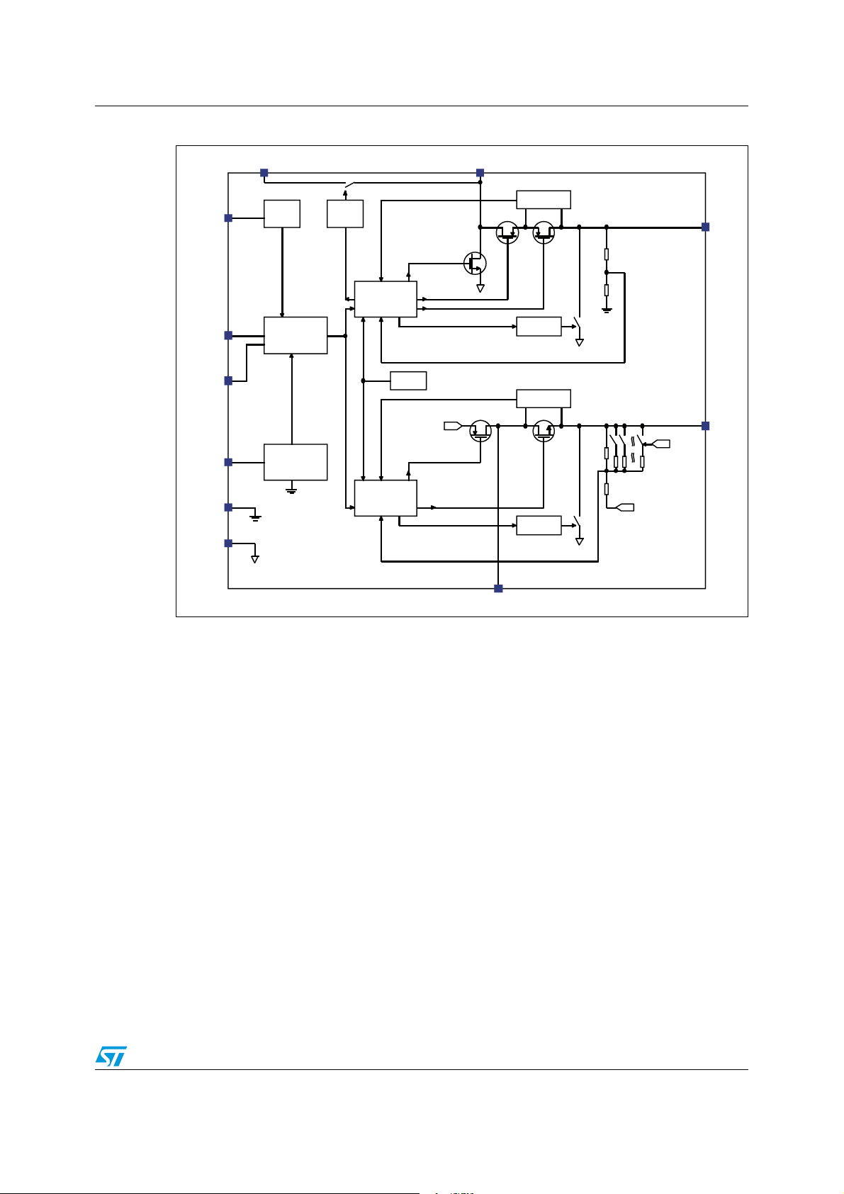
Figure 2. Block schematic
6
).0
,
8
6
).!
%.
3
7)2%
6
2%&
!'.$
0'.$
56,/
,/')##/.42/,
/40
37)2%
62%&
2).'
+),,%2
34%050
#/.42/,
).6%24).'
#/.42/,
/3#
6).0
$-$
6
-)$
0!
0"
.
&!3 4
$)3#(!2'%
$-$
6
0
.
3WIRE
CONTROL
62%&
&!3 4
$)3#(!2'%
,
8
/
!-V
Doc ID 022614 Rev 1 5/24
Page 6

Pin configuration STOD03AS
2 Pin configuration
Figure 3. Pin configuration (top view)
Table 3. Pin description
Pin name Pin n° Description
Lx
1
1 Switching node of the step-up converter
PGND 2 Power ground pin
V
MID
3 Step-up converter output voltage (4.6V)
NC 4 Not internally connected
AGND 5 Signal ground pin. This pin must be connected to the power ground pin
Voltage reference output. 1µF bypass capacitor must be connected
V
REF
S
WIRE
EN 8
V
O2
Lx
2
V
IN A
V
iN P
6
between this pin and AGND
7 Negative voltage setting pin
Enable control pin. ON = V
. When pulled low it puts the device in
INA
shutdown mode
9 Inverting converter output voltage (Default - 4.9V)
10 Switching node of the inverting converter
11 Analogic input supply voltage
12 Power input supply voltage
Exposed
pad
Internally connected to AGND. Exposed pad must be connected to AGND
and PGND in the PCB layout in order to guarantee proper operation of the
device
6/24 Doc ID 022614 Rev 1
Page 7

STOD03AS Maximum ratings
3 Maximum ratings
Table 4. Absolute maximum ratings
Symbol Parameter Value Unit
V
INA
EN, S
IL
L
V
V
L
IL
V
P
T
, V
X2
X2
O2
MID
X1
X1
REF
D
STG
T
J
WIRE
DC supply voltage -0.3 to 6 V
INP
Logic input pins -0.3 to 4.6 V
Inverting converter switching current Internally limited A
Inverting converter switching node voltage - 10 to V
+ 0.3 V
INP
Inverting converter output voltage - 10 to AGND + 0.3 V
Step-up converter and LDO output voltage -0.3 to 6 V
Step-up converter switching node voltage -0.3 to V
+ 0.3 V
MID
Step-up converter switching current Internally limited A
Reference voltage -0.3 to 3 V
Power dissipation Internally limited mW
Storage temperature range -65 to 150 °C
Maximum junction temperature 150 °C
ESD ESD protection HBM 2 kV
Note: Absolute maximum ratings are those values beyond which damage to the device may occur.
Functional operation under these conditions is not implied.
Table 5. Thermal data
Symbol Parameter Value Unit
R
thJA
R
thJC
1. The package is mounted on a 4-layer (2S2P) JEDEC board as per JESD51-7.
Thermal resistance junction-ambient 33 °C/W
Thermal resistance junction-case (FR-4 PCB)
(1)
2.12 °C/W
Doc ID 022614 Rev 1 7/24
Page 8
Electrical characteristics STOD03AS
4 Electrical characteristics
TJ = 25 °C, V
C
= 2 x 10 µF, C
O2
INA
= V
= 3.7 V, I
INP
= 1 µF, L1 = L2 = 4.7 µH, V
REF
MID,O2
= 30 mA, C
= 2 x 10 µF, C
IN
= 2 V, V
EN
= 10 µF,
MID
= 4.6 V, VO2= -4.9 V unless
MID
otherwise specified.
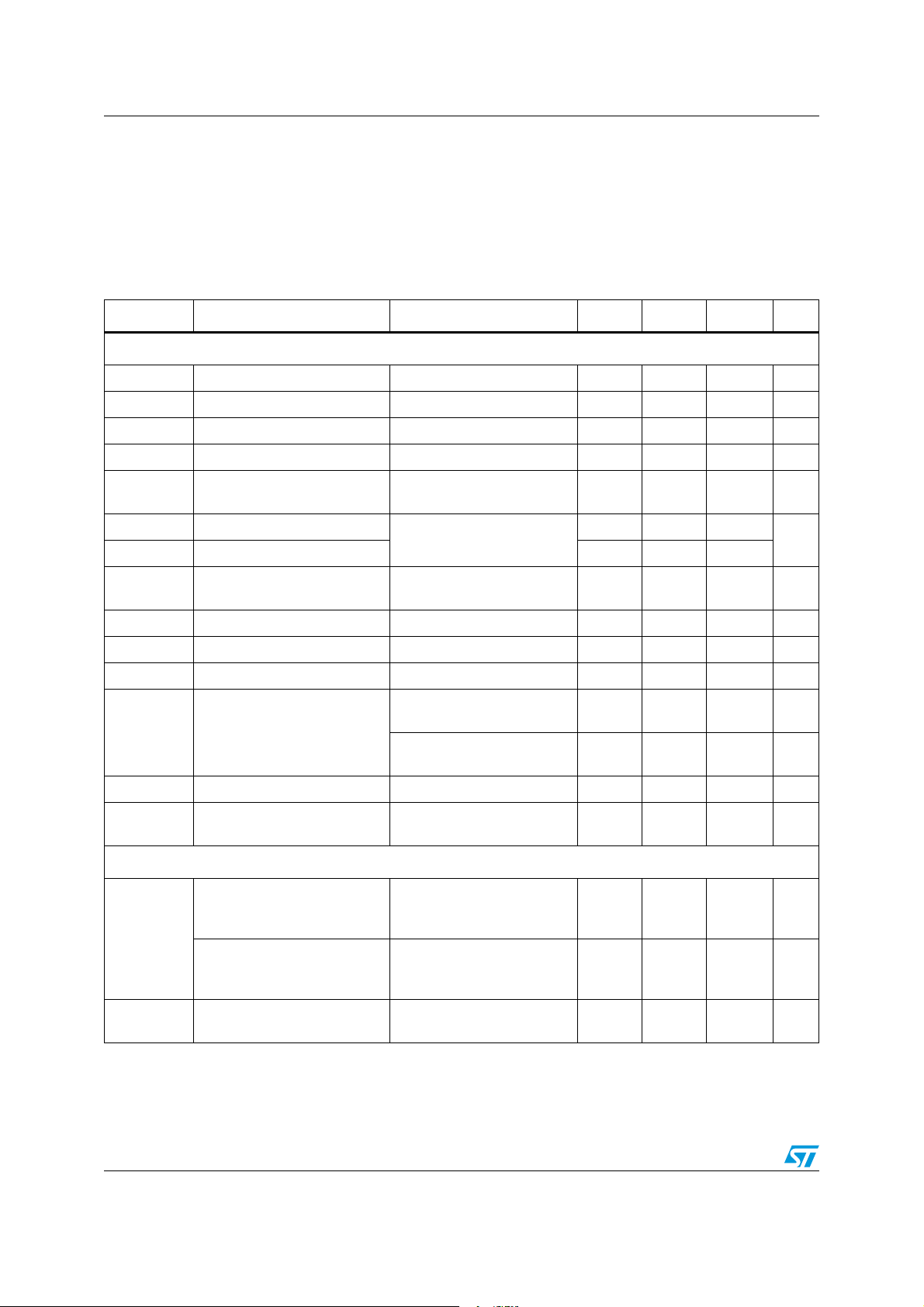
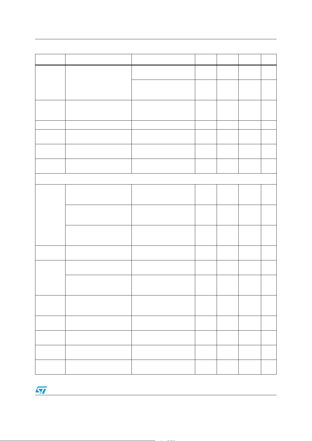
Table 6. Electrical characteristics
Symbol Parameter Test conditions Min. Typ. Max. Unit
General section
V
INA, VINP
UVLO_H Undervoltage lockout HIGH V
UVLO_L Undervoltage lockout LOW V
I_V
I
Q_SH
V
EN
V
EN
I
EN
f
D1
D2
η Total system efficiency
V
REF
I
REF
Supply input voltage 2.3 3.7 4.5 V
rising 2.22 2.25 V
INA
falling 1.9 2.18 V
INA
Input current No load condition 1.7 2.1 mA
I
=GND
V
Shutdown current
H Enable high threshold
L Enable low threshold 0.4
Enable input current
S
MAX
MAX
Switching frequency PWM mode 1.2 1.5 1.7 MHz
Step-up maximum duty cycle No load 87 %
Inverting maximum duty cycle No load 87 %
Voltage reference I
Voltage reference current
capability
EN
TJ=-40°C to +85°C
V
=2.5V to 4.5V,
INA
1.2
TJ=-40°C to +85°C
V
EN=VINA
=-40°C to +85°C
T
J
I
MID,O2
V
MID
I
MID,O2
V
MID
REF
At 98.5% of no load
reference voltage
=4.5V
=10 to 30mA,
=4.6V, VO2=-4.9V
=30 to 150mA,
=4.6V, VO2=-4.9V
80 %
85 %
=10µA 1.216 1.228 1.240 V
100 µA
1µA
1µA
V
Step-up converter section
Positive voltage total variation
V
INA=VINP
I
MID
=2.5V to 4.5V;
=5mA to 150mA, IO2 no
load, TJ=25°C
V
MID
Temperature accuracy
V
INA=VINP
I
O2
=3.7V; I
no load; TJ=-40°C to
MID
+85°C
=3.5V to 3.0V,
V
ΔV
MID LT
Line transient
INA,P
=100mA; TR=TF=50µs
I
MID
8/24 Doc ID 022614 Rev 1
4.55 4.6 4.65 V
=5mA;
±0.5 %
-12 mV
Page 9
STOD03AS Electrical characteristics
Table 6. Electrical characteristics (continued)
Symbol Parameter Test conditions Min. Typ. Max. Unit
I
ΔV
MIDT
V
MID-PP
I
MID MAX
I-L
1MAX
R
DSON
Load transient regulation
TDMA noise line transient
regulation
Max. step-up load current V
Step-up inductor peak current
P-channel static drain-source
P1
ON resistance
=3 to 30mA and I
MID
to 3mA, T
=10 to 100mA and
I
MID
I
=100 to 10mA,
MID
=30µs
T
R=TF
=5 to 100mA; V
I
MID
R=TF
=30µs
=2.9V to 3.4V; F=200Hz;
=50µs; IO2 no load
T
R=TF
=2.9V to 4.5V 200 mA
INA,P
10% below of nominal
V
MID
value
V
=3.7V, ISW=100mA 1.0 2.0 Ω
INA,P
MID
INA,P
=30
±20 mV
±25 mV
±20 mV
0.9 1.1 A
R
DSON
N-channel static drain-source
N1
ON resistance
Inverting converter section
Output negative voltage range
V
O2
Output negative voltage total
variation on default value
Temperature accuracy
ΔV
O2 LT
Line transient
Load transient regulation
ΔV
O2T
Load transient regulation
V
O2-PP
I
O2
TDMA noise line transient
regulation
Maximum inverting output
current
V
=3.7V, ISW=100mA 0.4 1.0 Ω
INA,P
31 different values set by the
S
WIRE
pin
-5.4 -2.4 V
(see Section 6.1.2)
V
INA=VINP
IO2=5mA to 150mA, I
=2.5V to 4.5V;
MID
no
-4.97 -4.9 -4.83 V
load, TJ=25°C
V
INA=VINP
I
MID
=3.7V; IO2=5mA,
no load,
±0.5 %
TJ=-40°C to +85°C
V
=3.5V to 3.0V,
INA,P
IO2=100mA, TR=TF=50µs
=3 to 30mA and IO2=30 to
I
O2
3mA, T
=10 to 100mA and
I
O2
=100 to 10mA,
I
O2
T
R=TF
=5 to 100mA; V
I
O2
R=TF
=100µs
=100µs
INA,P
=2.9V to 3.4V; F=200Hz;
=50µs; I
T
R=TF
V
=2.9V to 4.5V -200 mA
INA,P
MID
no load
+12 mV
±20 mV
±25 mV
±25 mV
R
R
I-L
2MAX
DSON
DSON
Inverting peak current
P-channel static drain-source
P2
ON resistance
N-channel static drain-source
N2
ON resistance
V
below 10% of nominal
O2
value
=3.7V, ISW=100mA 0.42 Ω
V
INA,P
V
=3.7V, ISW=100mA 0.43 Ω
INA,P
-1.2 -0.9 A
Doc ID 022614 Rev 1 9/24
Page 10

Electrical characteristics STOD03AS
Table 6. Electrical characteristics (continued)
Symbol Parameter Test conditions Min. Typ. Max. Unit
Thermal shutdown
OTP Overtemperature protection 140 °C
OTP
HYST
Overtemperature protection
hysteresis
Discharge resistor
R
DIS
T
DIS
Resistor value No load 400 Ω
Discharge time
No load, V
MID-VO2
nominal value
at 10% of
15 °C
8ms
10/24 Doc ID 022614 Rev 1
Page 11
STOD03AS Typical performance characteristics
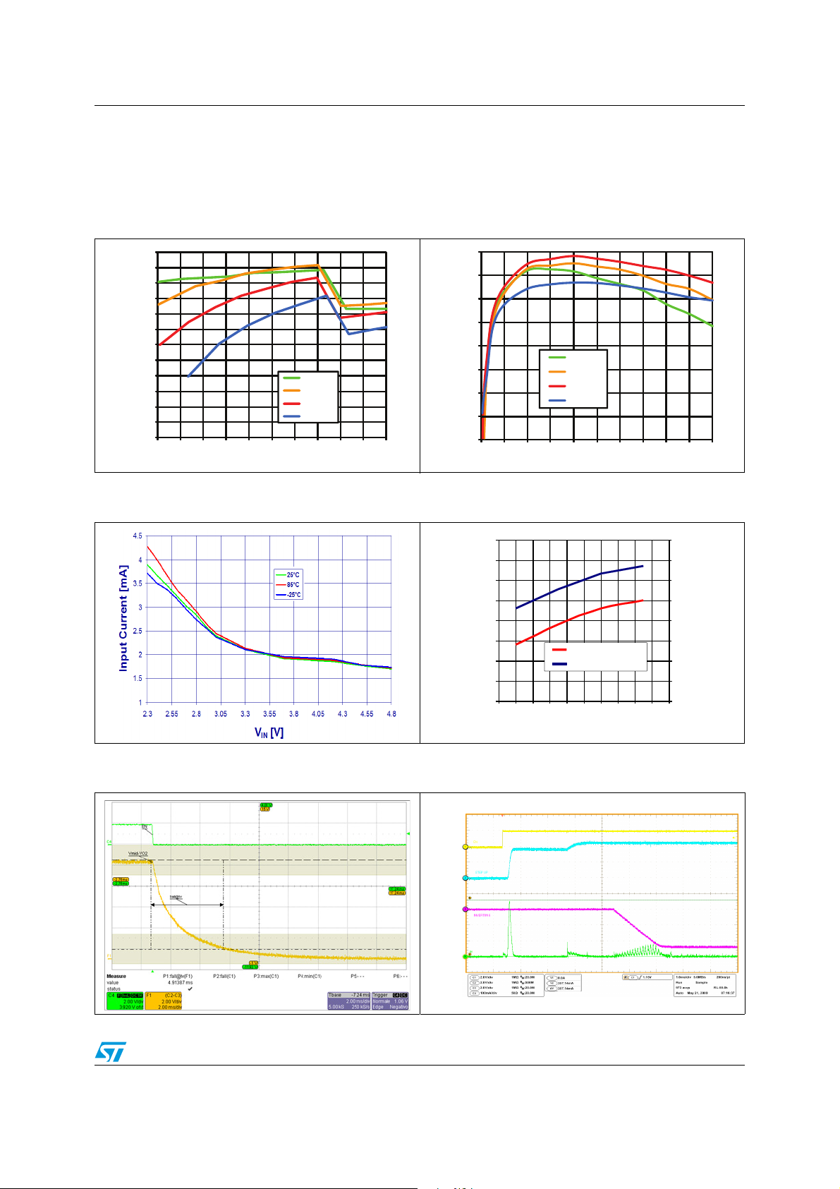
5 Typical performance characteristics
V
= - 4.9 V; TA = 25 °C; See Ta bl e 1 for external components used in the tests below.
O2
Figure 4. Efficiency vs. input voltage Figure 5. Efficiency vs. output current
Efficiency [%]
90%
88%
86%
84%
82%
80%
78%
76%
74%
72%
70%
68%
66%
2.5 2.7 2.9 3.1 3.33.5 3.7 3.9 4.1 4.3 4.5
Io=50mA
Io=100mA
Io=150mA
Io=200mA
VIN[V]
90%
85%
80%
75%
70%
Efficiency [%]
65%
60%
55%
50%
020406080 100 120 140 160 180200
VIN=2.7V
VIN=3.2V
VIN=3.7V
VIN=4.2V
I
OUT
[mA]
Figure 6. Input current vs. VIN no load Figure 7. Max. power output vs. V
Figure 8. Fast discharge V
= 3.7 V, no load Figure 9. Startup and inrush V
IN
V
EN
MID
TA = 25 °C
500
450
400
350
[mA]
300
OUT
I
250
200
max I
max P
OUT
OUT
at V
O2
150
100
2.5 2.7 2.9 3.1 3.3 3.5 3.7 3.9 4.1 4.3 4.5
VIN[V]
load
= -4.9V
IN
IN,
4.0
3.5
3.0
2.5
[W]
2.0
OUT
P
1.5
1.0
0.5
0.0
= 3.7 V, no
V
O2
I
IN
Doc ID 022614 Rev 1 11/24
Page 12
Typical performance characteristics STOD03AS
INA
= V
= 3.7 V, I
INP
= 100 mA, TA = 25 °C
MID
VEN = V
INA
= V
= 3.7 V, IO2 = 100 mA, TA = 25 °C
INP
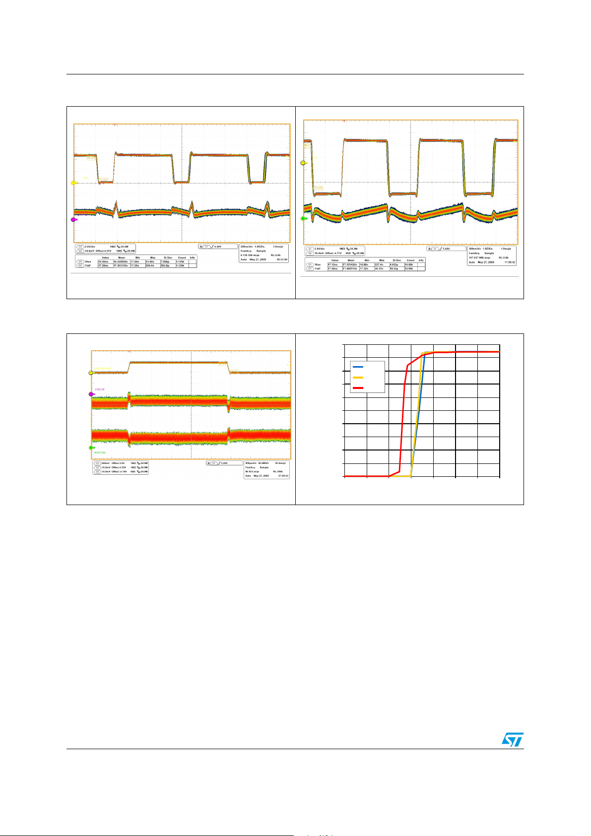
Figure 10. Step-up CCM operation Figure 11. Inverting CCM operation
VEN = V
Figure 12. Line transient Figure 13. Output voltage vs. input voltage
I
= 200 mA, V
O
10.00
9.00
V
IN
8.00
7.00
V
MID
[V]
+V
V
6.00
O2
5.00
O1
4.00
-40 °C
25 °C
85 °C
3.00
V
O2
2.00
1.00
0.00
1.6 1.8 2 2.2 2.4 2.6 2.8 3
V
= V
INA
= 2.9 to 3.4 V, I
INP
= 100 mA, TR = TF = 50 µs
MID,O2
O2
V
IN
= - 4.9 V
[V]
12/24 Doc ID 022614 Rev 1
Page 13

STOD03AS Detailed description
6 Detailed description
6.1 S
● Protocol: to digitally communicate over a single cable with single-wire components
● Single-wire's 3 components:
1. an external MCU
2. wiring and associated connectors
3. the STOD03AS device with a dedicated single-wire pin.
6.1.1 S
● Fully digital signal
● No handshake needed
● Protection against glitches and spikes though an internal low pass filter acting on falling
● Uses a single wire (plus analog ground) to accomplish both communication and power
● Simplified design with an interface protocol that supplies control and signaling over a
6.1.2 S
● Single-wire protocol uses conventional CMOS/TTL logic levels (maximum 0.6 V for
● Both master (MCU) and slave (STOD03AS) are configured to permit bit sequential data
● Data is bit-sequential with a START bit and a STOP bit
● Signal is transferred in real time
● System clock is not required; each single-wire pulse is self-clocked by the oscillator
WIRE
features and benefits
WIRE
edges
control transmission
single-wire connection to set the output voltages.
protocol
WIRE
logic “zero” and a minimum 1.2 V for logic “one”) with operation specified over a supply
voltage range of 2.5 V to 4.5 V
to flow only in one direction at a time; master initiates and controls the device
integrated in the master and is asserted valid within a frequency range of 250 kHz
(maximum).
6.1.3 S
basic operations
WIRE
● The negative output voltage levels are selectable within a wide range (steps of 100 mV)
● The device can be enabled / disabled via S
Doc ID 022614 Rev 1 13/24
in combination with the Enable pin.
WIRE
Page 14
Detailed description STOD03AS
6.2 Negative output voltage levels
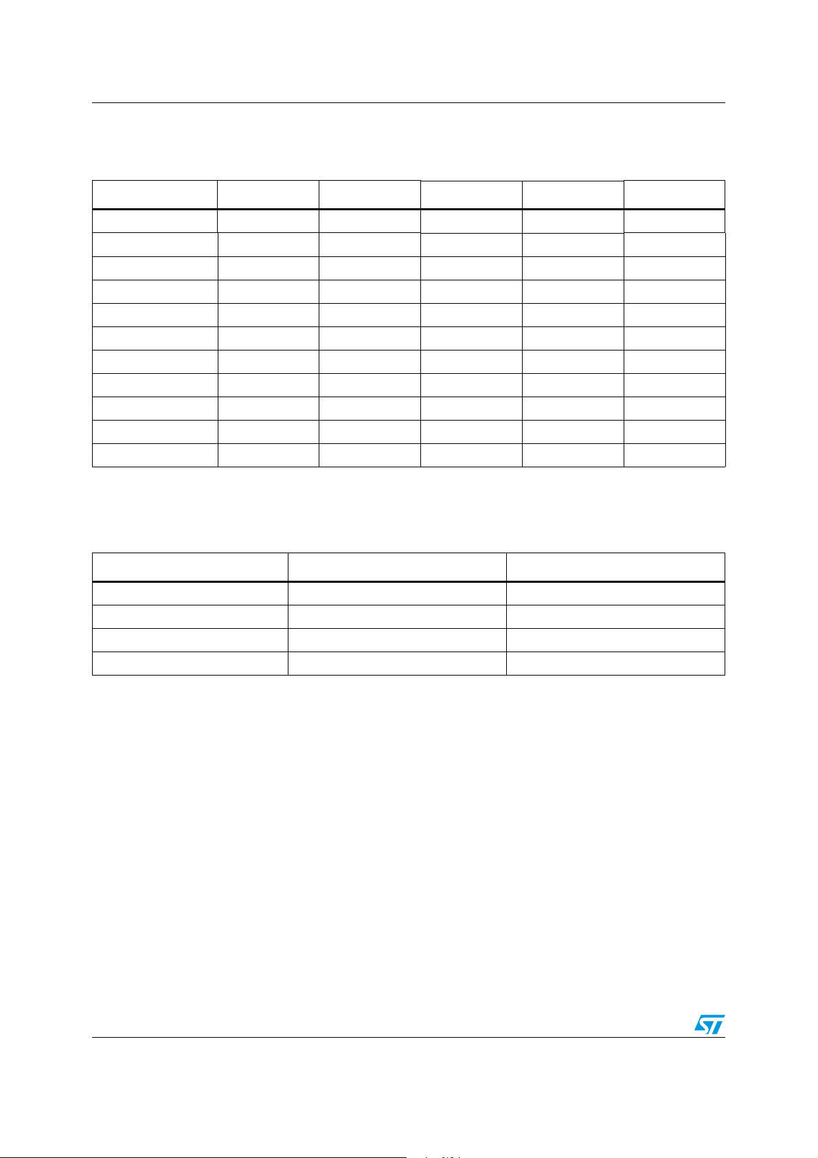
Table 7. Negative output voltage levels
Pulse V
O2
Pulse V
1 -5.411-4.421-3.4
2 -5.312-4.322-3.3
3 -5.213-4.223-3.2
4 -5.114-4.124-3.1
5 -5.015-4.025-3.0
(1)
6
-4.9 16 -3.9 26 -2.9
7 -4.817-3.827-2.8
8 -4.718-3.728-2.7
9 -4.619-3.629-2.6
10 -4.5 20 -3.5 30 -2.5
1. Default output voltage.
Table 8. Enable and S
operation table
WIRE
Enable S
Low Low Device off
(1)
WIRE
O2
Pulse V
31 -2.4
Action
O2
Low High Negative output set by S
High Low Default negative output voltage
High High Default negative output voltage
1. The Enable pin must be set to AGND while using the S
WIRE
WIRE
function.
14/24 Doc ID 022614 Rev 1
Page 15

STOD03AS Application information
7 Application information
7.1 External passive components
7.1.1 Inductor selection
Magnetic shielded low ESR power inductors must be chosen as the key passive
components for switching converters.
For the step-up converter an inductance between 4.7 µH and 6.8 µH is recommended.
For the inverting stage the suggested inductance ranges from 3.3 µH to 4.7 µH.
It is very important to select the right inductor according to the maximum current the
inductor can handle to avoid saturation. The step-up and the inverting peak current can be
calculated as follows:
Equation 1
IV
×
I
−
=
BOOSTPEAK
OUTMID
VIN1
×η
+
MIN
MID
−×
×××
)VINV(VIN
MINMIDMIN
1LfsV2
Equation 2
x-
x-
)2(
IVOVIN
)2(
MIN
MIN
IVOVIN
=
I
I
-
-
INVERTINGPEAK
INVERTINGPEAK
=
x
x
η
η
2
VIN
2
VIN
where
V
: step-up output voltage, fixed at 4.6 V;
MID
V
: inverting output voltage including sign (minimum value is the absolute maximum
O2
value);
I
: output current for both DC-DC converters;
O
V
: input voltage for the STOD03AS;
IN
f
: switching frequency. Use the minimum value of 1.2 MHz for the worst case;
s
η1: efficiency of step-up converter. Typical value is 0.85;
η2: efficiency of inverting converter. Typical value is 0.75.
The negative output voltage can be set via S
WIRE
current, at the maximum load condition, increases. A proper inductor, with a saturation
current as a minimum of 1 A, is preferred.
7.1.2 Input and output capacitor selection
x
x
2
VOVIN
2
VOVIN
OUTMINMIN
OUTMINMIN
+
+
x
x
MINMIN
MINMIN
xx-
xx-
2)2(2
LfsVINVO
2)2(2
MINMIN
MINMIN
LfsVINVO
at - 5.4 V. Accordingly, the inductor peak
It is recommended to use X5R or X7R low ESR ceramic capacitors as input and output
capacitors in order to filter any disturbance present in the input line and to obtain stable
operation for the two switching converters. A minimum real capacitance value of 6 µF must
be guaranteed for C
variation and DC polarization, a 10 µF, 10 V ±10% capacitor as C
±10% as C
, can be used to achieve the required 6 µF.
O2
and CO2 in all conditions. Considering tolerance, temperature
MID
Doc ID 022614 Rev 1 15/24
and 2 x 10 µF, 10 V
MID
Page 16
Application information STOD03AS
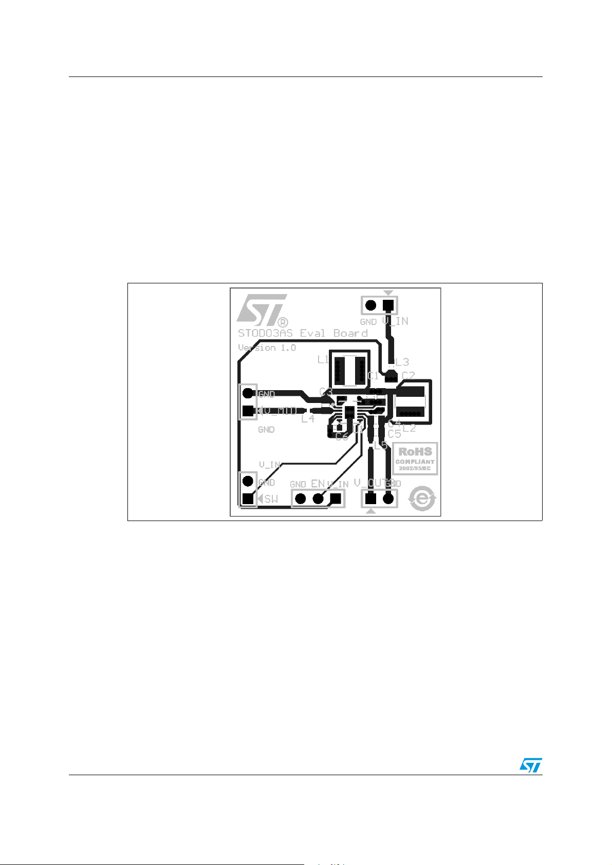
7.2 Recommended PCB layout
The STOD03AS is high frequency power switching device and therefore requires a proper
PCB layout in order to obtain the necessary stability and optimize line/load regulation and
output voltage ripple.
Analog input (V
at the C
pad only. The input capacitor must be as close as possible to the IC.
IN
) and power input (V
INA
) must be kept separated and connected together
INP
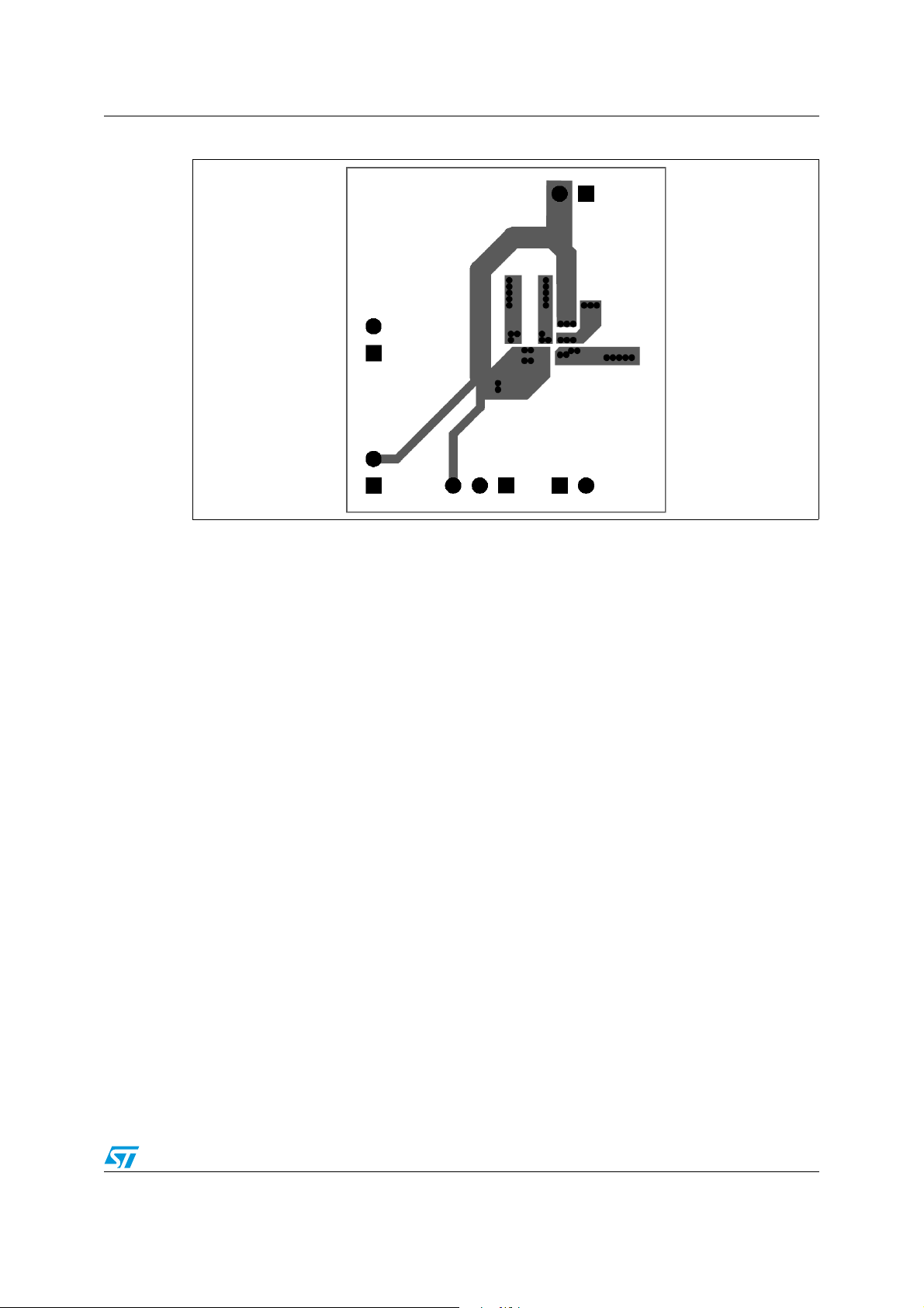
In order to minimize the ground noise, a common ground node for power ground and a
different one for analog ground must be used. In the recommended layout, the AGND node
is placed close to C
ground while the PGND node is centered at CIN ground. They are
REF
connected by a separated layer routing on the bottom through vias.
The exposed pad is connected to AGND through vias.
Figure 14. Top layer and silk-screen (top view, not to scale)
16/24 Doc ID 022614 Rev 1
Page 17
STOD03AS Application information
Figure 15. Bottom layer and silk-screen (top view, not to scale)
Doc ID 022614 Rev 1 17/24
Page 18

Detailed description STOD03AS
8 Detailed description
8.1 General description
The STOD03AS is a high efficiency dual DC-DC converter which integrates a step-up and
inverting power stage suitable for supplying AMOLED panels. Thanks to the high level of
integration it needs only 6 external components to operate and it achieves very high
efficiency using a synchronous rectification technique for each of the two DC-DC converters.
The controller uses an average current mode technique in order to obtain good stability and
precise voltage regulation in all possible conditions of input voltage, output voltage, and
output current. In addition, the peak inductor current is monitored in order to avoid saturation
of the coils.
The STOD03AS implements a power saving technique in order to maintain high efficiency at
very light load and it switches to PWM operation as the load increases in order to guarantee
the best dynamic performances and low noise operation.
The STOD03AS avoids battery leakage thanks to the true-shutdown feature and it is self
protected from overtemperature. Undervoltage lockout and soft-start guarantee proper
operation during startup.
8.1.1 Multiple operation modes
Both the step-up and the inverting stage of the STOD03AS operate in three different modes:
pulse skipping (PS), discontinuous conduction mode (DCM) and continuous conduction
mode (CCM). It switches automatically between the three modes according to input voltage,
output current, and output voltage conditions.
8.1.2 Pulse skipping operation
The STOD03AS works in pulse skipping mode when the load current is below some tens of
mA. The load current level at which this way of operation occurs depends on input voltage
only for the step-up converter and on input voltage and negative output voltage (V
inverting converter.
8.1.3 Discontinuous conduction mode
When the load increases above a few mA, the STOD03AS enters DCM operation. In order
to obtain this type of operation the controller must avoid the inductor current going negative.
The discontinuous mode detector (DMD) blocks sense the voltage across the synchronous
rectifiers (P1B for the step-up and N2 for the inverting) and turn off the switches when the
voltage crosses a defined threshold which, in turn, represents a certain current in the
inductor. This current can vary according to the slope of the inductor current which depends
on input voltage, inductance value, and output voltage.
8.1.4 Continuous conduction mode
) for the
O2
At medium/high output loads, the STOD03AS enters full CCM at constant switching
frequency mode for each of the two DC-DC converters.
18/24 Doc ID 022614 Rev 1
Page 19

STOD03AS Detailed description
8.1.5 Enable pin
The device operates when the EN pin is set high. If the EN pin is set low, the device stops
switching, and all the internal blocks are turned off. In this condition the current drawn from
V
INP/VINA
is below 1 µA in the whole temperature range. In addition, the internal switches
are in an OFF state so the load is electrically disconnected from the input, this avoids
unwanted current leakage from the input to the load.
When the EN is pulled high, the P1B switch is turned on for 100 µs. In normal operation,
during this time, apart of a small drop due to parasitic resistance, V
If, after this 100 µs, V
stays below VIN, the P1B is turned off and stays off until a new
MID
reaches VIN.
MID
pulse is applied to the EN. This mechanism avoids the STOD03AS starting if a short-circuit
is present on V
MID
.
8.1.6 Soft-start and inrush current limiting
After the EN pin is pulled high, or after a suitable voltage is applied to V
device initiates the startup phase.
As a first step, the C
capacitor is charged and the P1B switch implements a current
MID
limiting technique in order to keep the charge current below 400 mA. This avoids the battery
overloading during startup.
After V
reaches the V
MID
voltage level, the P1B switch is fully turned on and the soft-start
INP
procedure for the step-up is started. After around 2 ms the soft-start for the inverting is
started. The positive and negative voltages are under regulation at around 6 ms after the
EN pin is asserted high.
8.1.7 Undervoltage lockout
The undervoltage lockout function avoids improper operation of the STOD03AS when the
input voltage is not high enough. When the input voltage is below the UVLO threshold the
device is in shutdown mode. The hysteresis of 50mV avoids unstable operation when the
input voltage is close to the UVLO threshold.
8.1.8 Overtemperature protection
An internal temperature sensor continuously monitors the IC junction temperature. If the IC
temperature exceeds 140 °C, typical, the device stops operating. As soon as the
temperature falls below 125 °C, typical, normal operation is restored.
8.1.9 Short-circuit protection
INP
, V
INA
and EN, the
When short-circuit occurs, the device is able to detect the voltage difference between VIN
and V
. Overshoots on LX1 are limited, decreasing the inductor current. After that, the
MID
output stages of the device are turned off. This status is maintained, avoiding current flowing
to the load. A new ENABLE transition is needed to restart the device. During startup the
short-circuit protection is active.
8.1.10 Fast discharge
When ENABLE turns from high to low level, the device goes into shutdown mode and LX1
and LX2 stop switching. Then, the discharge switch between V
between V
output voltage. When the output voltages are discharged to 0 V, the switches turn off and the
outputs are high impedance.
and GND turn on and discharge the positive output voltage and negative
O2
and VIN and the switch
MID
Doc ID 022614 Rev 1 19/24
Page 20

Package mechanical data STOD03AS
9 Package mechanical data
In order to meet environmental requirements, ST offers these devices in different grades of
ECOPACK
specifications, grade definitions and product status are available at:
is an ST trademark.
®
packages, depending on their level of environmental compliance. ECOPACK
www.st.com. ECOPACK
20/24 Doc ID 022614 Rev 1
Page 21
STOD03AS Package mechanical data
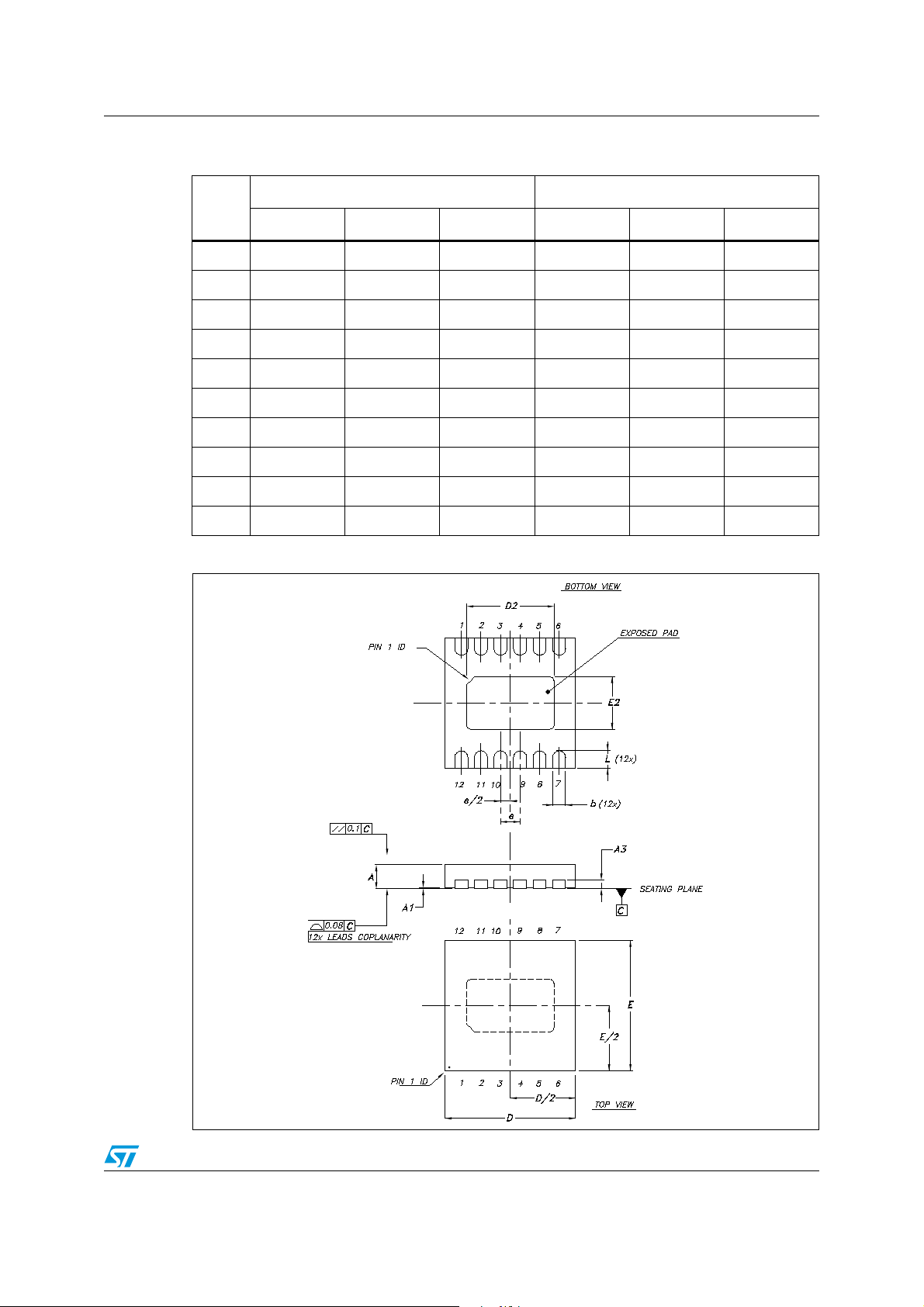
Table 9. DFN12L (3 x 3) mechanical data
mm. inch.
Dim.
Min. Typ. Max. Min. Typ. Typ.
A 0.51 0.55 0.60 0.020 0.022 0.024
A1 0 0.02 0.05 0 0.001 0.002
A3 0.20 0.008
b 0.18 0.25 0.30 0.007 0.010 0.012
D 2.85 3 3.15 0.112 0.118 0.124
D2 1.87 2.02 2.12 0.074 0.080 0.083
E 2.85 3 3.15 0.112 0.118 0.124
E2 1.06 1.21 1.31 0.042 0.048 0.052
e 0.45 0.018
L 0.30 0.40 0.50 0.012 0.016 0.020
Figure 16. DFN12L (3 x 3) drawing
8085116-A
Doc ID 022614 Rev 1 21/24
Page 22
Package mechanical data STOD03AS
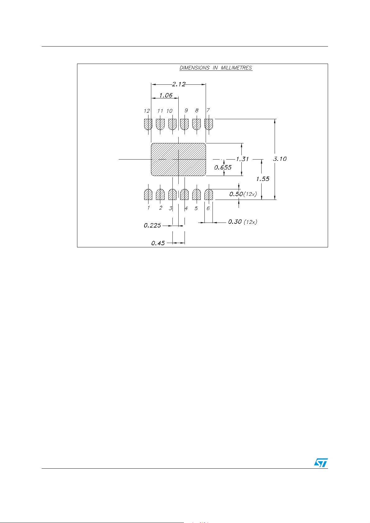
Figure 17. DFN12L (3 x 3 mm) footprint recommended data
22/24 Doc ID 022614 Rev 1
Page 23

STOD03AS Revision history
10 Revision history
Table 10. Document revision history
Date Revision Changes
20-Dec-2011 1 Initial release.
Doc ID 022614 Rev 1 23/24
Page 24

STOD03AS
Please Read Carefully:
Information in this document is provided solely in connection with ST products. STMicroelectronics NV and its subsidiaries (“ST”) reserve the
right to make changes, corrections, modifications or improvements, to this document, and the products and services described herein at any
time, without notice.
All ST products are sold pursuant to ST’s terms and conditions of sale.
Purchasers are solely responsible for the choice, selection and use of the ST products and services described herein, and ST assumes no
liability whatsoever relating to the choice, selection or use of the ST products and services described herein.
No license, express or implied, by estoppel or otherwise, to any intellectual property rights is granted under this document. If any part of this
document refers to any third party products or services it shall not be deemed a license grant by ST for the use of such third party products
or services, or any intellectual property contained therein or considered as a warranty covering the use in any manner whatsoever of such
third party products or services or any intellectual property contained therein.
UNLESS OTHERWISE SET FORTH IN ST’S TERMS AND CONDITIONS OF SALE ST DISCLAIMS ANY EXPRESS OR IMPLIED
WARRANTY WITH RESPECT TO THE USE AND/OR SALE OF ST PRODUCTS INCLUDING WITHOUT LIMITATION IMPLIED
WARRANTIES OF MERCHANTABILITY, FITNESS FOR A PARTICULAR PURPOSE (AND THEIR EQUIVALENTS UNDER THE LAWS
OF ANY JURISDICTION), OR INFRINGEMENT OF ANY PATENT, COPYRIGHT OR OTHER INTELLECTUAL PROPERTY RIGHT.
UNLESS EXPRESSLY APPROVED IN WRITING BY TWO AUTHORIZED ST REPRESENTATIVES, ST PRODUCTS ARE NOT
RECOMMENDED, AUTHORIZED OR WARRANTED FOR USE IN MILITARY, AIR CRAFT, SPACE, LIFE SAVING, OR LIFE SUSTAINING
APPLICATIONS, NOR IN PRODUCTS OR SYSTEMS WHERE FAILURE OR MALFUNCTION MAY RESULT IN PERSONAL INJURY,
DEATH, OR SEVERE PROPERTY OR ENVIRONMENTAL DAMAGE. ST PRODUCTS WHICH ARE NOT SPECIFIED AS "AUTOMOTIVE
GRADE" MAY ONLY BE USED IN AUTOMOTIVE APPLICATIONS AT USER’S OWN RISK.
Resale of ST products with provisions different from the statements and/or technical features set forth in this document shall immediately void
any warranty granted by ST for the ST product or service described herein and shall not create or extend in any manner whatsoever, any
liability of ST.
ST and the ST logo are trademarks or registered trademarks of ST in various countries.
Information in this document supersedes and replaces all information previously supplied.
The ST logo is a registered trademark of STMicroelectronics. All other names are the property of their respective owners.
© 2011 STMicroelectronics - All rights reserved
STMicroelectronics group of companies
Australia - Belgium - Brazil - Canada - China - Czech Republic - Finland - France - Germany - Hong Kong - India - Israel - Italy - Japan -
Malaysia - Malta - Morocco - Philippines - Singapore - Spain - Sweden - Switzerland - United Kingdom - United States of America
www.st.com
24/24 Doc ID 022614 Rev 1
 Loading...