

Page 1
DIGITAL CELLULAR APPLICATIONS
■ LINEARPOWER AMPLIFIER
■ 915-960MHz
■ 26 VOLTS
■ INPUT/OUTPUT50 OHMS
■ POUT = 42 dBm CW or PEP
■ GAIN = 30 dB
DESCRIPTION
The STM961-15B module is designed for digital
cellular radio base station applications in the
915-960 MHz frequencyrangeoperatingat 26V.
The STM961-15B is designed to meet the low
distortion, high linearity requirements of modern
digital cellular base station equipment.
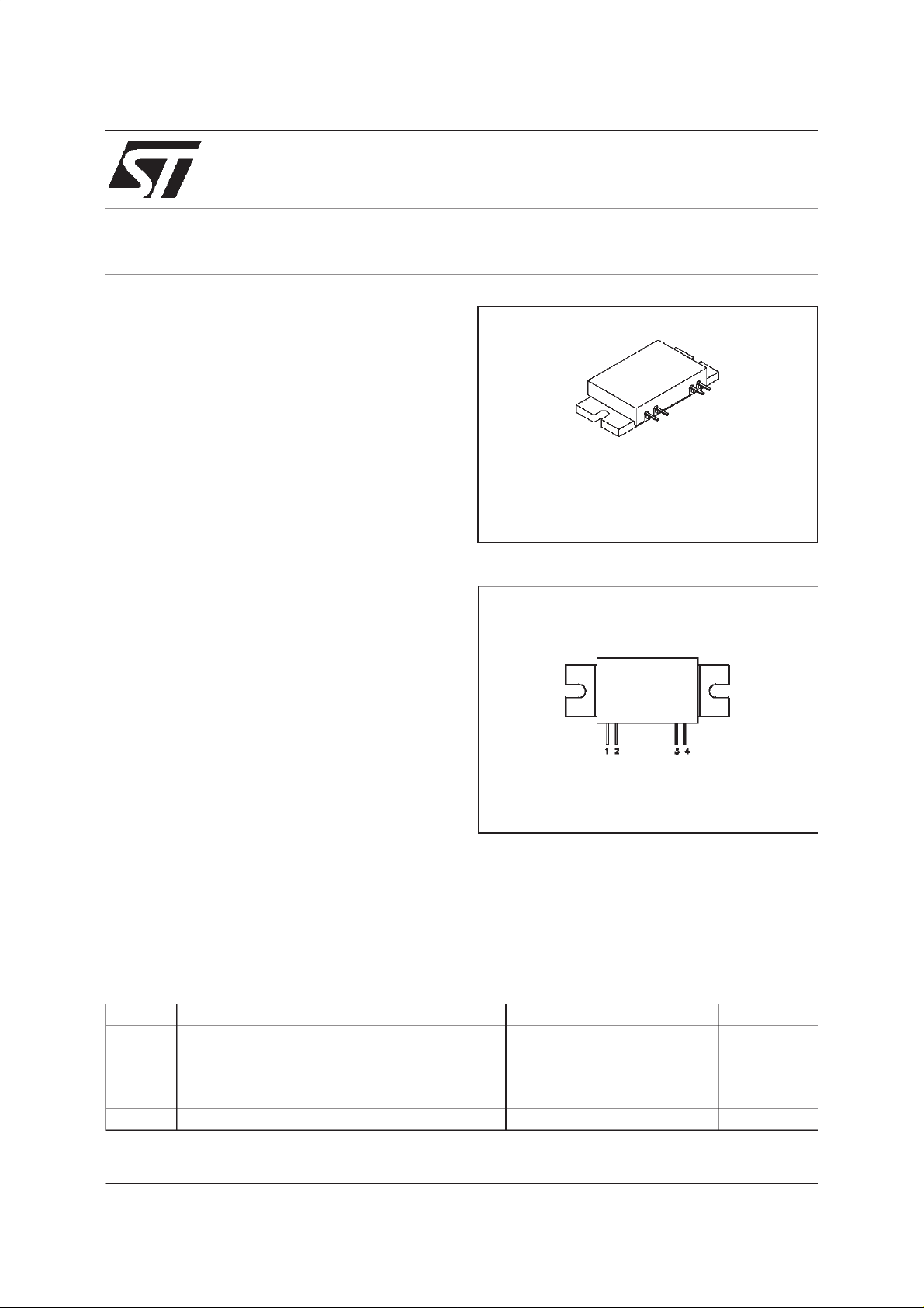
STM961-15B
RF POWER MODULE
CASE STYLE H110
ORDER CODE BRANDING
STM961-15B STM961-15B
PIN CONNECTION
1. RF Input 3.V
2. V
ABSOLUTE MAXIMUM RATINGS (T
Symb o l Parameter Value Unit
V
S1,VS2
V
P
P
T
June 1999
DC Supply Voltage 28 Vdc
DC Bias Volt age 28 Vdc
B
RF Input Power 14 dBm CW
IN
RF Output Power (V= 26V) 43 dBm CW
OUT
Sto rage Temperatur e - 30 to + 100
STG
case
=85oC)
26V 4. RF Output
S1,
, 26V
B
o
C
1/7
Page 2
STM961-15B
ELECTRICAL SPECIFICATION (T
= -10oCto+85oC, VS1=26V,VB= 26 V to 27 V)
case
DYNAMIC
Symbol Parameter Test Conditions Min. Typ. Max. Unit
BW Fr equency Range 915 960 MHz
G
I
2F
3F
P
Power Gain P
P
h Efficiency P
VSWR
Quiescent Current PIN= 0 dBm 580 mA
Q
Harmonics P
O
Harmonics P
O
FGainFlatness P
Out put Power @ 1
1dB
= +42 dBm CW 28 30 dB
OUT
=+42dBmCW 32 35 %
OUT
P
=+42dBmCW ZS,ZL=50Ω 2:1 VS WR
OUT
= +42 dBm CW -30 dBc
OUT
= +42 dBm CW -50 dBc
OUT
= +42 dBm CW 1 dB
OUT
41 dBm
dB Com pression
Load Mism atch VSWR = 3:1 P
= +42 dBm C W No Degradation in Ou t pu t
OUT
Power
St abili ty P
= +10 dBm to +42 dBm
OUT
Load VSW R = 3:1 All phase angl es
All S purious O ut p ut s more
than 60db B elow Carri er
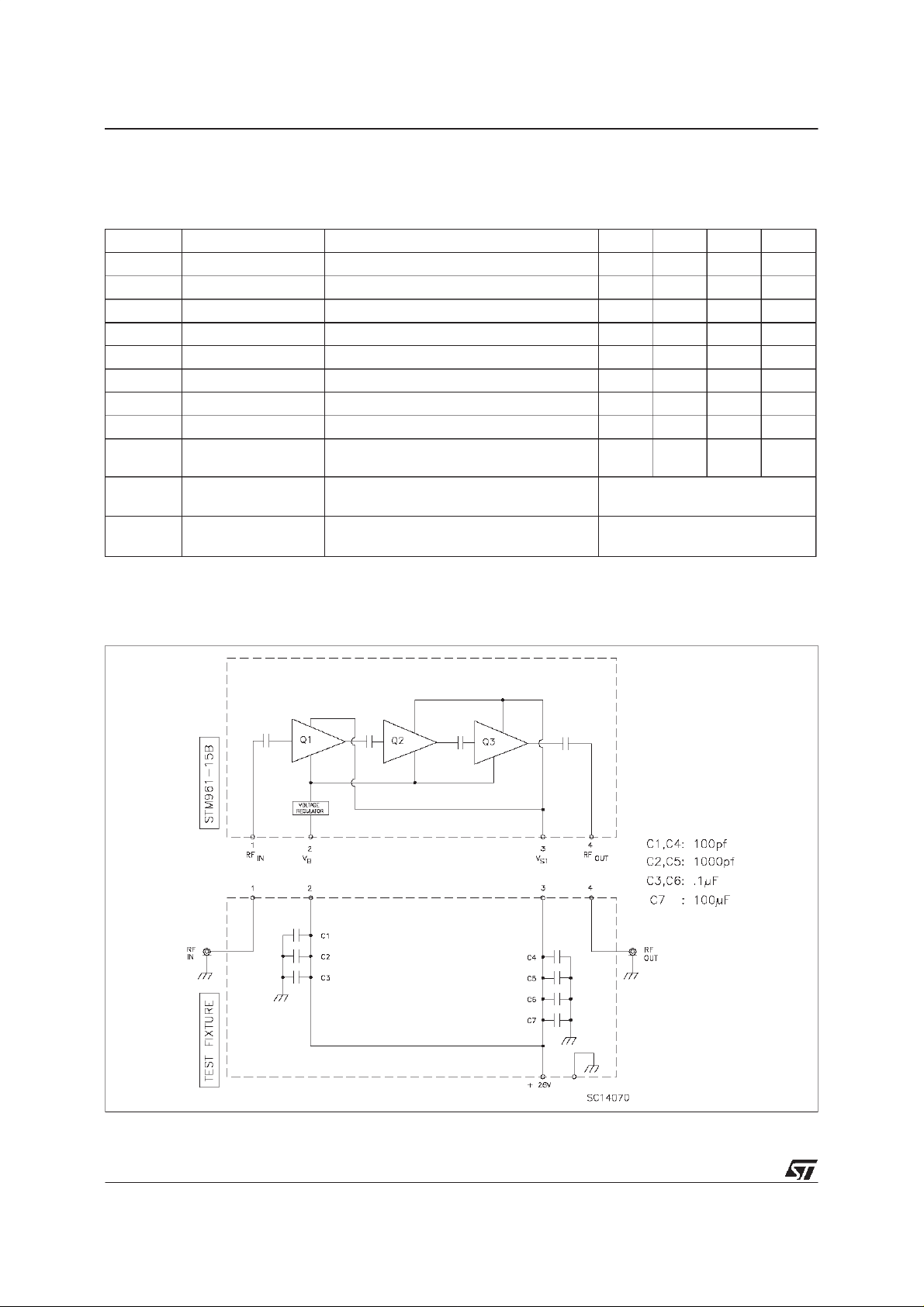
REF. 1017332I
MODULEDC AND TESTFIXTURE CONFIGURATION
2/7
REF. 1014532D
Page 3
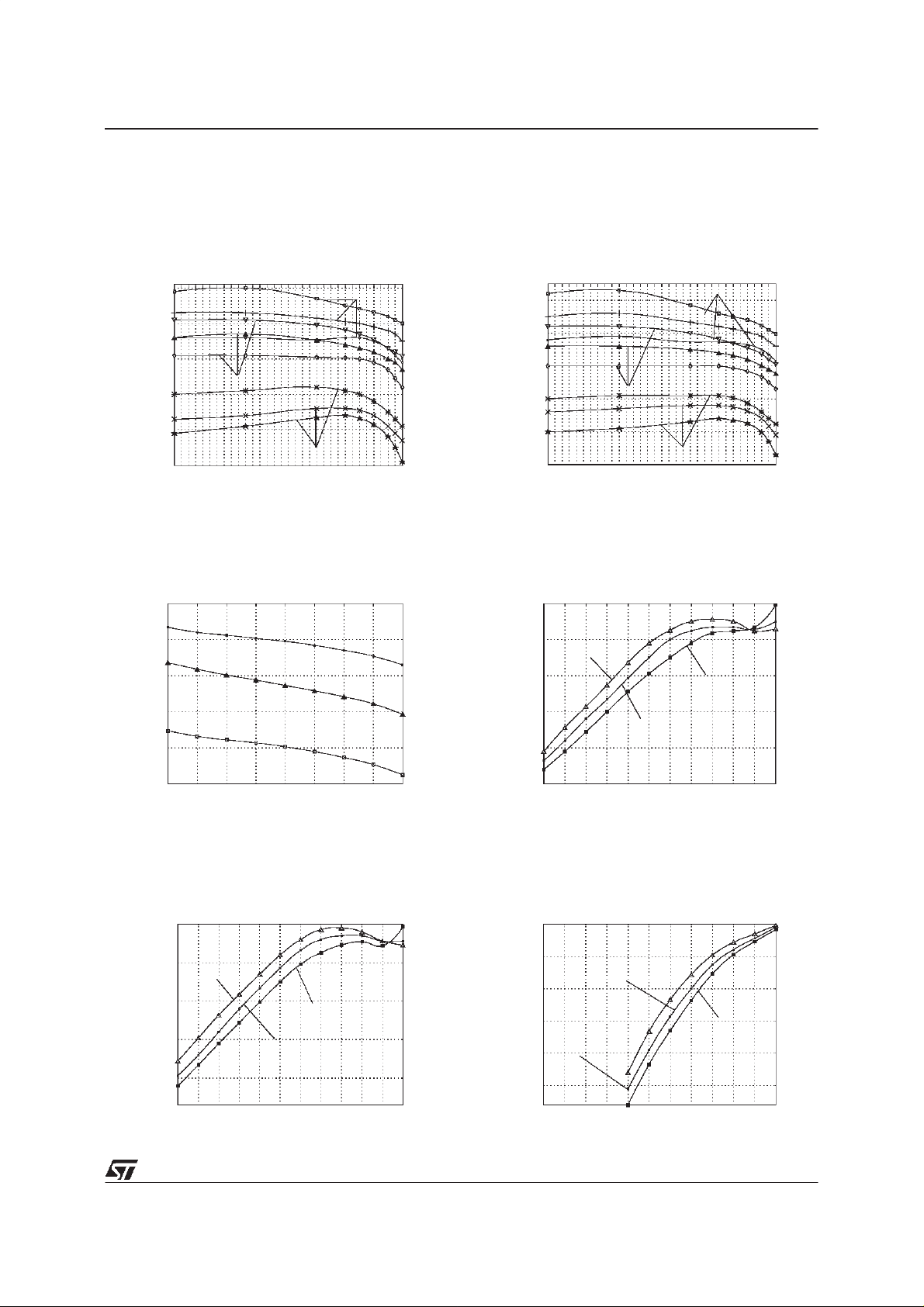
TYPICALPERFORMANCE
STM961-15B
PowerGainvs OutputPower
34
27.0 v
26.0 v
33
27.0 v
26.0 v
25.0 v
25.0 v
32
Tcase= +25 deg.C
27.0 v
31
POWER GAIN [dB]
26.0 v
25.0 v
30
f=960 MHz
29
10 20 30 34 36 38 40 42
Tcase= +85 deg.C
OUTPUT POWER [dBm]
Tcase= -10 deg.C
PowerGainvs Frequency& Temperature
34
33
32
Tc=-10 deg.C
Tc=+25 deg.C
PowerGain vs OutputPower
27.0 v
34.5
26.0 v
27.0 v
25.0 v
33.5
26.0 v
32.5
25.0 v
27.0 v
31.5
26.0 v
POWER GAIN [dB]
25.0 v
30.5
f=915 MHz
29.5
10 20 30 34 36 38 40 42
Tcase=+25 deg.C
OUTPUT POWER [dBm]
Tcase=-10 deg.C
Tcase=+85 deg.C
3rd Order IMD vs Output Power & Temperature
-25
-30
Tcase=-10 deg.C
-35
Tcase=+85 deg.C
31
POWER GAIN [dB]
30
Po=42 dBm CW
Vs=26.0 V
29
900 910 920 930 940 950 960 970 980
Tc=+85 deg.C
FREQUENCY [MHz]
3rd Order IMD vs OutputPower & Temperature
-26.5
-31.5
Tcase=-10 deg.C
-36.5
-41.5
3rd IMD [dBT]
-46.5
20 22 24 26 28 30 32 34 36 38 40 42
Tcase=+85 deg.C
Tcase=+25 deg.C
PEP [dBm]
Freq.=915 MHz
Vs=26.0 V
-40
3rd IMD [dBT]
-45
-50
20 22 24 26 28 30 32 34 36 38 40 42
Tcase=+25 deg.C
PEP [dBm]
Freq.=960 MHz
Vs=26.0 V
see note 1
5th Order IMD vs OutputPower & Temperature
-33
-38
-43
-48
3rd IMD [dBT]
-53
-58
20 22 24 26 28 30 32 34 36 38 40 42
see note 1see note 1
Tcase=-10 deg.C
Tcase=+25 deg.C
PEP [dBm]
Tcase=+85 deg.C
Freq.=960 MHz
Vs=26.0 V
3/7
Page 4

STM961-15B
TYPICALPERFORMANCE
5th Order IMD vs Output Power & Temperature
-33
-38
-43
-48
3rd IMD [dBT]
-53
-58
20 22 24 26 28 30 32 34 36 38 40 42
Tcase=-10 deg.C
Tcase=+25 deg.C
PEP [dBm]
Tcase=+85 deg.C
Freq.=915 MHz
Vs=26.0 V
Efficiencyvs Frequency
38.5
37.5
36.5
EFFICIENCY [%]
35.5
34.5
900 910 920 930 940 950 960 970 980
FREQUENCY [MHz]
Tcase=+25 deg.C
Po=42 dBm CW
Vs=25.0 V
Vs=26.0 V
Vs=27.0 V
see note 1
CW Efficiencyvs OutputPower& Temperature CW Efficiencyvs OutputPower& Temperature
37
32
27
Tcase=-10 deg.C
Tcase=+25 deg.C
37
32
27
Tcase=-10 deg.C
Tcase=+25 deg.C
22
17
CW EFFICIENCY [%]
12
7
32 34 36 38 40 42
OUTPUT POWER [dBm]
Tcase=+85 deg.C
Freq.=960 MHz
Vs=26.0 V
VSWRvs Frequency& Temperature
2
Vs=26.0 V
Po=42 dBm CW
1.8
Tcase=+85 deg.C
1.6
VSWR
1.4
1.2
1
900 910 920 930 940 950 960 970 980
Tcase=+25 deg.C
Tcase=-10 deg.C
FREQUENCY [MHz]
22
17
CW EFFICIENCY [%]
12
7
32 34 36 38 40 42
OUTPUT POWER [dBm]
Tcase=+85 deg.C
Freq.=915 MHz
Vs=26.0 V
Note (1) :
Two-tone test; 20KHz separation;
IMD (in dBT) is referencedto the individual tone level.
4/7
Page 5

STM961-15B
APPLICATIONS RECOMMENDATIONS
OPERATIONLIMITS
The STM961-15B power module should never
be operated under any condition which exceeds
the Absolute Maximum Ratings presented on
this data sheet. Nor should the module be
operated continuously at any of the specified
maximum ratings. If the module is to be
subjected to one or more of the maximumrating
conditions, care must be taken to monitor other
parameterswhich may be affected.
DECOUPLING
Failure to properly decouple any of the voltage
supply pins will result in oscillations at certain
operating frequencies. Therefore, it is
recommended that these pins be bypassed as
indicated in the Module DC and Test Fixture
Configurationdrawingof thisdatasheet.
MODULEMOUNTING
To insure adequate thermal transfer from the
module to the heatsink, it is recommended that
a satisfactory thermal compound such as Dow
Corning 340, Wakefield 120-2 or equivalent be
applied between the module flange and the
heatsink.
The heatsink mounting surface under the
module should be flat to within ± 0.05mm (±
0.002 inch). The module should be mounted to
the heatsink using 3.5 mm (or 6-32) or
equivalent screws torqued to 5-6 kg-cm (4-6
in-lb).
The module leads should be attached to
equipment PC board using 180°C solder
applied to the leads with a properly grounded
soldering iron tip, not to exceed 195°C, applied
a minimum of 2 mm (0.080 inch) from the body
of the module for a duration not to exceed 15
seconds per lead. It is imperative that no other
portion of the module, other than the leads, be
subjected to temperatures in excess of 100°C
(maximum storagetemperature), for any period
of time, as the plastic moulded cover, internal
components and sealing adhesives may be
adverselyaffected by suchconditions.
Due to the construction techniques and
materials used within the module, reflow
soldering of the flange heatsink or leads, is not
recommended.
THERMALCONSIDERATIONS
It will be necessary to provide a suitable
heatsink in order to maintain the module flange
temperature at or below to maximum case
operating temperature. In a case where the
module output power limited to +42 dBm CW
and designing for the worst case efficiency of
32%, the power dissipated by the module will
be 33.6 Watts. The heatsink must be designed
such that the thermal rise will be less than the
difference between the maximum operating
case temperature of the module while
dissipating33.6W.
At T
= +85oC, V = 26V, ZL=50Ωand P
case
OUT
= 42 dBm, maximum junction temperatures for
the individual transistors should be below the
followingvalues:
Q1 = 140
o
C, Q2 = 145oC, Q3 =130oC.
5/7
Page 6

STM961-15B
H110 MECHANICAL DATA
DIM.
MIN. TYP. MAX. MIN. TYP. MAX.
A 48.01 48.51 1.890 1.910
B 29.72 30.22 1.170 1.190
C 15.12 15.49 0.595 0.610
D 8.89 9.55 0.350 0.376
E 3.05 3.42 0.120 0.135
F 4.06 0.160
G 0.13 0.38 0.005 0.015
H 40.64 1.600
J 35.94 1.415
K 33.40 1.315
M 15.62 0.615
N 13.08 0.515
P 0.38 0.63 0.015 0.025
Q 3.81 4.06 0.150 0.160
R 17.40 19.55 0.685 0.770
S 8.77 9.77 0.345 0.385
T 4.52 5.72 0.178 0.225
mm inch
6/7
1014273H
Page 7

STM961-15B
Information furnished isbelieved tobe accurate and reliable. However, STMicroelectronics assumes no responsibility for the consequences
of use of such information nor for any infringement of patents or other rights of third parties which may result from its use. No license is
granted by implication or otherwise underany patent or patent rights of STMicroelectronics. Specification mentioned in this publication are
subject to change without notice. Thispublication supersedes and replaces allinformation previously supplied. STMicroelectronics products
are not authorized for use as critical components in life support devices or systems without express written approval of STMicroelectronics.
The ST logo is a trademark of STMicroelectronics
1999 STMicroelectronics – Printed in Italy – AllRights Reserved
STMicroelectronicsGROUP OF COMPANIES
Australia - Brazil -Canada - China -France -Germany - Italy - Japan - Korea - Malaysia -Malta -Mexico - Morocco - The Netherlands -
Singapore - Spain - Sweden -Switzerland - Taiwan - Thailand - United Kingdom - U.S.A.
http://www.st.com
.
7/7
 Loading...