

Page 1
■ LINEARPOWER AMPLIFIER
■ 890-915MHz
■ 12.5 VOLTS
■ INPUT/OUTPUT50 OHMS
■ POUT = 16 W MIN.
■ GAIN = 42 dB MIN.
DESCRIPTION
The STM915-16 is a linear power module
designed for 12.5 V applications in GSM Cellular
Radio Systems. The STM915-16 uses gold
metallized transistors with diffused emitter ballast
resistors for high linearity Class AB operation.
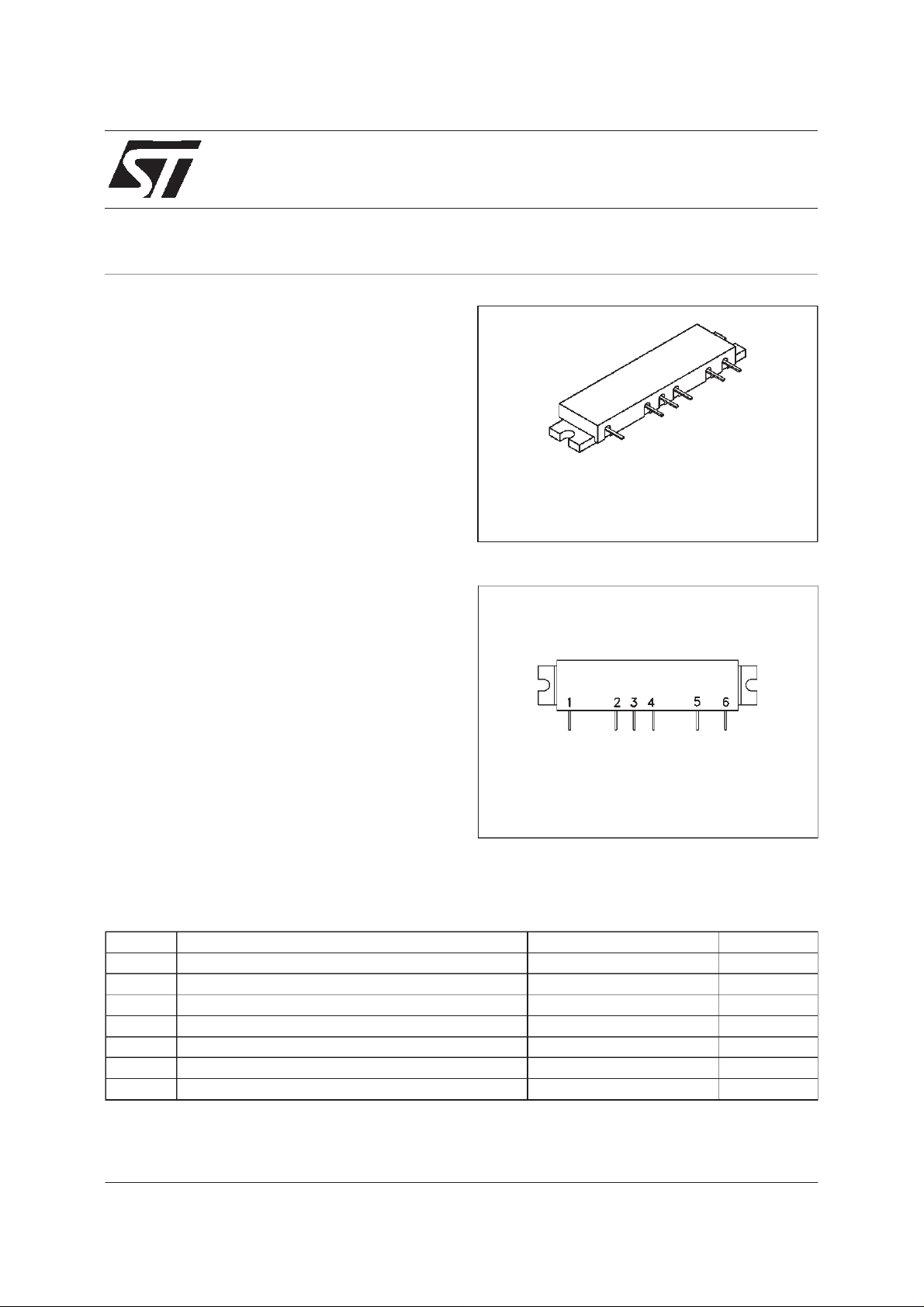
STM915-16
RF POWER MODULE
GSM MOBILE APPLICATIONS
CASE H100
ORDER CODE BRANDING
STM915-16 STM915-16
PIN CONNECTION
1 RF Input 4 8.0 Vdc
2 8.0Vdc 5 12.5 Vdc
3 12.5 Vdc 6 RF Output
ABSOLUTE MAXIMUM RATINGS (T
Symb o l Para meter Val u e Unit
V
S2,VS4
V
S1,VS3
V
CONTROL
P
P
OUT
T
T
Note1: Pulse Width= 577 µsec.
June 1999
DC Supply V olt ag e (RF appl ied / No RF ap plied ) 15.6/ 30.0 Vdc
DC Supply V olt ag e 8.5 Vdc
DC Contr o l Voltage 4.5 Vdc
RF I nput P ower (P
IN
1
RF O utpu t Power (VS2,VS4=12.5V) 20 W
Sto rage Tempe r ature - 30 to + 100
STG
Oper ating Case Tem peratu re - 30 to + 100
C
Repetition rate = 4.6 msec.
OUT
=25oC)
case
≤ 17 W)
3.0 mW
o
C
o
C
1/7
Page 2
STM915-16
ELECTRICALSPECIFICATIONS(T
case
25°C, V
=
S1
, V
S3
=
8.0 Vdc; V
S2
, V
S4
=
12.5 Vdc)
Symbol Parame ter Test Condi tio ns Value Unit
Min. Typ. Max.
BW Frequ e nc y Range 890 915 MHz
P
I
I
I
Output Power
OUT
η
Efficiency
Leakag e Curr en t ,
Q1
V
S1,VS2
Bias Curre nt,
Q2
V
S3
Quiescent Current ,
Q3
V
S4
Contr ol Dynamic
Range
Isol at i on
H Harmonics
VSWR
V
CONT
I
CONT
Input VS WR
IN
Contr ol Volt a ge 0 4.0 Vdc
Contr ol Current 1.0 2.0 mA
1,2
1, 2
3
1, 2
1,2
V
P
V
V
V
V
V
P
P
=
4.0 Vdc PIN= 1mW
CONT
16 W
=
OUT
=
0Vdc PIN=
CONT
=
0Vdc PIN=
CONT
=
0Vdc PIN=
CONT
=
0to4.0V
CONT
=
0Vdc V
CONT
=
42 dBm reference
OUT
=
+13dBmto+42dBm
OUT
S2, S4
1mW
1mW
1mW
=
0 to 15. 6V
16 W
35 41 %
0.5 2.0 mA
140 150 mA
200 250 mA
56 dB
−14 d Bm
−45 dBc
2.0:1
T
r
Notes: 1) P
2) PulseWidth
Repetition rate
Rise Time
Noise Power 30 KHz B and width, 20 MH z ab ove f
Stab ilit y
Load Mi s match
1.0mW adjust V
IN =
1, 2, 4
1, 2
CONTROL
577 µsec. 4)Trmeasured at 1% to81% ofP
=
4.6 msec.
=
P
=
+13 to +42 dBm
OUT
P
=
+13dBmto+42dBmCW
OUT
P
= − 14 to +42 dBm
OUT
=
V
S2,VS4
Load VSWR
10.8to15.6V
=
6:1 Sourc e VS WR= 3:1
All phase angles T
1,2
VSWR= 10:1 Al l p hase angles
=
15.6Vdc P
V
forspecified P
OUT
OUT
.3)P
=
− 20 to + 6 0°C
C
= 16 W
(Reference) =42 dBm
OUT
1.0 µSec
0
−70 −65 dBm
AllSpurious outputs more
than 60dB below carrier
No Degradationin Output
Power
OUT
in watts
REF. 1014655E
GSM SPECIFIC TESTS
Symbol Parameter Test Conditi ons Value Unit
Min. Typ. Max.
AM/AM Conversion
Gain
PIN= fo(0 dBm)+[fo+200kHz(−40 dBm )]
V
CONT RO L
P
OUT
P
OUT(fo
P
OUT(fo
adjusted for
= 13, 30, 42 dBm
+200kHz)
− 20 0 k Hz )
− 40
− 45
dBc
dBc
2/7
AM/PM Conversion
= +13 t o + 42 dBm
P
OUT
varied +/− .5 dB
P
IN
4 °/dB
Page 3

MODULEDCAND TEST FIXTURE CONFIGURATION
STM915-16
REF. 1015959E
3/7
Page 4

STM915-16
TYPICALPERFORMANCE
OutputPowervs Frequency
ControlVoltagevs Case Temperature
ControlVoltage,Efficiency & Input VSWR vs
Frequency
OutputPower vs Case Temperature
OutputPowervs ControlVoltage
4/7
Page 5

APPLICATIONS RECOMMENDATIONS
STM915-16
OPERATIONLIMITS
The STM915-16 power module should never be
operated under any condition which exceeds
the Absolute Maximum Ratings presented on
this data sheet. Nor should the module be
operated continuously at any of the specified
maximum ratings. If the module is to be
operated under any condition such that it may
be subjected to one or more of the maximum
rating conditions,care must be taken to monitor
other parameters which may be affected. For
example, a combination of high V
and input
S3
overdrive could result in exceeding the
maximum output power rating; in this condition,
the output power must be maintainedbelow the
maximum rating by use of the gain control pin.
GAIN CONTROL
The module output power should be limited to
20 watts (43 dBm). The module is designed to
be operated with V
and VS4set to 12.5 Vdc and input power
V
S2
and VS3set to 8.0 Vdc,
S1
set to 1.0 mW (0 dBm).Module gain is adjusted
by varyingV
CONTROL
.
DECOUPLING
The bypassing internal to the module is
sufficient for the frequencyrange 90-1300 MHz.
Care should be taken to insure proper
decoupling for each application as the module
is capable of a wide range of operating
characteristics including ”linear” operation, in
which an important design criteria is the use of
appropriate bypassing. For bypassing low
frequencies while maintaining the electrical
specifications contained in this data sheet, use
of the decouplingnetwork shown in the ”Module
DC and Test Fixture Configuration” diagram
herein is recommended.
The heatsink mounting surface under the module
should be flat to within ± 0.05 mm (± 0.002 inch).
The module should be mounted to the heatsink
using 3 mm (or 4-40) or equivalent screws
torquedto 5-6 kg-cm (4-6 in-lb).
The module leads are attached to the equipment
PC board using 180°Csolder applied to the leads
with it properly grounded soldering iron trip, not to
exceed 195°C, applied a minimum of 2 mm
(0.080 inch) from the body of the module for a
duration not to exceed 15 seconds per lead. It is
imperative that no other portion of the module,
other than the leads, be subjected to
temperatures in excess of 100°C (maximum
storage temperature), for any period of time, as
the plastic moulded cover, internal components
and sealing adhesivesmay be adverselyaffected
by such conditions.
Due to the construction techniques and the
materials used within the module, reflow
soldering of the flange heatsink or leads, is not
recommended.
THERMALCONSIDERATIONS
It will be necessaryto providea suitable heatsink
in order to maintain the module flange
temperature at or below the maximum case
operating temperature. In a case where the
module output power will be limited to +42 dBm
(16 W) and designing for the worst case
efficiency of 35%, the power dissipated by the
module will be 29.7 watts. The heatsink must be
designed such that the thermal rise will be less
than the difference between the maximum
ambient temperature at which the module will
operate and the maximum operating case
temperature of the module while dissipating 29.7
watts.
MODULEMOUNTING
To insure adequate thermal transfer from the
module to the heatsink, it is recommendedthat
a satisfactory thermal compound such as Dow
Corning 340, Wakefield 120-2 or equivalent be
applied between the module flange and the
heatsink.
5/7
Page 6

STM915-16
H100 MECHANICAL DATA
DIM.
A 60.45 60.83 2.380 2.395
B 50.04 50.54 1.970 1.990
C 11.31 11.81 0.445 0.465
D 6.35 6.73 0.250 0.265
E 2.16 2.54 0.085 0.100
F 3.35 0.132
G 0.13 0.38 0.005 0.015
H 57.40 2.260
J 51.87 2.042
K 39.17 1.542
L 34.09 1.342
M 29.01 1.142
N 16.31 0.642
P 8.69 0.342
Q 0.38 0.64 0.015 0.025
R 3.05 3.30 0.120 0.130
S 13.59 14.09 0.535 0.555
V 4.49 5.51 0.177 0.217
W 6.78 7.06 0.267 0.278
MIN. TYP. MAX. MIN. TYP. MAX.
mm inch
6/7
1013762F
Page 7

STM915-16
Information furnished isbelieved tobe accurate and reliable. However, STMicroelectronics assumes no responsibility for the consequences
of use of such information nor for any infringement of patents or other rights of third parties which may result from its use. No license is
granted by implication or otherwise under any patent or patent rights of STMicroelectronics. Specification mentioned in this publication are
subject to change without notice. Thispublication supersedes and replaces all information previously supplied. STMicroelectronics products
are not authorized for use as critical components in life support devices or systems without express written approval of STMicroelectronics.
The ST logo is a trademark of STMicroelectronics
1999 STMicroelectronics – PrintedinItaly– All Rights Reserved
STMicroelectronicsGROUP OF COMPANIES
Australia - Brazil -Canada - China - France -Germany - Italy- Japan - Korea - Malaysia - Malta - Mexico - Morocco - The Netherlands-
Singapore - Spain - Sweden -Switzerland- Taiwan -Thailand - United Kingdom - U.S.A.
http://www.st.com
.
7/7
 Loading...