

Page 1
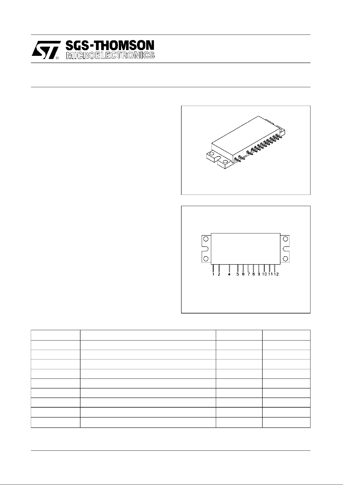
CASE STYLEH 14 1
RF POW ER MO DU LE
LINEAR BASE STATI ON APPLIC ATIONS
.LINEAR POWER AMPLIFI ER
.860 - 900 MHz
.26 VOLTS
.INPUT/OUTPUT 50 OHMS
.P
OUT
= +44.7 dBm PEP
.GAIN
=
35 dB MIN.
DESCRI P TI ON
The STM901-30 module is d esigned for d igital
cellular radio ba se station a pplications in t he
860-900 MHz fr equency range operating at
26V.
The STM901-30 is designed t o meet the low
distortion, high linearity requirements of modern digital cellular base station e quipment.
PI N CONNE CTION
ABSOLUTE MAXIMUM RATINGS (Tcase = 25°C)
STM 9 01- 30
1. RF Input 2. V
G1
3. deleted 4. V
G2
5. V
D
6. V
B1
7. Cap18. V
C1
9. V
B2
10. Cap211. V
C2
12. RF Output
ORDERCODE
STM901-30
BRANDING
STM901-30
Symbol Parameter Value Unit
V, VD,VC1,VC2DC Supply Voltage 28 Vdc
I
Q1 Bias Current @ V
= 26V, 1st Stage
0.40 Adc
I
Q2 Bias Current @ V = 26V, 2nd St age
0.40 Adc
I
Q3 Bias Current @ V = 26V, 3rd St age
0.54 Adc
I
Q4 Bias Current @ V = 26V, 4th Stage
1.62 Adc
P
IN
RF Input Power (P
OUT
< 4 4.7 dBm PEP) 14 dBm PEP
P
OUT
RF Ou t p ut Powe r (V = 26V)
48 dBm PEP
T
STG
Storage Temperature
− 30 to +100
°
C
T
OPER
Operating Temperature
− 30 to +100
°
C
October 31, 1997 1/8
Page 2
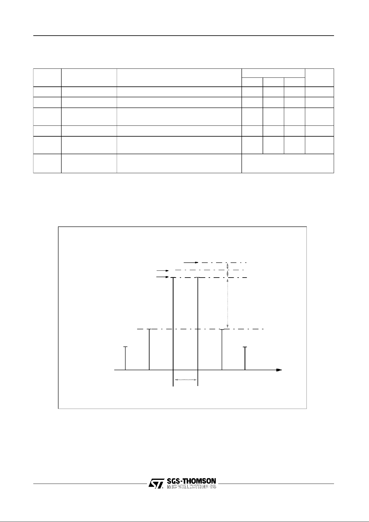
ELECTRICAL SP ECI FICATIONS (T
case
=25°C, VD,VC1,VC2= 26V) (I
DQ1
= 100 mA,
I
DQ2
= 180mA, I
CQ1
=50mA,I
CQ2
=150mA)
Symbol Parameter Test Cond itions
Value
Uni t
Min. Typ. Max.
BW Frequency Range 860 — 900 MHz
G
P
Power Gain
P
OUT
=
+44.7 dBm PEP
35 38 — dB
η
dt
*
Double-Tone
Efficiency
P
OUT
=
+44.7 dBm PEP
27 30 — %
Input VSWR
P
OUT
=
+44.7 dBm PEP
— 1.5:1 3:1
IMD* Intermodulation
Distortion
P
OUT
=
+44.7 dBm PEP
—
−33 −26
dBT**
— Load Mismatch
VSWR
=
5:1 V= 26Vdc
P
OUT
=
+44.7 dBm PEP
No Degradation in Output
Power
Note : * Tw o-Tone test ; 20 KHz sep ar ation ** dB T - i n dB, referenced t o tone lev el (See Fi gur e 1 belo w )
20 kHz
PEP (PeakEnvelope Power)Carrier Level
Total Avg. Powerof TwoTone
AVERAGE Powerof Each Tone
3 dB min
3 dB min
26 dB min
freq
Max IMD in dBT
Figure 1
STM901-30
2/8 October 31, 1997
Page 3
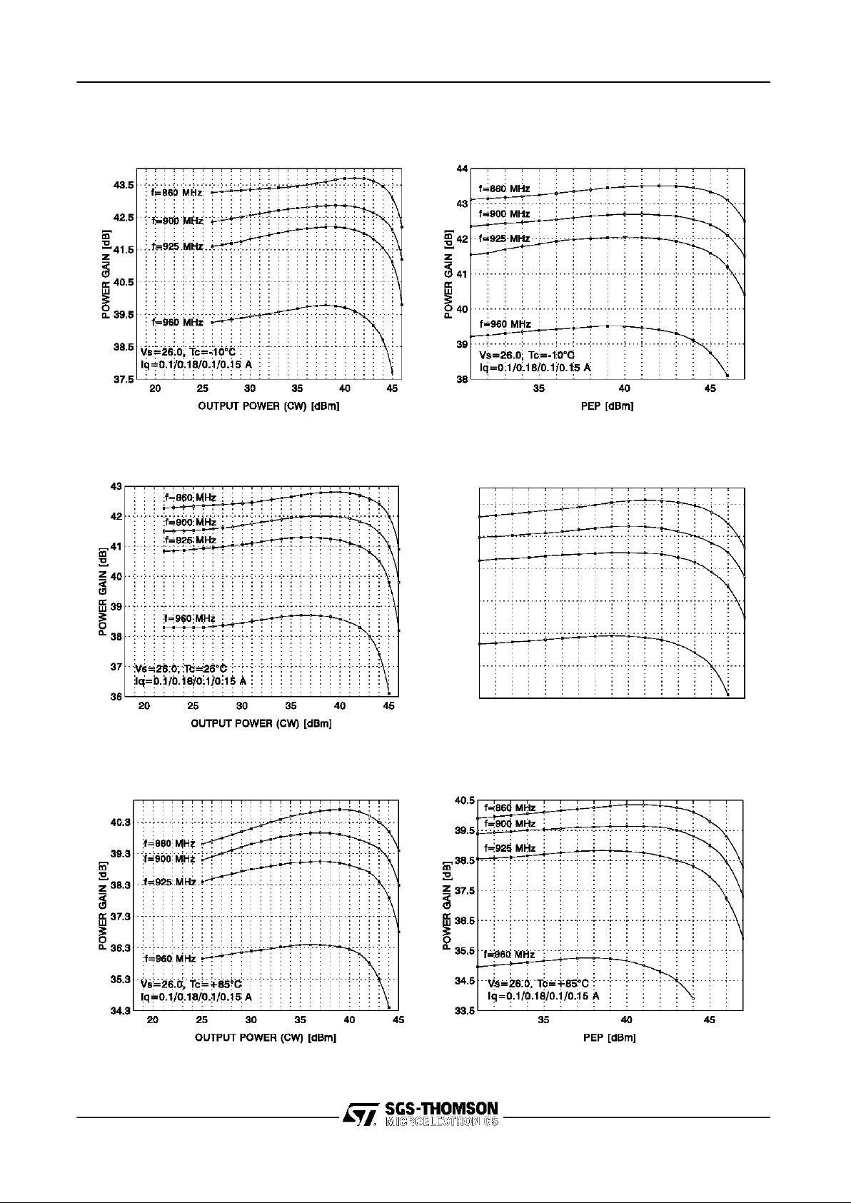
POWER GAIN vs OUTPUT POWER &
FREQUENCY
POWER GAIN vs OUTPUT POWER &
FREQUENCY
POWER GAIN vs OUTPUT POWER &
FREQUENCY
POWER GAIN vs PEP & FREQUENCY
POWER GAIN vs PEP & FREQUENCY
POWER GAIN vs PEP & FREQUENCY
PEP [dBm]
POWER GAIN [dB]
35 40 45
36.5
37.5
38.5
39.5
40.5
41.5
42.5
f=900 MHz
f=860 MHz
f=925 MHz
f=960 MHz
Vs=26.0, Tc=25°C
Iq=0.1/0.18/0.1/0.15 A
TYPICAL PERFORMANCE
STM901-30
October 31, 1997 3/8
Page 4

5th ORDER IMD vs PEP
5th ORDER IMD vs PEP
5th ORDER IMD vs PEP
3rd ORDER IMD vs PEP
3rd ORDER IMD vs PEP
3rd ORDER IMD vs PEP
PEP [dBm]
3rd IMD [dBT]
20 25 30 35 40 45
-20
-25
-30
-35
-40
f=900 MHz
f=860 MHz
f=925 MHz
f=960 MHz
Vs= 26.0, Tc=+85°C
Iq=0.1/0. 18/0. 05/0.15 A
TYPICAL PERFORMANCE
STM901-30
4/8 October 31, 1997
Page 5

GAIN & RETURN LOSS vs FREQUENCY
EFFICIENCY vs FREQUENCY
CW EFFICIENCY vs OUTPUT POWER
& FREQUENCY
TYPICAL PERFORMANCE
STM901-30
October 31, 1997 5/8
Page 6

C1, C3, C 5, C7, C11, C 13, C 17 : 100 pF
C2, C4, C 6, C8, C12, C 14, C 18 : . 001 µF
C19 : .1µF
C20, C22 : 100 µF
F1, F 2, F3 : FAIR-RITE #2664000101
L1, L2, L3 : 5 T ur ns of 24 AWG Wir e, Inner Dia met er
1.27mm
R1, R2, R3, R4 : 20 KOHM
Setting Bias: (Ex.: I
Q1
=
.1A, I
Q2
=
.18A, I
Q3
=
.050A, I
Q4
=
.150A)
1. Set all variable resistors clockwise. (No bias current flows through
transistors when all variable resistors are set clockwise.)
2. Record stationary current IO.
3. Adjust R1 for (IO+ 100)mA.
4. Adjust R2 for (IO+ 100 + 180)mA.
5. Adjust R3 for (IO+ 100 + 180 + 50)mA.
6. Adjust R4 for (IO+ 100 + 180 + 50 + 150)mA.
MODULE DC AND TES T FIXTURE CONFI G URATION
STM901-30
6/8 October 31, 1997
Page 7

APPLI CATI O NS RECOMMENDATI ONS
OPERATION LIMITS
The STM901-30 power module should never be operated under any condition which exceeds the Absolute Maximum Ratings presented on this data
sheet. Nor should the module be operated continuously at any of the specified maximum ratings. If
the module is to be operated under any condition
such that it may be subjected to one or more of the
maximum rating conditions, care must be taken to
monitor other parameters which may be affected.
DECOUPLING
Failure to properly decouple any of the voltage supply pins will result in oscillations at certain operating
frequencies. Therefore, it is recommended that
these pins be bypassed as indicated in the Module
DC and Test Fixture Configuration drawing of this
data sheet.
MODULE MOUNTING
To insure adequate thermal transfer from the module to the heatsink, it is recommended that a satisfactory thermal compound such as Dow Corning
340, Wakefield 120-2 or equivalent be applied between the module flange and the heatsink.
The heatsink mounting surface under the module
should be flat to within +/- 0.05 mm (+/- 0.002
inch). The module should be mounted to the
heatsink using 3 mm (or 4-40) or equivalent screws
torqued to 5-6 kg-cm (4-6 in-lb).
The module leads are attached to the equipment
PC board using 180°C solder applied to the leads
with a properly grounded soldering iron tip, not to
exceed 195°C, applied a minimum of 2 mm (0.080
inch) from the body of the module for a duration not
to exceed 15 seconds per lead. It is imperative that
no other portion of the module, other than the
leads, be subjected to temperatures in excess of
100°C (maximum storage temperature), for any period of time, as the plastic moulded cover, internal
components and sealing adhesives may be adversely affectedby such conditions.
Due to the construction techniques and the materials used within the module, reflow soldering of the
flange heatsink or the leads, is not recommended.
THERMAL CONSIDERATIONS
It will be necessary to provide a suitable heatsink in
order to maintain the module flange temperature at
or below the maximum case operating temperature.
In a case where the module output power will be
limited to +44.7 dBm (30W PEP) and designing for
the worst case double-tone efficiency of 25%, the
power dissipated by the module will be 48 watts.
The heatsink must be designed such that the thermal rise will be less than the difference between
the maximum ambient temperature at which the
module will operate and the maximum operating
case temperature of the module while dissipating
48 watts.
At T
case
= +85°C, V = 26v, IQ1= 0.1A, IQ2= 0.18A,
I
Q3
= 0.05A, IQ4= 0.2A, ZL= 50 ohms and P
OUT
=
+44.7dBm PEP, maximum junction temperatures for
the individual transistors should be below the following values:
Q1 = 115°C
Q2 = 130°C
Q3 = 125°C
Q4 = 145°C
STM901-30
October 31, 1997 7/8
Page 8

PACKAGE MECHANICAL DATA
UDCS No. 1010946 rev D
Inform ation furnished is believed to be accurat e a nd rel iable. However, SGS-T H O MS O N Microelectroni cs assumes no responsibility for
the consequences of use of such inf or mat ion nor for any infri ngement of patent s or ot her ri ght s of thir d par t i es which ma y result from
its use. N o license is granted by i mplicati on or otherw i se under any patent or patent ri ghts of SG S - T H O M S O N Mi c roe le ctronics.
Specificati ons ment ioned in t hi s publ ication ar e subject t o c hange with out not ice. This publi cat ion supers edes and replaces all
infor m at i on previously suppl ied. SGS- THOM S O N Microelectronics products are not authorized f or use as critical components in li fe
support device s or syst ems wit hout express writ t e n approval of S G S - THOMSO N Microelectr oni c s.
1997 SGS-THOMSON Microelectroni cs - All Rights Reserved
SGS-THOMSON Microelectronics GROUP O F COMPANIES
Austr alia - Brazil - Canada - China - France - Germany - Ita ly - Japan - Korea
Mal ays i a - Malt a - Morocco - The Net herlands - Singapor e - Spain - Sweden - Swit zerland
Taiwan - Thail and - U ni ted K i ngdom - U.S.A.
RF Pr oduc t s Divi s i on
141 Commerce Drive Montgomeryville, PA 18936
tel 215-361-6400 fax 215-36 2-12 93
STM901-30
8/8 October 31, 1997
 Loading...