

Page 1
STM7E1A
7 E 1 CHANNELS SWITCH ARRAY
■ MAIN SWITCHES MAX. R
■ PROVIDES 7 AUXILIARY SWITCHES WITH
R
<75Ω
ON
■ 6V
AMPLITUDE OF ANALOG INPUT
PP
LESS THAN 2Ω
ON
SIGNAL
■ DIGITAL INPUTS ARETTL LEVELS
COMPATIBLE
DESCRIPTION
The STM7E1 consists in 7 identical ISDN E1
channels, each channel corresponding to 4 main
low-resistant switches (a and b) and 2 auxiliary
switches (c and d). The switches posi tion s in all
the channels are identical and c ontrolled by a
unique control resource driven by the digital inputs
Lm, Ls and Sc.
In each c hannel, t he TX and RX lines can be
switched bet ween a Main port or a Spare-port by
the main switches: if both "a" switches are closed
and both "b" switches are open, the Main port is
connected to the line, while if both "a" switches
are open and both "b' switches are clo se d, the
spare port is connected to the line.
The 2 auxiliary switches enable to close a local
loop between the TX and RX a ccess of a port: if
"c" is closed, the Spare port RX and TX access is
connected between each other to fo rm a local
loop, while if "d" is closed, the Main port RX and
TX access is connected between each other to
form a local loop.
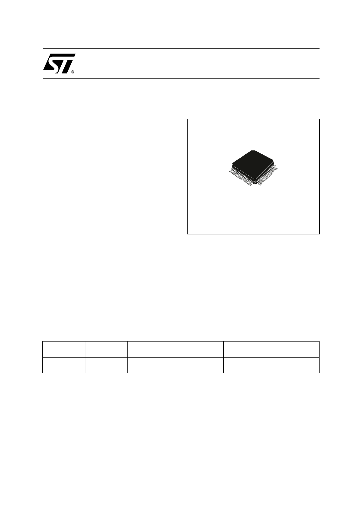
TQFP64
The Spare port is only used for test purpose on the
system board while the Main port is the
communication channel. Consequently, a
switching from the Main port to the Spare port
occurs very rarely (<10 times a day).
The power sup plies of the chip need to be de
coupled properly. This means that at least one
external capacitor C1 must be connected in
between GND and VPOS, one external c apac it or
C2 between GND and VNE G, and one external
capacitor C3 between each pair of VNEG and
VPOS.
ORDERING CODES
Type
STM7E1A -40 to 85 °C TQFP64 (Tray) 160 parts per Tray
STM7E1AR -40 to 85 °C TQFP64 (Tape & Reel) 1000 parts per reel
Temperature
Range
Package Comments
1/10December 2002
Page 2
STM7E1A
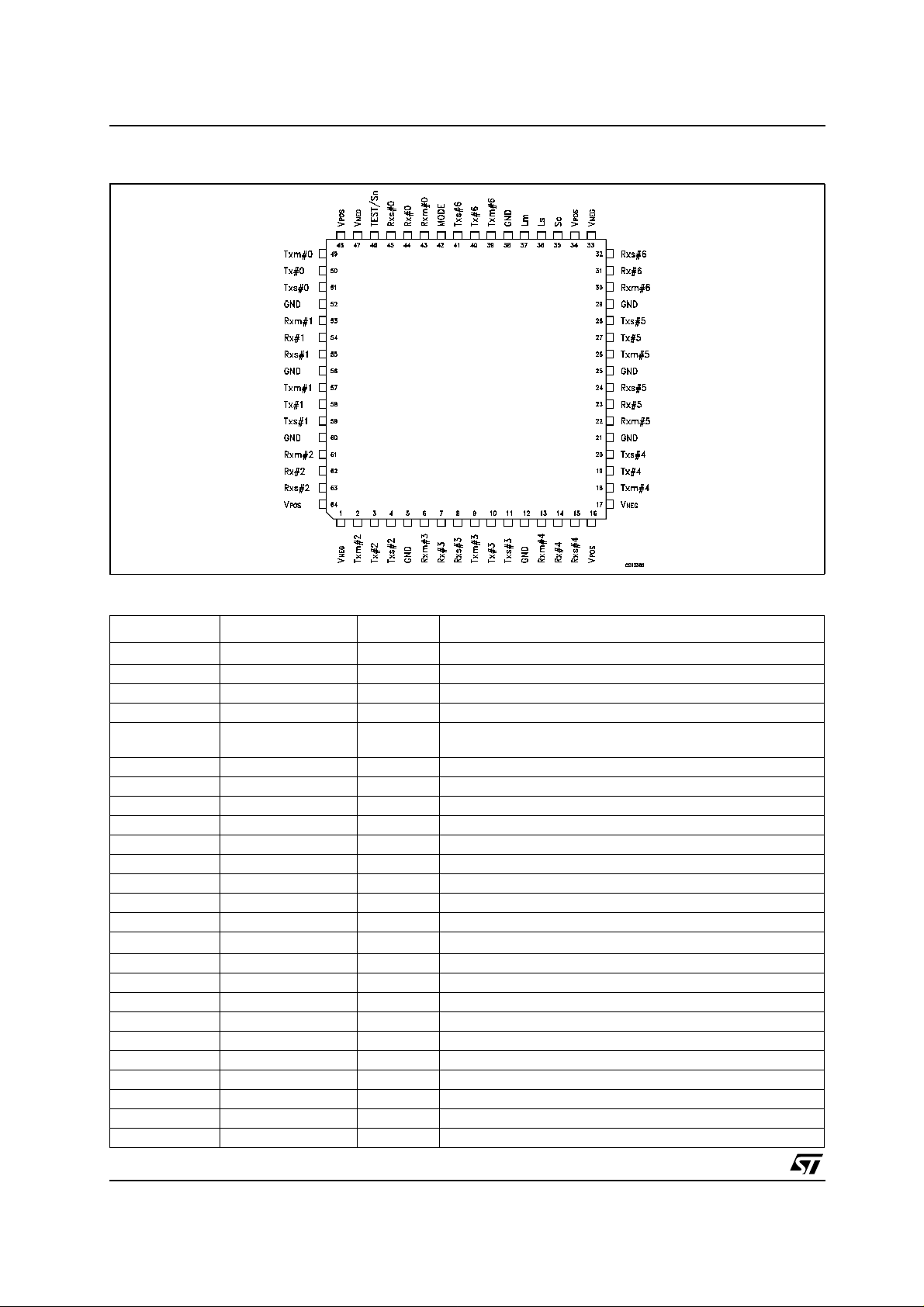
PIN CONFIGURATION
PIN DESCRIPTION
PlN N° SYMBOL TYPE NAME AND FUNCTION
1, 17, 33, 47 V
2 Txm#2 IOA Channel 2: TX main port
3 Tx#2 IOA Channel 2: TX line
4 Txs#2 IOA Channel 2: TX spare port
5, 12, 21, 25, 29,
38, 52, 56, 60
6 Rxm#3 IOA Channel 3: RX main port
7 Rx#3 IOA Channel 3: RX line
8 Rxs#3 IOA Channel 3: RX spare port
9 Txm#3 IOA Channel 3: TX main port
10 Tx#3 IOA Channel 3: TX line
11 Txs#3 IOA Channel 3: TX spare port
13 Rxm#4 IOA Channel 4: RX main port
14 Rx#4 IOA Channel 4: RX line
15 Rxs#4 IOA Channel 4: RX spare port
16, 34, 48, 64
18 Txm#4 IOA Channel 4: TX main port
19 Tx#4 IOA Channel 4: TX line
20 Txs#4 IOA Channel 4: TX spare port
22 Rxm#5 IOA Channel 5: RX main port
23 Rx#5 IOA Channel 5: RX line
24 Rxs#5 IOA Channel 5: RX spare port
26 Txm#5 IOA Channel 5: TX main port
27 Tx#5 IOA Channel 5: TX line
28 Txs#5 IOA Channel 5: TX spare port
30 Rxm#6 IOA Channel 6: RX main port
(1)
NEG
GND G
V
(2)
POS
P
P
Negative Power Supply
Voltage Reference for digital inputs
Positive Power Supply
2/10
Page 3
PlN N° SYMBOL TYPE NAME AND FUNCTION
31 Rx#6 IOA Channel 6: RX line
32 Rxs#6 IOA Channel 6: RX spare port
35 Sc I Control digital input
36 Ls I Control digital input
37 Lm I Control digital input
39 Txm#6 IOA Channel 6: TX main port
40 Tx#6 IOA Channel 6: TX line
41 Txs#6 IOA Channel 6: TX spare port
42 Mode I Control Digital Input
43 Rxm#0 IOA Channel 0: RX main port
44 Rx#0 IOA Channel 0: RX line
45 Rxs#0 IOA Channel 0: RX spare port
46 TEST/Sn I Channel 6: RX main port
49 Txm#0 IOA Channel 0: TX main port
50 Tx#0 IOA Channel 0: TX line
51 Txs#0 IOA Channel 0: TX spare port
53 Rxm#1 IOA Channel 1: RX main port
54 Rx#1 IOA Channel 1: RX line
55 Rxs#1 IOA Channel 1: RX spare port
57 Txm#1 IOA Channel 1: TX main port
58 Tx#1 IOA Channel 1: TX line
59 Txs#1 IOA Channel 1: TX spare port
61 Rxm#2 IOA Channel 2: RX main port
62 Rx#2 IOA Channel 2: RX line
63 Rxs#2 IOA Channel 2: RX spare port
NOTE 1: All VNEG pins to be connected together on board.
NOTE 2: All VPOS pins to be connected together on board.
STM7E1A
3/10
Page 4

STM7E1A
TYPICAL OPERATING CIRCUIT
Tx#0
Rx#0
LmLsScMODE TEST/Sn
Control Decoding
Level Shifting & Buffering
CHANNEL 0
a
b
cd
a
b
Txm#0
Txs#0
Rxm#0
Rxs#0
Tx#1
Rx#1
Tx#6
Rx#6
CHANNEL 1
CHANNEL 6
VNEG GND
Txm#1
Txs#1
Rxm#1
Rxs#1
Txm#6
Txs#6
Rxm#6
Rxs#6
VPOS
4/10
Page 5

STM7E1A
DECODING OF FUNCTIONAL M ODE 1 (MODE = L)
Main Switches Sc low a closed, b open Main port is connected to the line
Sc high a open, b closed Spare port is connected to the line
Auxiliary
Switches
When closing the main port local loop (Lm high), it is externalsystemresponsibilityto ensurethatthe main
port has previously been disconnected from the line (Sc has to be high). There is no internal mechanism
to ensure this.
When closing the spare port local loop (Ls high), it is external system responsibility to ensure that the
spare port has previously been disconnected from the line (Sc has to be high). There is no internal
mechanism to ensure this.
DECODING OF FUNCTIONAL M ODE 2 (MODE = H)
C = Closed
O=Open
Lm low d open Main port local loop open
Lm high d closed Main port local loop closed
Ls low c open Spare port local loop open
Ls high c closed Spare port local loop closed
INPUT OUTPUTS
TEST/Sn A_TX B_TX
LOC
HCO
INPUTS OUTPUTS
Sc Lm Ls A_RX B_RX c d
LLLCCOO
LLHCOCO
LHLOCOC
LHHCOOO
HL LOCOO
C = Closed
O=Open
TEST MODE DESCRIPTION (M ODE = 0, TEST = 1)
In order to test the main switches (4-point measurement), test modes are foreseen where the main
switches can be controlled independently from each other. One can en ter in test mode by controlling the
Sc, Lm and Ls pins according to the f ollowing table.
The digital part and auxiliary switches can be tested in functional mode.
Signification Sc Lm Ls
A_TX closed H H L
A_RX closed L H L
B_TX closed H L H
B_RX closed L L H
B_TX & c closed H L L
A_RX & d closed L L L
All main switches open
Note 1: Although there isaninternal pull down in the TEST pin, an external hardware connection from TEST to GND isrequired onthe board
to work in functional, mode.
HHH
LHH
5/10
Page 6

STM7E1A
ABSOLUTE M AX IMUM RATINGS
Symbol Description Min Max Unit
V
GND
V
Absolute Maximum Ratings are those values beyond which damage to the device may occur. Functional operation under these condition is
not implied.
RECOMMENDED OPERATING CONDITIONS
Symbol Parameter Min TYP Max Unit
V
POS
V
NEG
T
amb
T
I
peak,
switch
C
Positive Power Supply Voltage V
POS
Reference Ground V
Input Voltage for Digital Inputs and Analog Input/Output
IN
Pins
Positive Power Supply Voltage
Negative Power Supply Voltage
Ambient Temperature
Junction Temperature
J
Admissible peak Current in 1 Switch
Load Capacitance on ASIC output
Ia
- 0.3 V
NEG
- 0.3 V
NEG
- 0.3 V
V
NEG
NEG
NEG
NEG
+7
+7
+7
3.3 - 5% 3.3 + 5% V
-3.3 - 5% -3.3 + 5% V
-25 85 °C
-25 120 °C
300 mA
70 pF
V
V
V
DIGITAL PART SPECIFICATIONS
Symbol Parameter
Low Input Level 0 0.8 V
IL
High Input Level 2 V
IH
Low-High Switching Threshold Voltage 1.6 V
IT
Input Leakage Current -3 3
V
I
V
V
leak
Value
Min. Typ. Max.
POS
Unit
V
6/10
Page 7

STM7E1A
ANALOG PART SPECIFICATIONS
Symbol Parameter Test Condition
Min. Typ. Max.
(1)
R
ON(main)
R
ON(aux)
∆R
ON(main)
∆R
ON(main)
(1,2)
Roff
(3)
C
pin
A
peak,signal
(1,4)
f
signal
Cross-talk
On-resistance of the main
switches
(1)
On-resistance of the
auxiliary switches
(1)
Difference of RONbetween
VIN=2V,TA= 25°C 0.5 Ω
devices
(1)
Difference of RONbetween
VIN=2V,TA= 25°C 0.8 Ω
switches of the same device
Off-resistance of the main
100 kΩ
and auxiliary switches
Capacitance at any switch
pin, switch ON
(1)
Peak amplitude of the signal
-3 3 V
at switch pins
Frequency of the signal at
50 12000 KHz
switch pins (3dB bandwidth)
(1,5)
Cross-talk between lines 4 8 mV
t Switch time of the main
switches (a and b)
NOTE 1: all the parameters are valid only with a 75 Ω (±5%) load to GND.
NOTE 2: measured with a 5V DC voltage applied to a closed switch.
NOTE 3: not tested in production.
NOTE 4: measured with a 2Vpp signal.
NOTE 5: measured with the line connected to GND at one side with a 75
signal.
NOTE 6: during the switching between the main and spare ports, the behaviour of the component is not guaranteed: both main switches can
be open (break before make).
NOTE 7: measured with the line switching from a 2.5V DC level (main or spare port) to a -2.5V DC level (spare or main port).
Ω resistorand all the otherlinesdrivenby a1MHz,2Vppsinewave
Value
Unit
1.6 2 Ω
50 75 Ω
50 120 pF
p
rms
0.15 1 µs
CURRENT CONSUMPTION SPECIFICATIONS
Symbol Parameter
(1)
P
main
(1)
P
aux
I
STDBY(VNEG)
I
STDBY(VPOS)
E
SWITCH(VNEG)
E
SWITCH(VPOS)
NOTE 1: these parameters are not tested in production.
NOTE 2: this power is not delivered by V
NOTE 3: only valid with digital inputs to GND or V
Maximal average power dissipation in the main
switches
Maximal average power dissipation in the auxiliar
switches
(1,3)
Standby (no switching) current of VNEG -500 500 µA
(1,3)
Standby (no switching) current of VPOS -500 500 µA
(1)
Energy to be delivered to by VPOS when switching -100 100 nJ
(1)
Energy to be delivered to by VPOS when switching -100 100 nJ
POS
and V
supplies but by the signal sources.
NEG
levels.
POS
Value
Unit
Min. T yp. Max.
40 mW
150 mW
7/10
Page 8

STM7E1A
TQFP64 MECHANICAL DATA
DIM.
mm. inch
MIN. TYP MAX. MIN. TYP. MAX.
A 1.6 0.063
A1 0.05 0.15 0.002 0.006
A2 1.35 1.40 1.45 0.053 0.055 0.057
B 0.17 0.22 0.27 0.007 0.009 0.011
C 0.09 0.20 0.004 0.008
D 11.80 12.00 12.20 0.465 0.472 0.480
D1 9.80 10.00 10.20 0.386 0.394 0.402
D3 7.50 0.295
E 11.80 12.00 12.20 0.465 0.472 0.480
E1 9.80 10.00 10.20 0.386 0.394 0.402
E3 7.50 0.295
e 0.50 0.020
L 0.45 0.60 0.75 0.018 0.024 0.030
L1 1.00 0.039
K 0˚3.5˚7˚ 0˚3.5˚7˚
8/10
D
D1
D3
48
49
64
1
e
33
32
Seating Plane
E
E1
E3
L1
17
16
L
K
A1
0.10mm
.004
B
A
A2
C
0051434/E
Page 9

STM7E1A
Tape & Reel TQFP64 MECHANICAL DATA
mm. inch
DIM.
MIN. TYP MAX. MIN. TYP. MAX.
A 330 12.992
C 12.8 13.2 0.504 0.519
D 20.2 0.795
N 60 2.362
T 30.4 1.196
Ao 12.25 12.45 0482 0.490
Bo 12.25 12.45 0482 0.490
Ko 2.1 2.3 0.083 0.091
Po 3.9 4.1 0.153 0.161
P 15.9 16.1 0.626 0.639
9/10
Page 10

STM7E1A
Information furnished is believed to be accurate and reliable. However, STMicroelectronics assumes no responsibilit y for t he
consequences of use of such informatio n nor for any infringement of paten ts or o ther rig hts of t hird part ies which ma y result from
its use. No license is granted by implication or otherwise under any patent or patent rights of STMicroelectronics. Specifications
mentioned in this publication are subject to change without notice. This publication supersedes and replaces all information
previousl y suppl ied. STM icroel ectronics produc ts are not auth orized for use as c ritica l compone nts in l ife s upport dev ices or
systems without express written approval of STMicroelectronics.
Australia - Brazil - Canada - China - Finland - France - Germany - Hong Kong - India - Israel - Italy - Japan - Malaysia - Malta - Morocco
© The ST logo is a registered trademark of STMicroelectronics
© 2002 STMicroelectronics - Printed in Italy - All Rights Reserved
STMicroelectronics GROUP OF COMPANIES
Singapore - Spain - Sweden - Switzerland - United Kingdom - United States.
© http://www.st.com
10/10
 Loading...