

Page 1
Features
■ 5 V operating voltage
■ Precision V
– STM705/707/813L
–4.50 V
– STM706/708
–4.25
■ RST and RST outputs
■ 200 ms (typ) t
■ Watchdog timer - 1.6 s (typ)
■ Manual reset input (MR)
■ Power-fail comparator (PFI/PFO)
■ Low supply current - 40 µA (typ)
■ Guaranteed RST (RST) assertion down to
V
= 1.0 V
CC
■ Operating temperature: –40 °C to 85 °C
(industrial grade)
■ RoHS compliance
– Lead-free components are compliant with
the RoHS directive
≤
CC
≤
V
monitor
V
≤
RST
≤
RST
rec
4.75 V
4.50 V
STM705, STM706
STM707, STM708, STM813L
5 V supervisor
8
1
SO8 (M)
TSSOP8 3x3 (DS)
1. Contact local ST sales office for availability.
(1)
Table 1. Device summary
Watchdog
input
STM705 ✓✓✓ ✓ ✓
STM706 ✓✓✓ ✓ ✓
STM707 ✓✓ ✓ ✓
STM708 ✓✓ ✓ ✓
STM813L ✓✓ ✓✓ ✓
1. Push-pull output
August 2010 Doc ID 10520 Rev 9 1/33
Watchdog
output
(1)
Active-low
(1)
RST
Active-high
(1)
RST
Manual reset
input
Power-fail
comparator
www.st.com
1
Page 2

Contents STM705, STM706, STM707, STM708, STM813L
Contents
1 Description . . . . . . . . . . . . . . . . . . . . . . . . . . . . . . . . . . . . . . . . . . . . . . . . . 5
2 Pin descriptions . . . . . . . . . . . . . . . . . . . . . . . . . . . . . . . . . . . . . . . . . . . . 8
2.1 MR . . . . . . . . . . . . . . . . . . . . . . . . . . . . . . . . . . . . . . . . . . . . . . . . . . . . . . . 8
2.2 WDI . . . . . . . . . . . . . . . . . . . . . . . . . . . . . . . . . . . . . . . . . . . . . . . . . . . . . . 8
2.3 WDO
2.4 RST
2.5 RST . . . . . . . . . . . . . . . . . . . . . . . . . . . . . . . . . . . . . . . . . . . . . . . . . . . . . . 8
2.6 PFI . . . . . . . . . . . . . . . . . . . . . . . . . . . . . . . . . . . . . . . . . . . . . . . . . . . . . . . 8
2.7 PFO
. . . . . . . . . . . . . . . . . . . . . . . . . . . . . . . . . . . . . . . . . . . . . . . . . . . . . . 8
. . . . . . . . . . . . . . . . . . . . . . . . . . . . . . . . . . . . . . . . . . . . . . . . . . . . . . 8
. . . . . . . . . . . . . . . . . . . . . . . . . . . . . . . . . . . . . . . . . . . . . . . . . . . . . . 9
3 Operation . . . . . . . . . . . . . . . . . . . . . . . . . . . . . . . . . . . . . . . . . . . . . . . . . 11
3.1 Reset output . . . . . . . . . . . . . . . . . . . . . . . . . . . . . . . . . . . . . . . . . . . . . . . 11
3.2 Push-button reset input . . . . . . . . . . . . . . . . . . . . . . . . . . . . . . . . . . . . . . 11
3.3 Watchdog input (STM705/706/813L) . . . . . . . . . . . . . . . . . . . . . . . . . . . . 11
3.4 Watchdog output (STM705/706/813L) . . . . . . . . . . . . . . . . . . . . . . . . . . . 12
3.5 Power-fail input/output . . . . . . . . . . . . . . . . . . . . . . . . . . . . . . . . . . . . . . . 12
3.6 Ensuring a valid reset output down to V
3.7 Interfacing to microprocessors with bidirectional reset pins . . . . . . . . . . . 13
= 0 V . . . . . . . . . . . . . . . . . . . 12
CC
4 Typical operating characteristics . . . . . . . . . . . . . . . . . . . . . . . . . . . . . 14
5 Maximum ratings . . . . . . . . . . . . . . . . . . . . . . . . . . . . . . . . . . . . . . . . . . . 22
6 DC and AC parameters . . . . . . . . . . . . . . . . . . . . . . . . . . . . . . . . . . . . . . 23
7 Package mechanical data . . . . . . . . . . . . . . . . . . . . . . . . . . . . . . . . . . . . 27
8 Part numbering . . . . . . . . . . . . . . . . . . . . . . . . . . . . . . . . . . . . . . . . . . . . 30
9 Revision history . . . . . . . . . . . . . . . . . . . . . . . . . . . . . . . . . . . . . . . . . . . 31
2/33 Doc ID 10520 Rev 9
Page 3

STM705, STM706, STM707, STM708, STM813L List of tables
List of tables
Table 1. Device summary . . . . . . . . . . . . . . . . . . . . . . . . . . . . . . . . . . . . . . . . . . . . . . . . . . . . . . . . . . 1
Table 2. Signal names . . . . . . . . . . . . . . . . . . . . . . . . . . . . . . . . . . . . . . . . . . . . . . . . . . . . . . . . . . . . 6
Table 3. Pin description . . . . . . . . . . . . . . . . . . . . . . . . . . . . . . . . . . . . . . . . . . . . . . . . . . . . . . . . . . . 9
Table 4. Absolute maximum ratings . . . . . . . . . . . . . . . . . . . . . . . . . . . . . . . . . . . . . . . . . . . . . . . . . 22
Table 5. Operating and AC measurement conditions. . . . . . . . . . . . . . . . . . . . . . . . . . . . . . . . . . . . 23
Table 6. DC and AC characteristics . . . . . . . . . . . . . . . . . . . . . . . . . . . . . . . . . . . . . . . . . . . . . . . . . 25
Table 7. SO8 - 8-lead plastic small outline, 150 mils body width, pack. mech. data . . . . . . . . . . . . 28
Table 8. TSSOP8 - 8-lead, thin shrink small outline, 3 x 3 mm body size, mechanical data . . . . . . 29
Table 9. Ordering information scheme . . . . . . . . . . . . . . . . . . . . . . . . . . . . . . . . . . . . . . . . . . . . . . . 30
Table 10. Marking description. . . . . . . . . . . . . . . . . . . . . . . . . . . . . . . . . . . . . . . . . . . . . . . . . . . . . . . 30
Table 11. Document revision history . . . . . . . . . . . . . . . . . . . . . . . . . . . . . . . . . . . . . . . . . . . . . . . . . 31
Doc ID 10520 Rev 9 3/33
Page 4

List of figures STM705, STM706, STM707, STM708, STM813L
List of figures
Figure 1. Logic diagram (STM705/706/813L) . . . . . . . . . . . . . . . . . . . . . . . . . . . . . . . . . . . . . . . . . . . 5
Figure 2. Logic diagram (STM707/708) . . . . . . . . . . . . . . . . . . . . . . . . . . . . . . . . . . . . . . . . . . . . . . . . 5
Figure 3. STM705/706/813L SO8 connections . . . . . . . . . . . . . . . . . . . . . . . . . . . . . . . . . . . . . . . . . . 6
Figure 4. STM705/706/813L TSSOP8 connections . . . . . . . . . . . . . . . . . . . . . . . . . . . . . . . . . . . . . . 6
Figure 5. STM707/708 SO8 connections . . . . . . . . . . . . . . . . . . . . . . . . . . . . . . . . . . . . . . . . . . . . . . 7
Figure 6. STM707/708 TSSOP8 connections . . . . . . . . . . . . . . . . . . . . . . . . . . . . . . . . . . . . . . . . . . . 7
Figure 7. Block diagram (STM705/706/813L) . . . . . . . . . . . . . . . . . . . . . . . . . . . . . . . . . . . . . . . . . . . 9
Figure 8. Block diagram (STM707/708) . . . . . . . . . . . . . . . . . . . . . . . . . . . . . . . . . . . . . . . . . . . . . . 10
Figure 9. Hardware hookup . . . . . . . . . . . . . . . . . . . . . . . . . . . . . . . . . . . . . . . . . . . . . . . . . . . . . . . . 10
Figure 10. Reset output valid to ground circuit . . . . . . . . . . . . . . . . . . . . . . . . . . . . . . . . . . . . . . . . . . 12
Figure 11. Interfacing to microprocessors with bidirectional reset I/O . . . . . . . . . . . . . . . . . . . . . . . . . 13
Figure 12. Supply current vs. temperature (no load) . . . . . . . . . . . . . . . . . . . . . . . . . . . . . . . . . . . . . . 14
Figure 13. V
Figure 14. Reset comparator propagation delay vs. temperature . . . . . . . . . . . . . . . . . . . . . . . . . . . . 15
Figure 15. Power-up t
Figure 16. Normalized reset threshold vs. temperature . . . . . . . . . . . . . . . . . . . . . . . . . . . . . . . . . . . . 16
Figure 17. Watchdog time-out period vs. temperature . . . . . . . . . . . . . . . . . . . . . . . . . . . . . . . . . . . . 16
Figure 18. PFI to PFO
Figure 19. Output voltage vs. load current (V
Figure 20. RST
Figure 21. RST output voltage vs. supply voltage . . . . . . . . . . . . . . . . . . . . . . . . . . . . . . . . . . . . . . . . 18
Figure 22. RST
Figure 23. RST response time (assertion) . . . . . . . . . . . . . . . . . . . . . . . . . . . . . . . . . . . . . . . . . . . . . 20
Figure 24. Power-fail comparator response time (assertion) . . . . . . . . . . . . . . . . . . . . . . . . . . . . . . . . 20
Figure 25. Power-fail comparator response time (de-assertion) . . . . . . . . . . . . . . . . . . . . . . . . . . . . . 21
Figure 26. Maximum transient duration vs. reset threshold overdrive . . . . . . . . . . . . . . . . . . . . . . . . . 21
Figure 27. AC testing input/output waveforms . . . . . . . . . . . . . . . . . . . . . . . . . . . . . . . . . . . . . . . . . . . 23
Figure 28. Power-fail comparator waveform . . . . . . . . . . . . . . . . . . . . . . . . . . . . . . . . . . . . . . . . . . . . 23
Figure 29. MR
Figure 30. Watchdog timing (STM705/706/813L) . . . . . . . . . . . . . . . . . . . . . . . . . . . . . . . . . . . . . . . . 24
Figure 31. SO8 – 8-lead plastic small outline, 150 mils body width, outline . . . . . . . . . . . . . . . . . . . . 28
Figure 32. TSSOP8 – 8-lead, thin shrink small outline, 3 x 3 mm body size, outline . . . . . . . . . . . . . 29
threshold vs. temperature . . . . . . . . . . . . . . . . . . . . . . . . . . . . . . . . . . . . . . . . . . . . . . 14
PFI
vs. temperature . . . . . . . . . . . . . . . . . . . . . . . . . . . . . . . . . . . . . . . . . . . . . . 15
rec
propagation delay vs. temperature . . . . . . . . . . . . . . . . . . . . . . . . . . . . . . . . . 17
= 5 V; TA = 25 °C) . . . . . . . . . . . . . . . . . . . . . . . . . . 17
output voltage vs. supply voltage . . . . . . . . . . . . . . . . . . . . . . . . . . . . . . . . . . . . . . . 18
response time (assertion) . . . . . . . . . . . . . . . . . . . . . . . . . . . . . . . . . . . . . . . . . . . . . 19
timing waveform . . . . . . . . . . . . . . . . . . . . . . . . . . . . . . . . . . . . . . . . . . . . . . . . . . . . . . 24
CC
4/33 Doc ID 10520 Rev 9
Page 5
STM705, STM706, STM707, STM708, STM813L Description
1 Description
The STM705/706/707/708/813L supervisors are self-contained devices which provide
microprocessor supervisory functions. A precision voltage reference and comparator
monitors the V
occurs, the reset output (RST
These devices also offer a watchdog timer (except for STM707/708) as well as a power-fail
comparator to provide the system with an early warning of impending power failure.
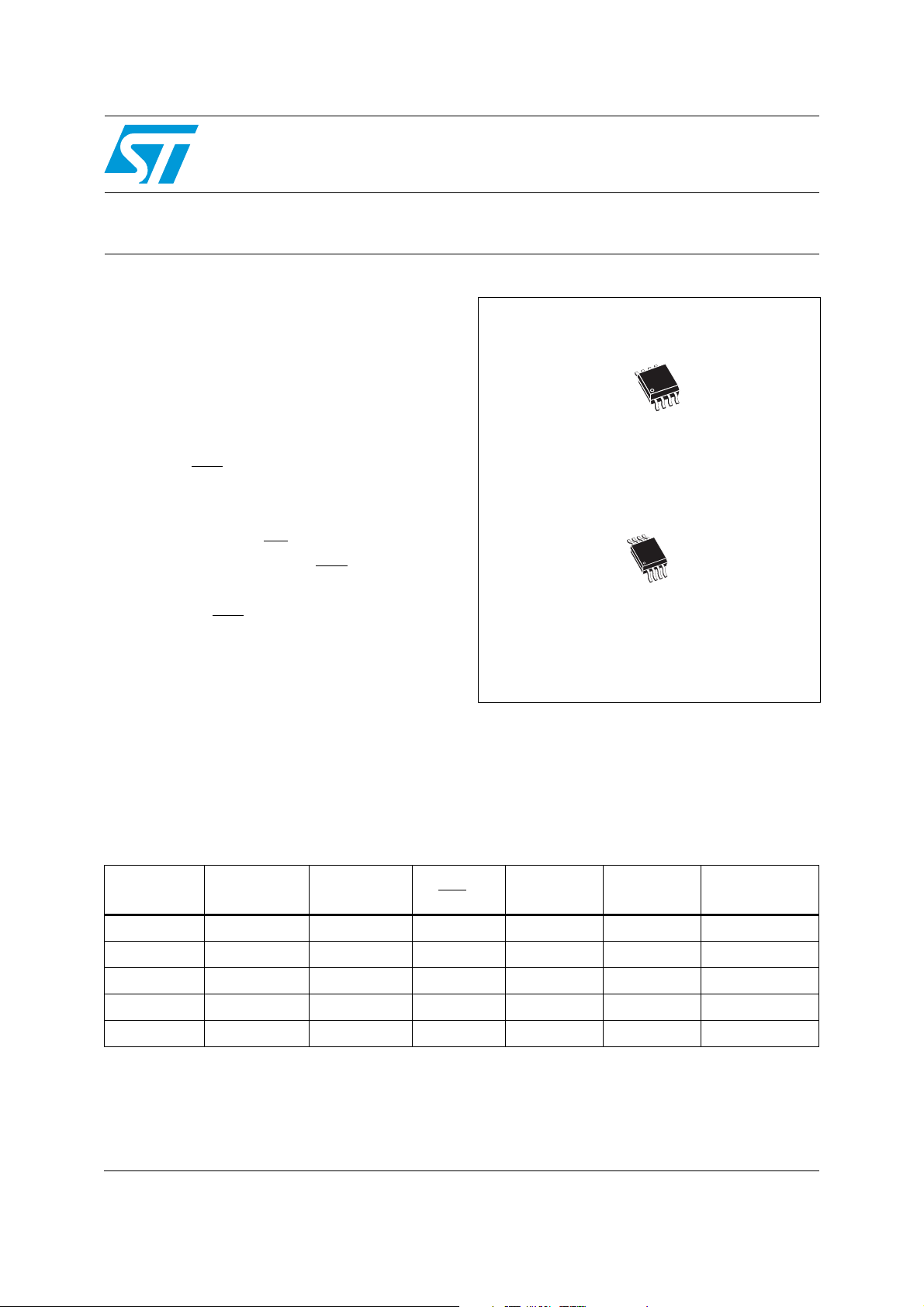
These devices are available in a standard 8-pin SOIC package or a space-saving 8-pin
TSSOP package.
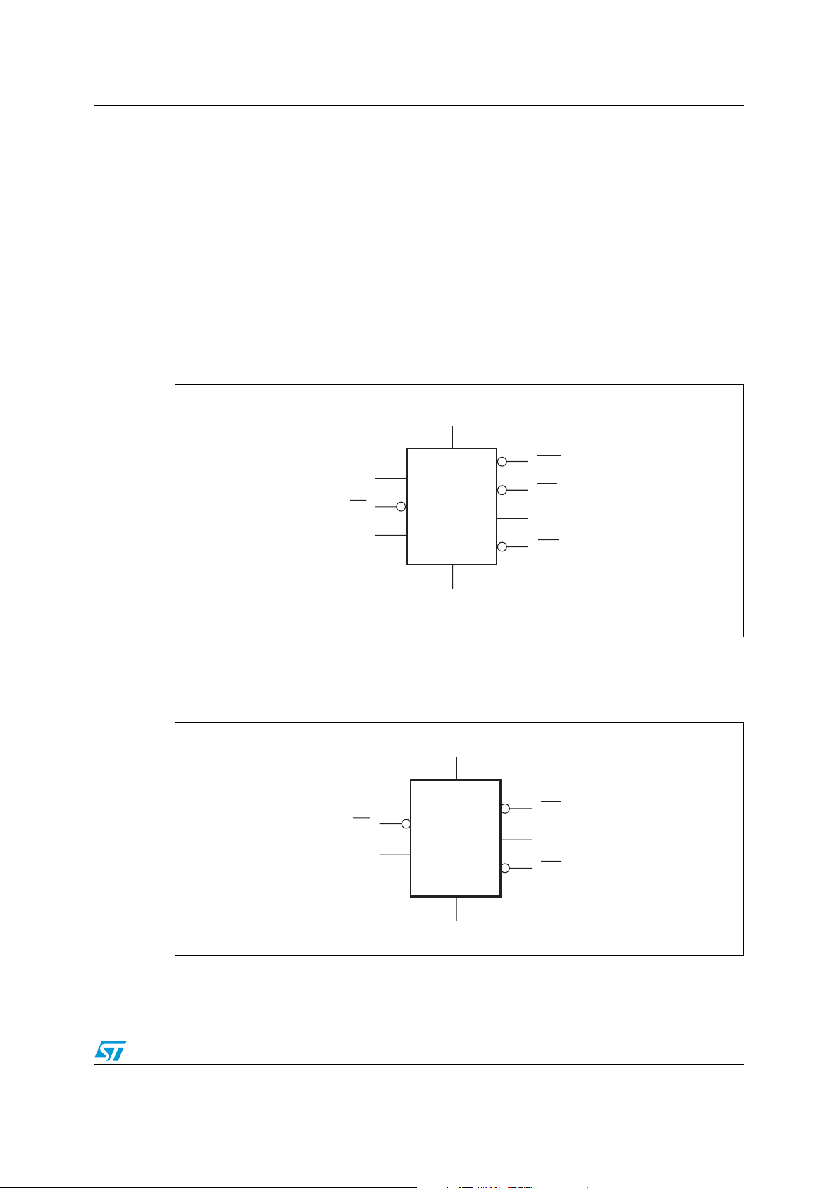
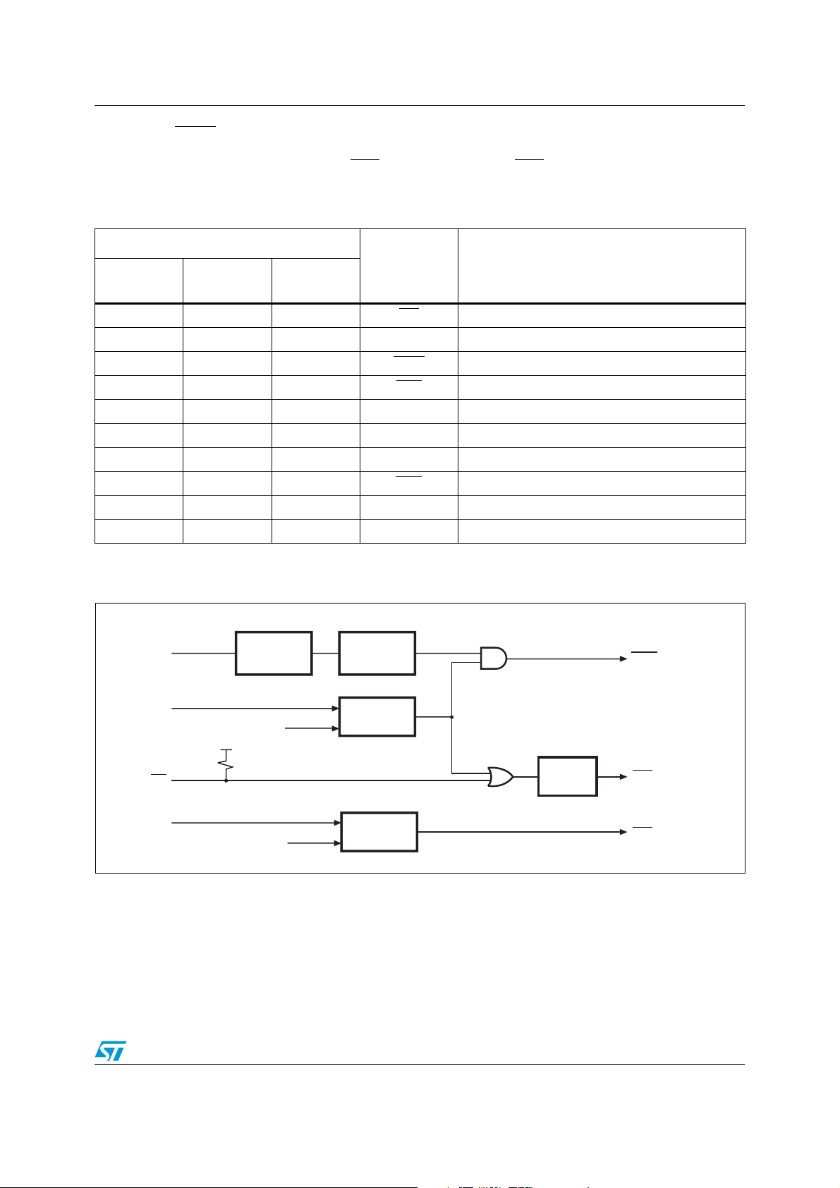
Figure 1. Logic diagram (STM705/706/813L)
input for an out-of-tolerance condition. When an invalid VCC condition
CC
) is forced low (or high in the case of RST).
V
CC
WDO
WDI
MR
PFI
STM705/706;
STM813L
RST
RST
PFO
(1)
(2)
1. For STM705/706 only.
2. For STM813L only.
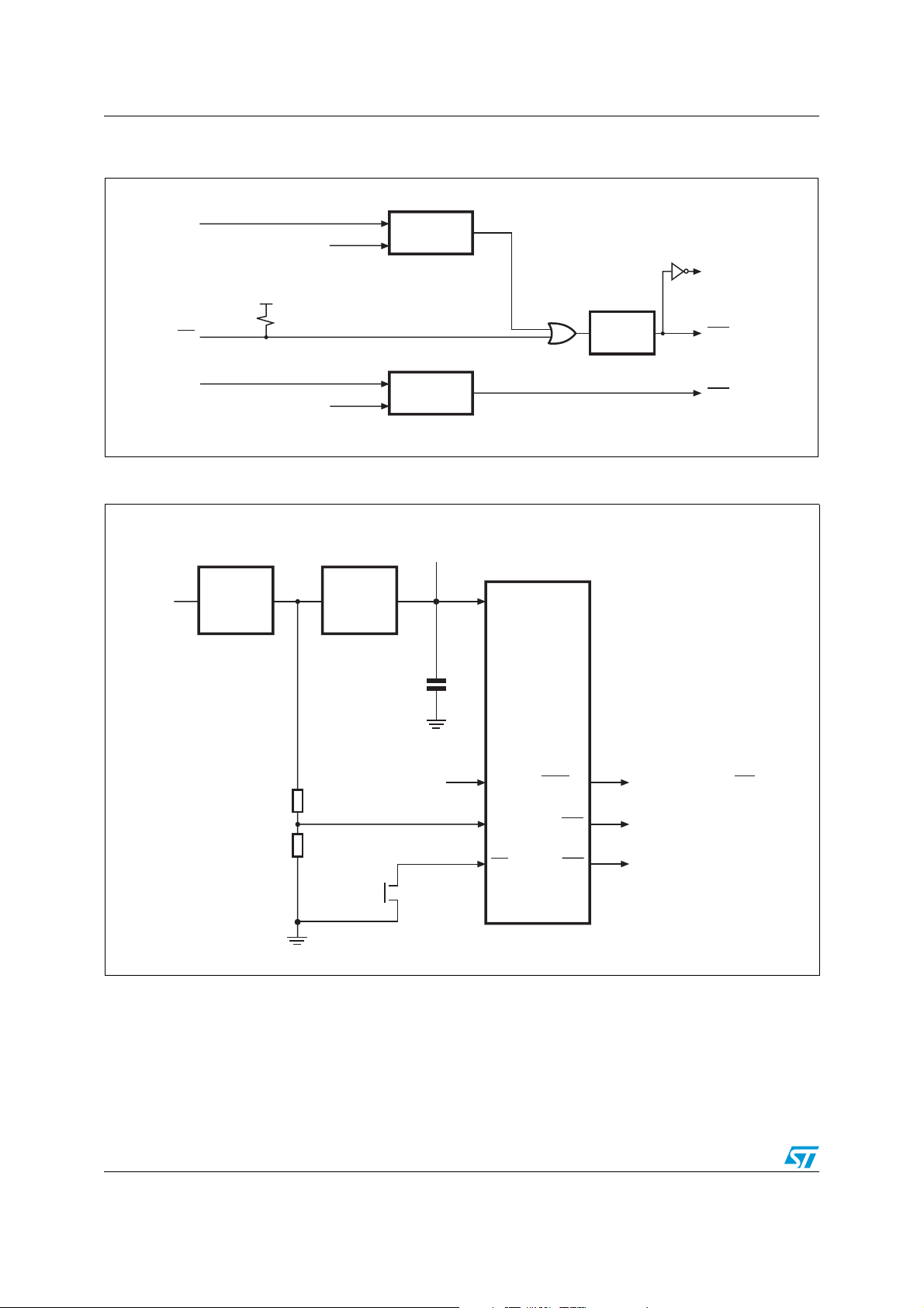
Figure 2. Logic diagram (STM707/708)
MR
STM707/708
PFI
V
SS
AI08825
V
CC
RST
RST
PFO
V
SS
AI08826
Doc ID 10520 Rev 9 5/33
Page 6
Description STM705, STM706, STM707, STM708, STM813L
Table 2. Signal names
MR Push-button reset input
WDI Watchdog input
Watchdog output
WDO
RST
Active-low reset output
(1)
RST
Supply voltage
V
CC
Active-high reset output
PFI Power-fail input
PFO Power-fail output
Ground
V
SS
NC No connect
1. For STM813L only.
Figure 3. STM705/706/813L SO8 connections
SO8
MR
V
CC
V
SS
PFI
1
2
3
4
8
7
6
5
WDO
RST (RST)
WDI
PFO
1. For STM813L, reset output is active-high.
Figure 4. STM705/706/813L TSSOP8 connections
TSSOP8
WDO
MR
V
(1)
CC
(RST) RST
1. For STM813L, reset output is active-high.
1
2
3
4
WDI
8
PFO
7
PFI
6
V
5
(1)
AI08827a
SS
AI09114
6/33 Doc ID 10520 Rev 9
Page 7
STM705, STM706, STM707, STM708, STM813L Description
Figure 5. STM707/708 SO8 connections
SO8
MR
V
CC
V
SS
PFI
1
2
3
4
RST
8
RST
7
NC
6
PFO
5
AI08828a
Figure 6. STM707/708 TSSOP8 connections
TSSOP8
RST
RST
MR
V
CC
1
2
3
4
NC
8
PFO
7
PFI
6
V
5
SS
AI09115
Doc ID 10520 Rev 9 7/33
Page 8

Pin descriptions STM705, STM706, STM707, STM708, STM813L
2 Pin descriptions
2.1 MR
A logic low on MR asserts the reset output. Reset remains asserted as long as MR is low
and for t
driven from a TTL or CMOS logic line, or shorted to ground with a switch. Leave open if
unused.
2.2 WDI
If WDI remains high or low for 1.6 s, the internal watchdog timer runs out and reset
(or WDO
WDI sees a rising or falling edge.
The watchdog function can be disabled by allowing the WDI pin to float.
2.3 WDO
after MR returns high. This active-low input has an internal pull-up. It can be
rec
) is triggered. The internal watchdog timer clears while reset is asserted or when
It goes low when a transition does not occur on WDI within 1.6 s, and remains low until
a transition occurs on WDI (indicating the watchdog interrupt has been serviced). WDO
goes low when V
goes high as soon as V
Note: For those devices with a WDO
is connected to MR
falls below the reset threshold; however, unlike the reset output, WDO
CC
exceeds the reset threshold. Output type is push-pull.
CC
.
2.4 RST
Pulses low when triggered, and stays low whenever VCC is below the reset threshold or
when MR
threshold, or MR
is a logic low. It remains low for t
goes from low to high.
2.5 RST
Goes high with triggered, and stays high whenever VCC is above the reset threshold or
when MR
or MR
is a logic high. It stays high for t
goes from high to low.
2.6 PFI
also
output, a watchdog timeout will not trigger reset unless WDO
after either VCC rises above the reset
rec
after either VCC falls below the reset threshold,
rec
When PFI is less than V
ground if unused.
8/33 Doc ID 10520 Rev 9
, PFO goes low; otherwise, PFO remains high. Connect to
PFI
Page 9
STM705, STM706, STM707, STM708, STM813L Pin descriptions
2.7 PFO
When PFI is less than V
, PFO goes low; otherwise, PFO remains high. Leave open if
PFI
unused. Output type is push-pull.
Table 3. Pin description
STM813L
— 7 7 RST
— 6 — NC No connect
Pin
STM707
STM708
STM705
STM706
1 1 1 MR
Name Function
Push-button reset input
6 — 6 WDI Watchdog input
8 — 8 WDO Watchdog output (push-pull)
Active-low reset output
7 8 — RST Active-high reset output
2 2 2 VCC Supply voltage
4 4 4 PFI Power-fail input
5 5 5 PFO Power-fail output (push-pull)
3 3 3 V
Ground
SS
Figure 7. Block diagram (STM705/706/813L)
WDI
V
CC
MR
PFI
1. For STM813L only.
V
CC
WDI
transitional
detector
V
RST
V
PFI
WATCHDOG
TIMER
COMPARE
COMPARE
t
rec
generator
WDO
RST (RST)
PFO
(1)
AI08829
Doc ID 10520 Rev 9 9/33
Page 10
Pin descriptions STM705, STM706, STM707, STM708, STM813L
Figure 8. Block diagram (STM707/708)
V
CC
MR
V
RST
V
CC
COMPARE
t
rec
generator
RST
RST
PFI
Figure 9. Hardware hookup
Unregulated
voltage
R1
R2
V
CC
COMPARE
0.1 mF
Push-button
V
PFI
Regulator
V
IN
From microprocessor
5 V
V
CC
STM705
STM706
STM707
STM708
STM813L
(1)
WDI
PFI
MR
(1)
WDO
PFO
RST To microprocessor reset
To microprocessor IRQ
To microprocessor NMI
PFO
AI08830
1. For STM705/706/813L.
10/33 Doc ID 10520 Rev 9
AI08831a
Page 11

STM705, STM706, STM707, STM708, STM813L Operation
3 Operation
3.1 Reset output
The STM705/706/707/708/813L supervisor asserts a reset signal to the MCU whenever
V
goes below the reset threshold (V
CC
MR
), or when the push-button reset input (MR) is taken low. RST is guaranteed to be a logic
low (logic high for STM707/708/813L) for V
85 °C.
), a watchdog time-out occurs (if WDO is tied to
RST
CC
< V
down to VCC =1 V for TA = 0 °C to
RST
During power-up, once V
the reset time-out period, t
If V
drops below the reset threshold, RST goes low. Each time RST is asserted, it stays
CC
low for at least the reset time-out period (t
exceeds the reset threshold an internal timer keeps RST low for
CC
. After this interval RST returns high.
rec
). Any time VCC goes below the reset threshold
rec
the internal timer clears. The reset timer starts when V
3.2 Push-button reset input
A logic low on MR asserts reset. Reset remains asserted while MR is low, and for t
Figure 29) after it returns high. The MR
input has an internal 40 Ω pull-up resistor, allowing it
to be left open if not used. This input can be driven with TTL/CMOS-logic levels or with
open-drain/ collector outputs. Connect a normally open momentary switch from MR
to create a manual reset function; external debounce circuitry is not required. If MR
from long cables or the device is used in a noisy environment, connect a 0.1 µF capacitor
from MR
to GND to provide additional noise immunity. MR may float, or be tied to VCC when
not used.
3.3 Watchdog input (STM705/706/813L)
The watchdog timer can be used to detect an out-of-control MCU. If the MCU does not
toggle the Watchdog Input (WDI) within t
timer is cleared by either:
1. a reset pulse, or
2. by toggling WDI (high-to-low or low-to-high), which can detect pulses as short as 50 ns.
If WDI is tied high or low, a reset pulse is triggered every 1.8 s (t
connected to MR
.
(1.6 s), the reset is asserted. The internal 1.6s
WD
returns above the reset threshold.
CC
rec
to GND
is driven
+ t
WD
), if WDO is
rec
(see
See Figure 30 for STM705/706/813L.
The timer remains cleared and does not count for as long as reset is asserted. As soon as
reset is released, the timer starts counting.
Note: The watchdog function may be disabled by floating WDI or tri-stating the driver connected to
WDI. When tri-stated or disconnected, the maximum allowable leakage current is 10 µA and
the maximum allowable load capacitance is 200 pF.
Doc ID 10520 Rev 9 11/33
Page 12

Operation STM705, STM706, STM707, STM708, STM813L
3.4 Watchdog output (STM705/706/813L)
When VCC drops below the reset threshold, WDO will go low even if the watchdog timer has
not yet timed out. However, unlike the reset output, WDO
exceeds the reset threshold. WDO
to the MR
input.
may be used to generate a reset pulse by connecting it
goes high as soon as VCC
3.5 Power-fail input/output
The power-fail input (PFI) is compared to an internal reference voltage (independent from
the V
output (PFO
signal a failing power supply. Typically PFI is connected through an external voltage divider
(see Figure 9) to either the unregulated DC input (if it is available) or the regulated output of
the V
V
PFI
or the microprocessor drops below the minimum operating voltage.
comparator). If PFI is less than the power-fail threshold (V
RST
), the power-fail
PFI
) will go low. This function is intended for use as an undervoltage detector to
regulator. The voltage divider can be set up such that the voltage at PFI falls below
CC
several milliseconds before the regulated VCC input to the STM705/706/707/708/ 813L
If the comparator is unused, PFI should be connected to V
PFO
may be connected to MR on the STM703/704/818 so that a low voltage on PFI will
and PFO left unconnected.
SS
generate a reset output.
3.6 Ensuring a valid reset output down to VCC = 0 V
When VCC falls below 1 V, the state of the RST output can no longer be guaranteed, and
becomes essentially an open circuit. If a high value pulldown resistor is added to the RST
pin, the output will be held low during this condition. A resistor value of approximately
100 kΩ will be large enough to not load the output under operating conditions, but still
sufficient to pull RST
Figure 10. Reset output valid to ground circuit
to ground during this low voltage condition (see Figure 10).
STMXXX
RST
R1
AI08835
12/33 Doc ID 10520 Rev 9
Page 13

STM705, STM706, STM707, STM708, STM813L Operation
3.7 Interfacing to microprocessors with bidirectional reset pins
Microprocessors with bidirectional reset pins can contend with the STM705-708 reset
output. For example, if the reset output is driven high and the micro wants to pull it low,
signal contention will result. To prevent this from occurring, connect a 4.7 kΩ resistor
between the reset output and the micro's reset I/O as in Figure 11.
Figure 11. Interfacing to microprocessors with bidirectional reset I/O
Buffered reset to other
system components
V
CC
STMXXX
GND
RST
4.7 k
V
CC
Microprocessor
RST
GND
AI08836
Doc ID 10520 Rev 9 13/33
Page 14

Typical operating characteristics STM705, STM706, STM707, STM708, STM813L
4 Typical operating characteristics
Typical values are at TA = 25 °C.
Figure 12. Supply current vs. temperature (no load)
30
25
20
15
VCC = 2.7 V
10
Supply current (µA)
5
VCC = 3.0 V
VCC = 3.6 V
VCC = 4.5 V
VCC = 5.5 V
0
–40 –20 0 20 40 60 80 100 120
Figure 13. V
1.270
1.265
1.260
1.255
1.250
threshold (V)
1.245
PFI
V
1.240
1.235
1.230
1.225
Temperature (°C)
threshold vs. temperature
PFI
VCC = 2.5 V
VCC = 3.0 V
VCC = 3.3 V
VCC = 3.6 V
–40 –20 0 20 40 60 80 100 120
Temperature (°C)
AI09141b
AI09142b
14/33 Doc ID 10520 Rev 9
Page 15

STM705, STM706, STM707, STM708, STM813L Typical operating characteristics
Figure 14. Reset comparator propagation delay vs. temperature
30
28
26
24
22
20
18
Propagation delay (µs)
16
14
12
10
–40 –20 0 20 40 60 80 100 120
Temperature (°C)
AI09143b
Figure 15. Power-up t
240
235
230
225
(ms)
rec
t
220
215
210
–40 –20 0 20 40 60 80 100 120
vs. temperature
rec
Temperature (°C)
VCC = 3.0 V
VCC = 4.5 V
VCC = 5.5 V
AI09144b
Doc ID 10520 Rev 9 15/33
Page 16

Typical operating characteristics STM705, STM706, STM707, STM708, STM813L
Figure 16. Normalized reset threshold vs. temperature
1.004
1.002
threshold
reset
1.000
0.998
Normalized
0.996
–40 –20 0 20 40 60 80 100 120
Temperature (°C)
AI09145b
Figure 17. Watchdog time-out period vs. temperature
1.90
1.85
1.80
1.75
1.70
Watchdog time-out period (s)
1.65
1.60
–40 –20 0 20 40 60 80 100 120
Temperature (°C)
VCC = 3.0 V
VCC = 4.5 V
VCC = 5.5 V
AI09146b
16/33 Doc ID 10520 Rev 9
Page 17

STM705, STM706, STM707, STM708, STM813L Typical operating characteristics
Figure 18. PFI to PFO propagation delay vs. temperature
4.0
VCC = 3.0 V
3.0
2.0
1.0
PFI to PFO propagation delay (µs)
0.0
–40 –20 0 20 40 60 80 100 120
Temperature (°C)
VCC = 3.6 V
VCC = 4.5 V
VCC = 5.5 V
AI09148b
Figure 19. Output voltage vs. load current (VCC = 5 V; TA = 25 °C)
5.00
4.98
(V)
OUT
V
4.96
4.94
0 1020304050
I
(mA)
OUT
AI10496
Doc ID 10520 Rev 9 17/33
Page 18

Typical operating characteristics STM705, STM706, STM707, STM708, STM813L
Figure 20. RST output voltage vs. supply voltage
5
4
3
(V)
RST
2
V
1
0
500 ms / div
Figure 21. RST output voltage vs. supply voltage
5
4
V
V
V
V
RST
CC
RST
CC
5
4
3
2
1
0
AI09149b
5
4
(V)
CC
V
(V)
RST
V
3
2
1
0
500 ms / div
3
2
1
0
AI09150b
(V)
CC
V
18/33 Doc ID 10520 Rev 9
Page 19

STM705, STM706, STM707, STM708, STM813L Typical operating characteristics
Figure 22. RST response time (assertion)
1. V
5V
V
CC
5V
RST
= 4.603 V at 25 °C.
RST
5 µs / div
1 V / div
4V
4V
1V/div
0V
AI09151b
Doc ID 10520 Rev 9 19/33
Page 20

Typical operating characteristics STM705, STM706, STM707, STM708, STM813L
Figure 23. RST response time (assertion)
5V
V
CC
1V/div
RST
1V/div
4V
4V
0V
5 µs / div
1. V
= 4.603 V at 25 °C.
RST
Figure 24. Power-fail comparator response time (assertion)
5V
PFO
1.3 V
PFI
AI09152b
1V/div
0V
500 mV / div
500 ns / div
20/33 Doc ID 10520 Rev 9
0V
AI09153b
Page 21

STM705, STM706, STM707, STM708, STM813L Typical operating characteristics
Figure 25. Power-fail comparator response time (de-assertion)
5V
PFO
0V
PFI
0V
500 ns / div
Figure 26. Maximum transient duration vs. reset threshold overdrive
6000
5000
1V/div
1.3 V
500 mV / div
AI09154b
4000
duration (µs)
3000
2000
Transient
1000
0
Reset occurs
above the cur ve
Reset comparator ov erdrive, V
Doc ID 10520 Rev 9 21/33
RST
– VCC (V)
0111.010.0100.0
AI09156b
Page 22

Maximum ratings STM705, STM706, STM707, STM708, STM813L
5 Maximum ratings
Stressing the device above the rating listed in the absolute maximum ratings table may
cause permanent damage to the device. These are stress ratings only and operation of the
device at these or any other conditions above those indicated in the operating sections of
this specification is not implied. Exposure to absolute maximum rating conditions for
extended periods may affect device reliability.
Table 4. Absolute maximum ratings
Symbol Parameter Value Unit
T
STG
T
SLD
V
IO
V
CC
I
O
P
D
1. Reflow at peak temperature of 260 °C. The time above 255 °C must not exceed 30 seconds.
Storage temperature (VCC Off) –55 to 150 °C
(1)
Lead solder temperature for 10 seconds 260 °C
Input or output voltage –0.3 to VCC +0.3 V
Supply voltage –0.3 to 7.0 V
Output current 20 mA
Power dissipation 320 mW
22/33 Doc ID 10520 Rev 9
Page 23

STM705, STM706, STM707, STM708, STM813L DC and AC parameters
6 DC and AC parameters
This section summarizes the operating and measurement conditions, and the DC and AC
characteristics of the device. The parameters in the DC and AC characteristics tables that
follow, are derived from tests performed under the measurement conditions summarized in
Ta bl e 5 . Designers should check that the operating conditions in their circuit match the
operating conditions when relying on the quoted parameters.
Table 5. Operating and AC measurement conditions
V
supply voltage 1.0 to 5.5 V
CC
Ambient operating temperature (T
Input rise and fall times
Input pulse voltages 0.2 to 0.8 V
Input and output timing ref. voltages 0.3 to 0.7 V
Parameter STM705/706/707/708; STM813L Unit
) –40 to 85 °C
A
≤
5 ns
V
CC
V
CC
Figure 27. AC testing input/output waveforms
0.8 V
CC
0.2 V
CC
Figure 28. Power-fail comparator waveform
V
CC
V
RST
PFO
0.7 V
0.3 V
CC
CC
t
AI02568
rec
RST
AI08834b
Doc ID 10520 Rev 9 23/33
Page 24

DC and AC parameters STM705, STM706, STM707, STM708, STM813L
Figure 29. MR timing waveform
MR
t
MLRL
(1)
RST
t
MLMH
1. RST for STM805.
Figure 30. Watchdog timing (STM705/706/813L)
V
CC
t
RST
WDI
WDO
rec
t
rec
t
WD
AI07837a
AI08833
24/33 Doc ID 10520 Rev 9
Page 25

STM705, STM706, STM707, STM708, STM813L DC and AC parameters
Table 6. DC and AC characteristics
Sym Description Test condition
Operating voltage 1.2
V
CC
I
CCVCC
(1)
Min Typ Max Unit
(2)
supply current 25 60 µA
Input leakage current (MR) 4.5 V < VCC < 5.5 V 75 125 300 µA
Input leakage current (PFI) 0 V < VIN < VCC –25 2 +25 nA
I
LI
Input leakage current (WDI)
Input high voltage (MR) 4.5 V < VCC < 5.5 V 2.0 V
V
IH
V
Input high voltage (WDI) V
IH
Input low voltage (MR) 4.5 V < VCC < 5.5 V 0.8 V
V
IL
V
Input low voltage (WDI) V
IL
Output low voltage (PFO
V
OL
RST, WDO
Output low voltage (RST)
V
OL
)
Output high voltage (RST
)
WDO
V
OH
Output high voltage (PFO
, RST,
, RST,
)
VOH Output high voltage (RST)
WDI = VCC, time average 120 160 µA
WDI = GND, time average –20 –15 µA
(max) < VCC < 5.5 V 0.7 VCC V
RST
(max) < VCC < 5.5 V 0.3 VCC V
RST
V
CC
I
= V
I
SINK
I
SINK
SOURCE
RST
(max), I
= 3.2 mA 0.3 V
SINK
= 50 µA, VCC = 1.0 V,
= 0 °C to 85 °C
T
A
= 100 µA, VCC = 1.2 V 0.3 V
I
SOURCE
V
I
SOURCE
VCC = V
CC
= V
= 1 mA,
(max)
RST
= 75 µA,
(max)
RST
2.4 V
0.8 V
V
CC
= 4 µA, VCC = 1.1 V,
TA = 0 °C to 85 °C
I
SOURCE
= 4 µA, VCC = 1.2 V 0.9 V
Power-fail comparator
5.5 V
0.3 V
0.8 V
PFI input threshold PFI falling (VCC = 5 V) 1.20 1.25 1.30 V
V
PFI
t
PFI to PFO propagation delay 2 µs
PFD
Doc ID 10520 Rev 9 25/33
Page 26

DC and AC parameters STM705, STM706, STM707, STM708, STM813L
Table 6. DC and AC characteristics
Sym Description Test condition
Reset thresholds
(1)
Min Typ Max Unit
Reset threshold
V
RST
(3)
STM705/707/813L 4.50 4.65 4.75 V
STM706/708 4.25 4.40 4.50 V
Reset threshold hysteresis 25 mV
RST pulse width
t
rec
Blank (see Ta bl e 9 ) 140 200 280
A (see Ta bl e 9 ) 160 200 280
Push-button reset input
t
MLMH
(or tMR)
t
(
MR pulse width 150 ns
MLRL
MR to RST output delay 250 ns
t
MRD)
Watchdog timer (STM705/706/813L)
Watchdog timeout period 4.5 V < VCC < 5.5 V 1.12 1.60 2.24 s
t
WD
WDI pulse width 4.5 V < VCC < 5.5 V 50 ns
1. Valid for ambient operating temperature: TA = –40 to 85 °C; VCC = 4.75 V to 5.5 V for STM705/707/813L;
VCC = 4.5 V to 5.5 V for STM706/708 (except where noted).
(min) = 1.0 V for TA = 0 °C to +85 °C.
2. V
CC
3. For V
CC
falling.
ms
26/33 Doc ID 10520 Rev 9
Page 27

STM705, STM706, STM707, STM708, STM813L Package mechanical data
7 Package mechanical data
In order to meet environmental requirements, ST offers these devices in different grades of
ECOPACK
specifications, grade definitions and product status are available at: www.st.com.
ECOPACK
®
packages, depending on their level of environmental compliance. ECOPACK®
®
is an ST trademark.
Doc ID 10520 Rev 9 27/33
Page 28

Package mechanical data STM705, STM706, STM707, STM708, STM813L
Figure 31. SO8 – 8-lead plastic small outline, 150 mils body width, outline
A2
A
C
B
e
ddd
D
8
E
H
1
1. Drawing is not to scale.
LA1
SO-A
Table 7. SO8 - 8-lead plastic small outline, 150 mils body width, pack. mech. data
mm inches
Symbol
Typ Min Max Typ Min Max
A — 1.35 1.75 — 0.053 0.069
A1 — 0.10 0.25 — 0.004 0.010
B — 0.33 0.51 — 0.013 0.020
C — 0.19 0.25 — 0.007 0.010
D — 4.80 5.00 — 0.189 0.197
ddd — — 0.10 — — 0.004
E — 3.80 4.00 — 0.150 0.157
e 1.27 — — 0.050 — —
H — 5.80 6.20 — 0.228 0.244
h — 0.25 0.50 — 0.010 0.020
L — 0.40 0.90 — 0.016 0.035
α — 0° 8° — 0° 8°
N 8 8
28/33 Doc ID 10520 Rev 9
Page 29

STM705, STM706, STM707, STM708, STM813L Package mechanical data
Figure 32. TSSOP8 – 8-lead, thin shrink small outline, 3 x 3 mm body size, outline
D
8
1
CP
1. Drawing is not to scale.
5
EE1
4
A1
A2A
eb
L
L1
Table 8. TSSOP8 - 8-lead, thin shrink small outline, 3 x 3 mm body size,
mechanical data
mm inches
Symbol
Typ Min Max Typ Min Max
c
TSSOP8BM
A — — 1.10 — — 0.043
A1 — 0.05 0.15 — 0.002 0.006
A2 0.85 0.75 0.95 0.034 0.030 0.037
b — 0.25 0.40 — 0.010 0.016
c — 0.13 0.23 — 0.005 0.009
CP — — 0.10 — — 0.004
D 3.00 2.90 3.10 0.118 0.114 0.122
e 0.65 — — 0.026 — —
E 4.90 4.65 5.15 0.193 0.183 0.203
E1 3.00 2.90 3.10 0.118 0.114 0.122
L 0.55 0.40 0.70 0.022 0.016 0.030
L1 0.95 — — 0.037 — —
α — 0° 6° — 0° 6°
N 8 8
Doc ID 10520 Rev 9 29/33
Page 30

Part numbering STM705, STM706, STM707, STM708, STM813L
8 Part numbering
Table 9. Ordering information scheme
Example: STM705 M 6 E
Device type and reset threshold voltage
STM705/707/813L = V
STM706/708 = V
RST
pulse width
RST
Blank = 140 to 280 ms
(1)
= 160 to 280 ms
A
Package
M = SO8
(2)
DS
= TSSOP8
= 4.50 V to 4.75 V
RST
= 4.25 V to 4.50 V
Temperature range
6 = –40 to 85 °C
Shipping method
E = ECOPACK
®
package, tubes
F = ECOPACK® package, tape and reel
1. Available for STM706/708 in SO8 (M) package only.
2. Contact local ST sales office for availability.
For other options, or for more information on any aspect of this device, please contact the
ST sales office nearest you.
Table 10. Marking description
Part number Reset threshold Package Topside marking
STM705 4.63 V
STM706 4.38 V
STM707 4.63 V
STM708 4.38 V
STM813L 4.63 V
SO8
TSSOP8
SO8
TSSOP8
SO8
TSSOP8
SO8
TSSOP8
SO8
TSSOP8
705
706
707
708
813L
30/33 Doc ID 10520 Rev 9
Page 31

STM705, STM706, STM707, STM708, STM813L Revision history
9 Revision history
Table 11. Document revision history
Date Revision Changes
Sep-2003 1 Initial release.
31-Oct-2003 1.1 Update Ta bl e 6 .
12-Dec-2003 2
16-Jan-2004 2.1 Add typical characteristics (Figure 12 to 18, 20 to 26)
09-Apr-2004 3
25-May-2004 4 Update characteristics (Ta b le 4 , 7)
02-Jul-2004 5 Document promoted; corrected waveform (Figure 28)
Reformatted; update characteristics (Figure 1, 2, 3, 4, 6, 8, 9, 10, 28;
29, 30, Ta bl e 7 , 9, 11)
Reformatted; update characteristics (Figure 14, 18, 20 to 23, 26;
Ta bl e 7 )
21-Sep-2004 6
Clarify root part numbers, pin descriptions (Figure 2, 3, 10; Ta b le 6 , 7,
10)
08-Mar-2005 7 Update typical characteristics (Figure 12 to 26)
02-Nov-2009 8 Updated Ta b le 1 , 3, 4, 6, 9, Section 2.3, Section 2.7, text in Section 7.
06-Aug-2010 9 Updated Features, Section 4: Typical operating characteristics,Ta bl e 9 .
Doc ID 10520 Rev 9 31/33
Page 32

STM705, STM706, STM707, STM708, STM813L
Please Read Carefully:
Information in this document is provided solely in connection with ST products. STMicroelectronics NV and its subsidiaries (“ST”) reserve the
right to make changes, corrections, modifications or improvements, to this document, and the products and services described herein at any
time, without notice.
All ST products are sold pursuant to ST’s terms and conditions of sale.
Purchasers are solely responsible for the choice, selection and use of the ST products and services described herein, and ST assumes no
liability whatsoever relating to the choice, selection or use of the ST products and services described herein.
No license, express or implied, by estoppel or otherwise, to any intellectual property rights is granted under this document. If any part of this
document refers to any third party products or services it shall not be deemed a license grant by ST for the use of such third party products
or services, or any intellectual property contained therein or considered as a warranty covering the use in any manner whatsoever of such
third party products or services or any intellectual property contained therein.
UNLESS OTHERWISE SET FORTH IN ST’S TERMS AND CONDITIONS OF SALE ST DISCLAIMS ANY EXPRESS OR IMPLIED
WARRANTY WITH RESPECT TO THE USE AND/OR SALE OF ST PRODUCTS INCLUDING WITHOUT LIMITATION IMPLIED
WARRANTIES OF MERCHANTABILITY, FITNESS FOR A PARTICULAR PURPOSE (AND THEIR EQUIVALENTS UNDER THE LAWS
OF ANY JURISDICTION), OR INFRINGEMENT OF ANY PATENT, COPYRIGHT OR OTHER INTELLECTUAL PROPERTY RIGHT.
UNLESS EXPRESSLY APPROVED IN WRITING BY AN AUTHORIZED ST REPRESENTATIVE, ST PRODUCTS ARE NOT
RECOMMENDED, AUTHORIZED OR WARRANTED FOR USE IN MILITARY, AIR CRAFT, SPACE, LIFE SAVING, OR LIFE SUSTAINING
APPLICATIONS, NOR IN PRODUCTS OR SYSTEMS WHERE FAILURE OR MALFUNCTION MAY RESULT IN PERSONAL INJURY,
DEATH, OR SEVERE PROPERTY OR ENVIRONMENTAL DAMAGE. ST PRODUCTS WHICH ARE NOT SPECIFIED AS "AUTOMOTIVE
GRADE" MAY ONLY BE USED IN AUTOMOTIVE APPLICATIONS AT USER’S OWN RISK.
Resale of ST products with provisions different from the statements and/or technical features set forth in this document shall immediately void
any warranty granted by ST for the ST product or service described herein and shall not create or extend in any manner whatsoever, any
liability of ST.
ST and the ST logo are trademarks or registered trademarks of ST in various countries.
Information in this document supersedes and replaces all information previously supplied.
The ST logo is a registered trademark of STMicroelectronics. All other names are the property of their respective owners.
© 2010 STMicroelectronics - All rights reserved
STMicroelectronics group of companies
Australia - Belgium - Brazil - Canada - China - Czech Republic - Finland - France - Germany - Hong Kong - India - Israel - Italy - Japan -
Malaysia - Malta - Morocco - Philippines - Singapore - Spain - Sweden - Switzerland - United Kingdom - United States of America
www.st.com
Doc ID 10520 Rev 9 33/33
 Loading...