

Page 1
SATELLITE COMMUNI CATI ONS APPLI CATION S
.SA TE L LITE COMMUNICAT I ONS
AMPLIFIER
.1625 - 1665 MHz
.18/28 VOLTS
.INPUT/OUTPUT 50 OHMS
.P
= 10 W MIN.
OUT
.GAIN = 30 dB MIN.
STM1645-10
RF POWER MODULES
PRELIMINARY DATA
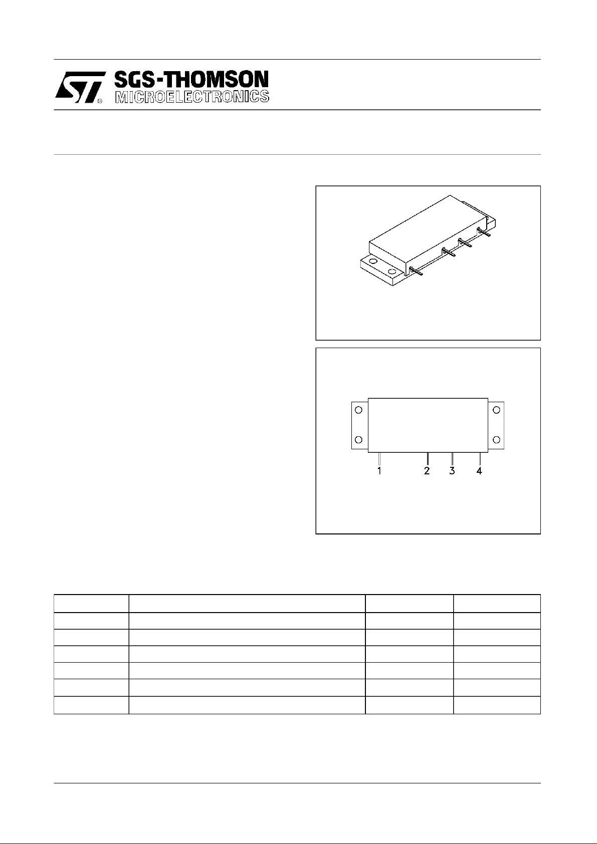
CASE STYLE H150
ORDERCOD E
STM1645-10
PI N C O NNECTION
BRANDING
STM1645-10
DESCRIP TION
The STM1645-10 module is des igned for high
power satellite communication applications in
the 1.6 GHz f requency r ange operating at 28
Volts.
ABSOLUTE MAXI MUM RATI NGS (T
Symbol Parameter Value Unit
P
T
V
V
P
OUT
STG
T
C1
C2
IN
C
DC Supp ly Voltage 20 Vdc
DC Supp ly Voltage 32 Vdc
RF Input Power 20 mW
RF Out put Po we r 16 W
Storage Temperature
Operating Case Temperature
case
=
25°C)
1. RF Input 2. VC1, 18V
3. V
, 28V 4. RF Output
C2
− 40 to +100
− 35 t o +70
°
C
°
C
April 4, 1996
1/5
Page 2
STM 1645-10
ELECTRICAL SPECIFICATIONS (T
Symbol Parameter Test Conditions
case
=25°C, V
=18V,VC2=28V)
C1*
Value
Min. Typ. Max.
BW Frequency Range 1625 — 1665 MHz
— — 10.0 dBm
30 — — dB
30 35 — %
—
−45 −40
No Degradation in Outp ut
Power
G
IN
P
η
Input Power
Power Gain
Efficiency
P
H Harmonics
Z
Input Impedance
IN
— Load Mismatch
*Note: VC1= 18V Regulat ed ± 1%
P
P
P
P
P
10 W
=
OUT
= 10 W
OUT
= 10 W
OUT
10 W reference
=
OUT
= 10 W ZG,ZL=50Ω — 1.5 :1 2.0: 1 VSWR
OUT
VSWR = 10:1 V = 28 Vdc
P
= 10 W
OUT
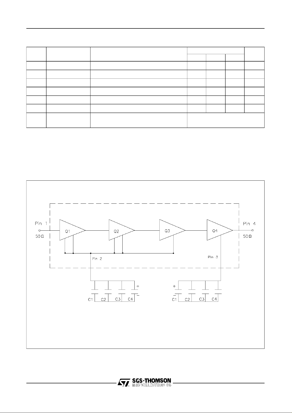
D.C. TEST FIXTURE BYPASSING
Unit
dBc
2/5
C1 : 100pf Chip Capacitor
C2 : 1000pf Chip Capacitor
C3 : .01µf Chip Capacitor
C4 : 10µf Chip Capacitor
Page 3

TYPICAL PERFORMANCE
STM 1645-10
POWER OUTPUT vs FREQUENCY
20
Pin = 10mW
Vc1 = 18V
Vc2 = 28V
18
16
14
Power Output (Watts)
12
10
1620 1625 1630 1635 1640 1645 1650 1655 1660 1665 1670
Frequency (MHz)
-35 deg C
+25 deg C
+70 deg C
VC2 vs FLANGE TEMPERATURE
30
Vc1 = 18V
Pin = 10mW
28
Pout = 10W
26
24
Vc2 (Volts)
22
20
0 10203040506070800-10-20-30-40
Temperature(Deg C)
1662 MHz
1626 MHz
3/5
Page 4

STM 1645-10
APPLI CATI O NS RECOMMENDATIONS
OPERATION LIMITS
The STM1645-10 power module should never be
operated under any condition which exceeds the
Absolute Maximum Ratings presented on this
data sheet. Nor should the module be operated
continuously at any of the specified maximum ratings. If the module is to be subjected to one or
more of the maximum rating conditions, care must
be taken to monitor other parameters which may
be affected.
DECOUPLING
Failure to properly decouple any of the voltage
supply pins mayl result in oscillations at certain
operating frequencies. Therefore, it is recommended that these pins be bypassed as indicated
in the Module DC and Test Fixture Configuration
drawing of this data sheet.
POWER CONTROL
The recommeded method of power control for the
STM1645-10 is to set P
and V
= 28 volts nominal at a flange tempera-
C2
= 10mW, VC1= 18V
IN
ture of 25°C to achieve an output power of 10
watts. Varing V
will allow stable power control
C2
over a wide range of flange temperature. The current consumption of V
is typically 850mA to
C2
900mA for 10 watts power ouput.
MODULE MOUNTING
To insure adequate thermal transfer from the
module to the heatsink, it is recommended that a
satisfactory thermal compound such as Dow
Corning 340, Wakefield 120-2 or equivalent be
applied between the module flange and the
heatsink.
The heatsink mounting surface under the module
should be flat to within ± 0.05mm (± 0.002 inch).
The module should be mounted to the heatsink
using 3 mm (or 4-40) or equivalent screws torqued to 5-6 kg-cm (4-6 in-lb).
The module leads should be attached to equipment PC board using 180°C solder applied to the
leads with a properly grounded soldering iron tip,
not to exceed 195°C, applied a minimum of 2mm
(0.080 inch) from the body of the module for a
duration not to exceed 15 seconds per lead. It is
imperative that no other portion of the module,
other than the leads, be subjected to temperatures in excess of 100°C (maximum storage tem-
perature), for any period of time, as the plastic
moulded cover, internal components and sealing
adhesives may be adversely affected by such
conditions.
Due to the construction techniques and materials
used within the module, reflow soldering of the
flange heatsink or leads, is not recommended.
4/5
Page 5

PACKAGE MECHANICAL DATA
Ref.: Dwg. No. 1018019 rev. D
STM 1645-10
Inform ation f urnished is believed to be accurate a nd reliable. However, SGS - THOMSON Mi cr oel ec t r oni c s assumes no responsibi l ity for
the consequences of use of su ch information nor for any i nf r ingement of patents or other r ights of third parti es which may result from
its use. No license is granted by implication or ot her w ise under any patent or pat ent rights o f S G S - T H O M S O N Microe le ctronics.
Specifications ment i oned in this publicati on ar e subject to change without notice. This publicat ion super s edes and r eplaces all
infor m at i on previously suppl i ed. S GS - THOMS ON M icroelectr onics products ar e not aut hor i zed for use as cr itical com ponents in li f e
support d evices or s ystems wit hout express written approval of SG S - THOMSON M icroelectr oni c s.
1996 S GS-THOM SON Microelectronics - All Right s Reserved
Austr alia - B razil - France - Germ any - H ong K ong - Italy - Japan - K orea - Malaysia -
Mal t a - Mor occo - The N et her lands - Singapore - Spai n - S w eden - Swit zer l and - T ai wan -
SGS-THOMSON Microelectronics GROUP OF COMPANIES
T hai land - U nited Ki ngdom - U.S.A.
5/5
 Loading...