

Datasheet STLVDS9637BDR, STLVDS9637BD, STLVDS3486BTR, STLVDS3486BD, STLVDS3486BDR Datasheet (SGS Thomson Microelectronics)
...Page 1
1/13May 2003
■ MEETS OR EXCEEDS THE
REQUIREMENTS OF ANSI TIA/EIA-644
STANDARD
■ OPERATES WITH A SINGLE 3.3V SUPPLY
■ DESIGNED FOR SIGNA LING RATE UP TO
400Mbps
■ DIFFERENTIAL INPUT THRESHOLDS
±100mV MAX
■ TYPICAL PROPAGATION DELAY TIME OF
2.5ns
■ POWER DISSIPATION 60mW TYPICAL PER
RECEIVER AT 200MHz
■ LOW VOLATGE TTL (LVTTL) LOGIC
OUTPUT LEVELS
■ PIN COMPATIBLE WITH THE AM26LS32,
SN65LVD32
■ OPEN CIRCUIT FAIL SAFE
■ ESD PROTECTION:
7KV RECEIVER PINS
3KV ALL PINS VS GND
DESCRIPTION
The STLVDS32 is a differential line receiver that
implements the electrical characteristics of low
voltage differential signaling (LVDS). This
signaling technique lowers the output voltage
levels of 5V differential standard levels (such as
TIA/EIA-422B) to reduce t he power, increase the
switching speeds and allow operationswith a 3.3V
supply rail. This differential receiver provides a
valid logical output s tate with a 3.3V supply rail. It
also provides a valid logi cal output st ate with a
±100mV differential input voltage within the input
common mode voltage range. The input common
mode voltage allows 1V of ground potential
difference between two LVDS nodes .
The intended application of this device and
signalling technique is both point-to-point and
multidrop data transmission over controlled
impedance media approximately 100Ω.The
transmission media may be printed circuit board
traces, backplanes or cables. The ultim ate rat e
and distance of data transfer depend upon the
attenuation characte ristics of the media and noise
coupling to the environment.
The STLVDS32 v ers ion is characterized for
operation from -4 0°C to 85°C.
ORDERING CODES
Type
Temperature
Range
Package Comments
STLVDS32BD -40 to 85 °C SO-16 (Tube) 50parts per tube / 20tube per box
STLVDS32BDR -40 to 85 °C SO-16 (Tape & Reel) 2500 parts per reel
STLVDS32BTR -40 to 85 °C TSSOP16 (Tape & Reel) 2500 parts per reel
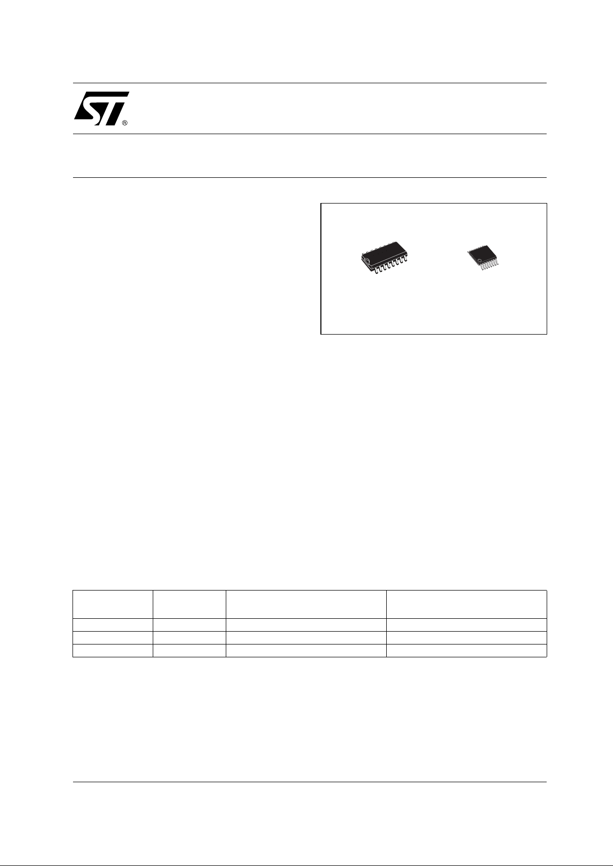
STLVDS32
HIGH SPEED
DIFFERENTIAL LINE RECEIVERS
SOP TSSOP
Page 2
STLVDS32
2/13
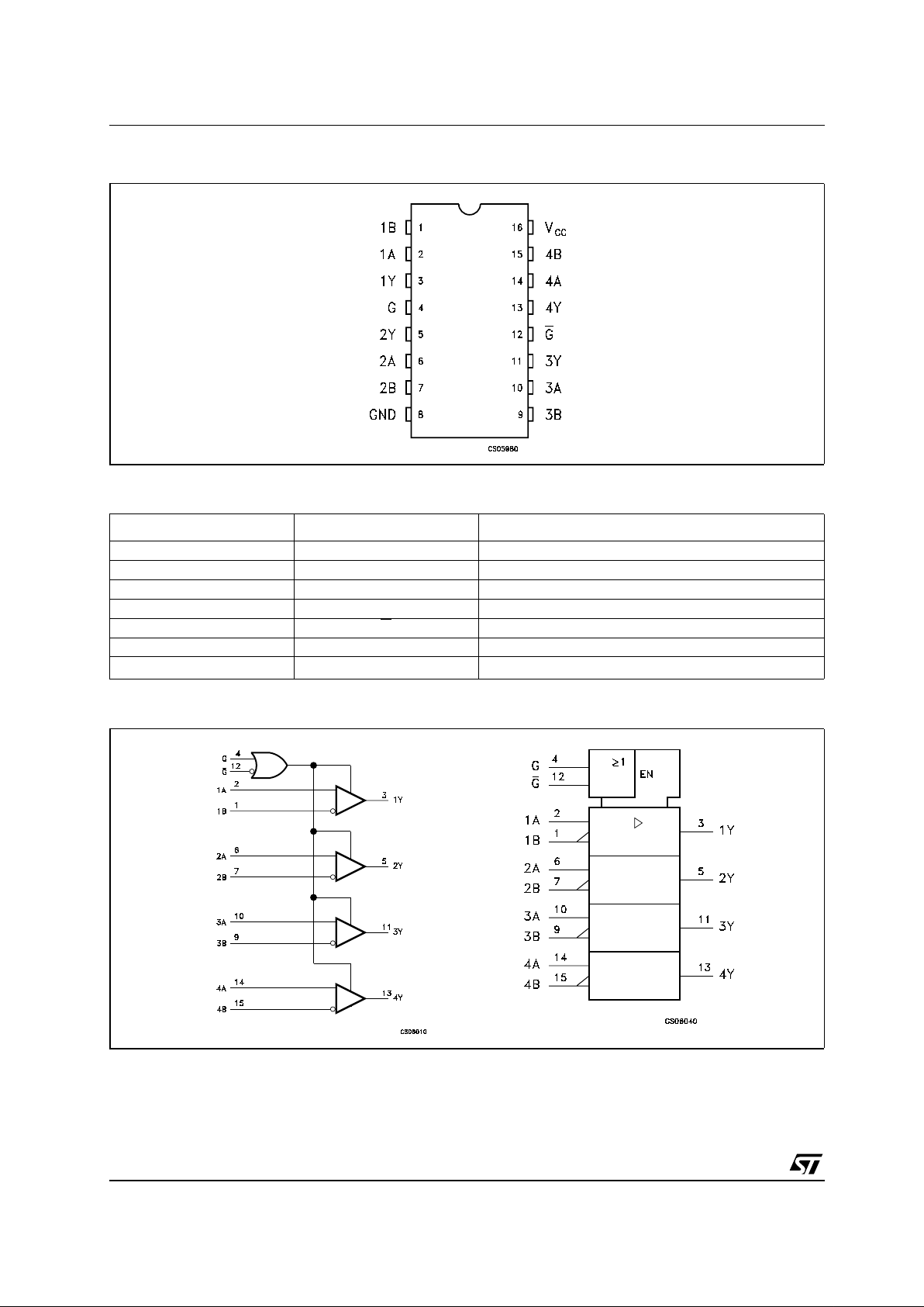
PIN CONFIGURATION
PIN DESCRIPTION
LOGIC DIAGRAM AND LOGIC SYMBOL
PlN N° SYMBOL NAME AND FUNCTION
2, 6, 10, 14 1A to 4A Receiver Inputs
1, 7, 9, 15 1B to 4B Negated Receiver Inputs
3, 5, 11, 13 1Y to 4Y Receiver Outputs
4 G Enable
12 G
Enable
8 GND Ground
16
V
CC
Supply Voltage
Page 3
STLVDS32
3/13
TRUTH TABLE
L = Low level, H = High Level, X = Don’t care, Z = High Impedance,? = Indeterminate
ABSOLUTE MAXIMUM RATINGS
Absolute Maximum Ratings are those values beyond which damage to the device may occur. Functional operation under these condition is
not implied.
Note 1: All voltages except differential I/O bus voltage, are with respect to the network ground terminal.
RECOMMENDED OPERATING CONDITIONS
DIFFERENTIAL INPUTS ENABLES OUTPUT
A, B G G
Y
V
ID
≥ 100mV
HX H
XL H
-100mV < V
ID
< 100mV
HX ?
XL ?
V
ID
≤ -100mV
HX L
XL L
XLHZ
OPEN
HX H
XL H
Symbol Parameter Value Unit
V
CC
Supply Voltage (Note 1)
-0.5 to 4.6 V
V
I
Input Voltage -0.5 to (VCC+ 0.5)
V
V
I
Input Voltage (A or B inputs)
-0.5 to 4.6 V
ESD
Human Body Model Pins Receivers 7
KV
All Pins vs GND 3
T
stg
Storage Temperature Range
-65 to +150 °C
Symbol Parameter Min. Typ. Max. Unit
V
CC
Supply Voltage 3.0 3.3 3.6 V
V
IH
HIGH Level Input Voltage (ENABLE) 2.0 V
V
IL
LOW Level Input Voltage (ENABLE) 0.8 V
|V
ID
| Magnitude of Differential Input Voltage 0.1 0.6 V
V
IC
Common Mode Input Voltage 0.5|VID| 2.4-0.5|VID|V
V
CC
- 0.8
T
A
Operating Temperature Range
-40
85
°C
Page 4
STLVDS32
4/13
ELECTRICAL CHARACTERISTICS (Over recommended operating conditions unless otherwise noted.
All typical values are at T
A
= 25°C, and VCC=3.3V)
Symbol Parameter Test Conditions Min. Typ. Max. Unit
V
ITH+
Positive Going Differential
Input Voltage Threshold
100 mV
V
ITH-
Negative Going Differential
Input Voltage Threshold
-100 mV
V
OH
High Level Output Voltage IOH= -8mA 2.4 V
I
OH
=-4mA 2.8
V
OL
Low Level Output Voltage IOH= 8mA 0.4 V
I
CC
Supply Current for
STLVDS32, STLVDS3486
Enabled, No Load 10 18 mA
Disabled 0.25 0.5 mA
I
CC
Supply Current for
STLVDS9637
No Load 4 10 mA
I
I
Input Current (A or B inputs) VI= 0V -2 -10 -20 µA
V
I
= 2.4V -1.2 -3
I
I(OFF)
Power off Input Current (A
or B inputs)
VCC=0 VI= 3.6V 10 20 µA
I
IH
High Level Input Current
(EN, G, G
or Inputs)
V
IH
=2V 10 µA
I
IL
Low Level Input Current
(EN, G, G
or Inputs)
V
IL
= 0.8V 10 µA
I
OZ
High Impedance Output
Current
VO= 0 or V
CC
± 10 µA
Page 5

STLVDS32
5/13
SWITCHING CHARACTERISTICS (Unless otherwise noted. Typical values are referred to TA=25°C
and V
CC
=3.3V)
Note 1: t
sk(O)
is the maximum delay time difference between the propagation delay of one channel and that of the others on the same chip
with any event on the inputs.
Note2:t
sk(P)
is the magnitude difference in differential propagation delay time between the positive going edge and the negative going edge
of the same channel.
Note 3: t
sk(PP)
is the differential channel-to-channel skew of any event between devices. This specification applies to devices at the same
V
CC
, and within 5°C of each other within the operating temperature range.
Symbol Parameter Test Conditions Min. Typ. Max. Unit
t
PLH
Propagation Delay Time,
Low to High Output
CL= 10pF Fig. 1 1.5 2.5 3.3 ns
t
PHL
Propagation Delay Time,
High to Low Output
1.5 2.5 3.3 ns
t
r
Differential Output Signal
Rise Time
0.4 ns
t
f
Differential Output Signal
Fall Time
0.4 ns
t
sk(O)
Channel to Channel Output
Skew (note1)
0.1 0.3 ns
t
sk(P)
Pulse Skew (|t
PHL-tPLH
|)
(note2)
0.2 0.4 ns
t
sk(PP)
Part to Part Skew (note3) 1 ns
t
PZH
Propagation Delay Time,
High Impedance to High
Level Output
Fig. 2 3 12 ns
t
PZL
Propagation Delay Time,
High Impedance to Low
Level Output
512ns
t
PHZ
Propagation Delay Time,
High Level to High
Impedance Output
512ns
t
PLZ
Propagation Delay Time,
Low Level to High
Impedance Output
512ns
Page 6

STLVDS32
6/13
Figure 1 : Timing Test Circuit, Ti mi ng And Waveforms
Note A: All input pulse are supplied by a generator having the following characteristics: tror tf≤ 1ns, pulse repetition rate (PRR) = 50Mpps,
pulsewidth = 10 ± 0.2ns.
Note B: C
L
includes instrumentation and fixture capacitance within 6mm of the D.U.T.
Page 7

STLVDS32
7/13
Figure2 : Enable And Disable Time TestCircuit And Waveform
Note A: All input pulse are supplied by a generator having the following characteristics: tror tf≤ 1ns, pulse repetition rate (PRR) = 50Mpps,
pulse width = 500 ± 10ns.
Note B:C
L
includes instrumentation andfixture capacitance within 6mmofthe D.U.T.
Page 8

STLVDS32
8/13
TYPICAL PERFORMANCE CHARACTE RISTICS (unless otherwise specified Tj=25°C)
Figure3 : Output Current vs Output Voltage Figure 4 : Output Current vs Out put Voltage
Page 9

STLVDS32
9/13
DIM.
mm. inch
MIN. TYP MAX. MIN. TYP. MAX.
A 1.75 0.068
a1 0.1 0.2 0.004 0.008
a2 1.65 0.064
b 0.35 0.46 0.013 0.018
b1 0.19 0.25 0.007 0.010
C 0.5 0.019
c1 45˚ (typ.)
D 9.8 10 0. 385 0.393
E 5.8 6.2 0.228 0.244
e 1.27 0.050
e3 8.89 0.350
F 3.8 4.0 0.149 0.157
G 4.6 5.3 0.181 0.208
L 0.5 1. 27 0. 019 0.050
M 0.62 0.024
S8 ˚ (max.)
SO-16 MECHANICAL DATA
PO13H
Page 10

STLVDS32
10/13
DIM.
mm. inch
MIN. TYP MAX. MIN. TYP. MAX.
A 1.2 0.047
A1 0.05 0.15 0.002 0.004 0.006
A2 0.8 1 1.05 0.031 0.039 0.041
b 0.19 0.30 0.007 0.012
c 0.09 0.20 0.004 0.0079
D 4.9 5 5.1 0.193 0.197 0.201
E 6.2 6.4 6.6 0.244 0.252 0.260
E1 4.3 4.4 4.48 0.169 0.173 0.176
e 0.65 BSC 0.0256 BSC
K0˚ 8˚0˚ 8˚
L 0.45 0.60 0.75 0.018 0.024 0.030
TSSOP16 MECHANICAL DATA
c
E
b
A2
A
E1
D
1
PIN 1 IDENTIFICATION
A1
L
K
e
0080338D
Page 11

STLVDS32
11/13
DIM.
mm. inch
MIN. TYP MAX. MIN. TYP. MAX.
A 330 12.992
C 12.8 13.2 0.504 0.519
D 20.2 0.795
N 60 2.362
T 22.4 0.882
Ao 6.45 6.65 0.254 0.262
Bo 10.3 10.5 0.406 0.414
Ko 2.1 2.3 0.082 0.090
Po 3.9 4.1 0.153 0.161
P 7.9 8.1 0.311 0.319
Tape & Reel SO-16 MECHANICAL DATA
Page 12

STLVDS32
12/13
DIM.
mm. inch
MIN. TYP MAX. MIN. TYP. MAX.
A 330 12.992
C 12.8 13.2 0.504 0.519
D 20.2 0.795
N 60 2.362
T 22.4 0.882
Ao 6.7 6.9 0.264 0.272
Bo 5.3 5.5 0.209 0.217
Ko 1.6 1.8 0.063 0.071
Po 3.9 4.1 0.153 0.161
P 7.9 8.1 0.311 0.319
Tape & Reel TSSOP16 MECHANICAL DATA
Page 13

STLVDS32
13/13
Information furnished is believed to be accurate and reliable. However, STMicroelectronics assumes no responsibility for the
consequences of use o f suc h inf ormat ion n or f or an y infr ingeme nt of paten ts or oth er ri gh ts of third part ies whic h may resul t f rom
its use. No license is granted by implication or otherwise under any patent or patent rights of STMicroelectronics. Specifications
mentioned in this publication are subject to change without notice. This publication supersedes and replaces all information
previously supplied. STMicroelectronics products are not authorized for use as critical components in life support devices or
systems without express written approval of STMicroelectronics.
© The ST logo is a registered trademark of STMicroelectronics
© 2003 STMicroelectronics - Printed in Italy - All Rights Reserved
STMicroelectronics GROUP OF COMPANIES
Australia - Brazil - Canada - China - Finland - France - Germany - Hong Kong - India - Israel - Italy - Japan - Malaysia - Malta - Morocco
Singapore - Spain - Sweden - Switzerland - United Kingdom - United States.
© http://www.st.com
 Loading...