

Page 1
3V LVDS Q UAD CMOS DIFFERENTIAL LINE DRIVER
■ >400 MBPS (200MHZ) SWITCHING RATES
■ FLOW-THROUGH PINOUTSIMPLIFIES PCB
LAYOUT
■ 300ps (MAX.) DIFFERENTIAL SKEW
■ 1.8 ns (TYP.) PROPAGATION DELAY
■ 3.3V POWER SUPPLY DESIGN
■ ±350 mV DIFFERENTIAL SIGNALING
■ LOW POWER DISSIPATION (3.5mW AT 3.3V
STATIC IN TRISTATE)
■ INTEROPERABLEWITHEXISTING5V LVDS
RECEIVERS
■ HIGH IMPEDANCE ON LVDS OUTPUT ON
POWER DOWN
■ CONFORMS TO TIA/EIA-644 LVDS
STANDARD
■ INDUSTRIAL OPERATING TEMPERATURE
RANGE (-40 °C TO +85 °C)
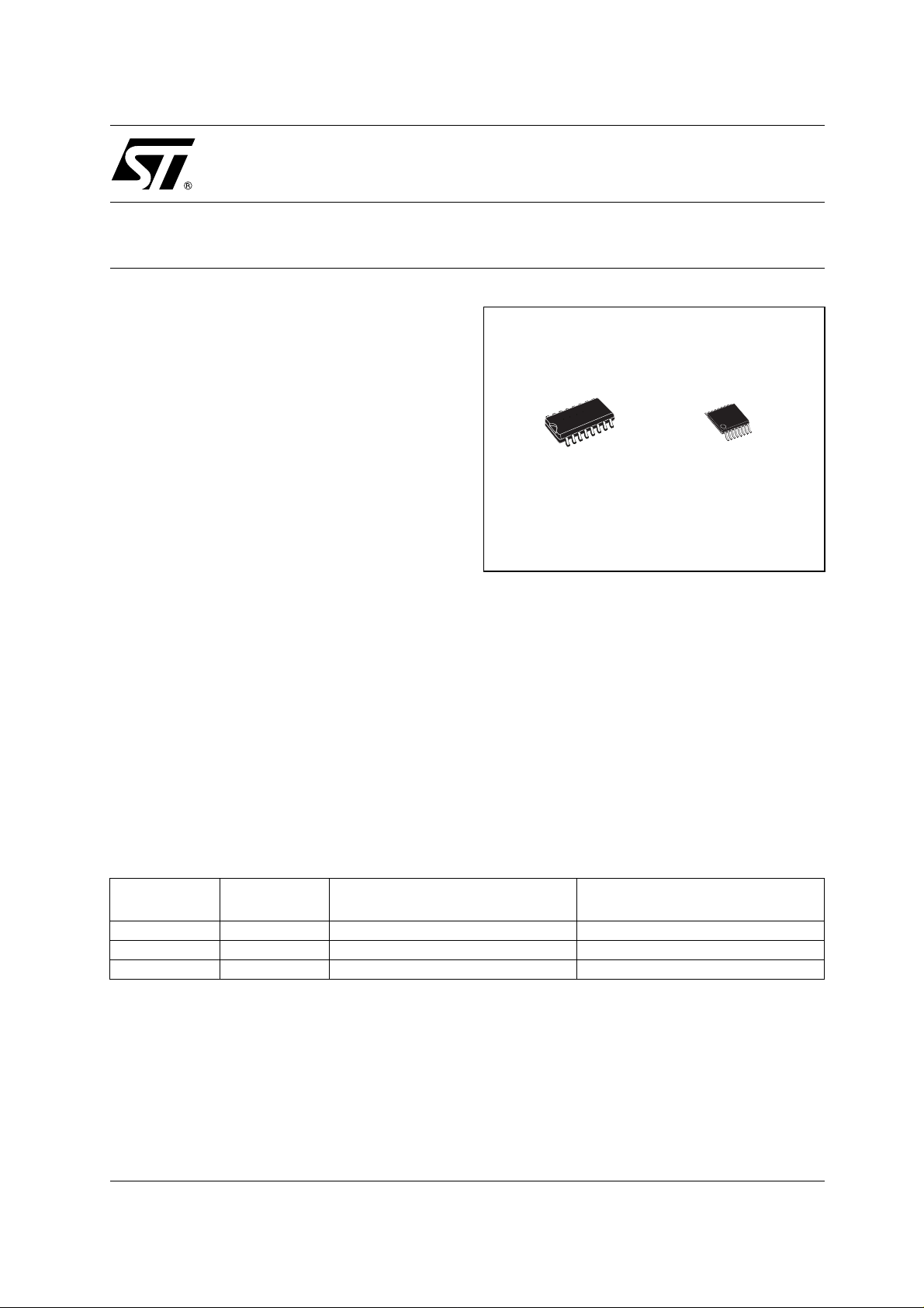
■ AVAILABLE IN SURFACE MOUNT (S OIC)
AND LOW PROFILE TSSOP PACKAGE
DESCRIPTION
The STLVDS47 is a quad CMOS flow-through
differential line driver designed for applications
requiring ultra low power dissipation and high data
rate. The device is designed to support data rates
in excess of 400Mbp s (200 MHz) utilizing Low
Voltage Differential Signaling (LVDS) techology.
The STLVDS47 accepts low voltage TTL/CMOS
input levels and translates them to low voltage
STLVDS47
SO-16 TSSOP
(350 mV) differential output signals. In addition,
the driver support a TRI-STATE function that may
be used to disable the output stage, disabling the
load current, and thus dropping the device to an
ultra low idle power state of 1.3mW typical. The
STLVDS47 has a flow-through pinout f or easy
PCB layout.
The E N and EN* inputs are AN Ded together and
control the TRI-STATE output.
TheSTLVDS47andcompanionlinereceiver
(STLVDS48) provide a new alternative to high
power pseudo-ECL devices for high-speed
point-to-point interface applications.
ORDERING CODES
Type
STLVDS47BD -40 to 85 °C SO-16 (Tube) 50 parts per tube / 20 tube per box
STLVDS47BDR -40 to 85 °C SO-16 (Tape & Reel) 2500 parts per reel
STLVDS47BTR -40 to 85 °C TSSOP-16 (Tape & Reel) 2500 parts per reel
Temperature
Range
Package Comments
1/10December 2002
Page 2
STLVDS47
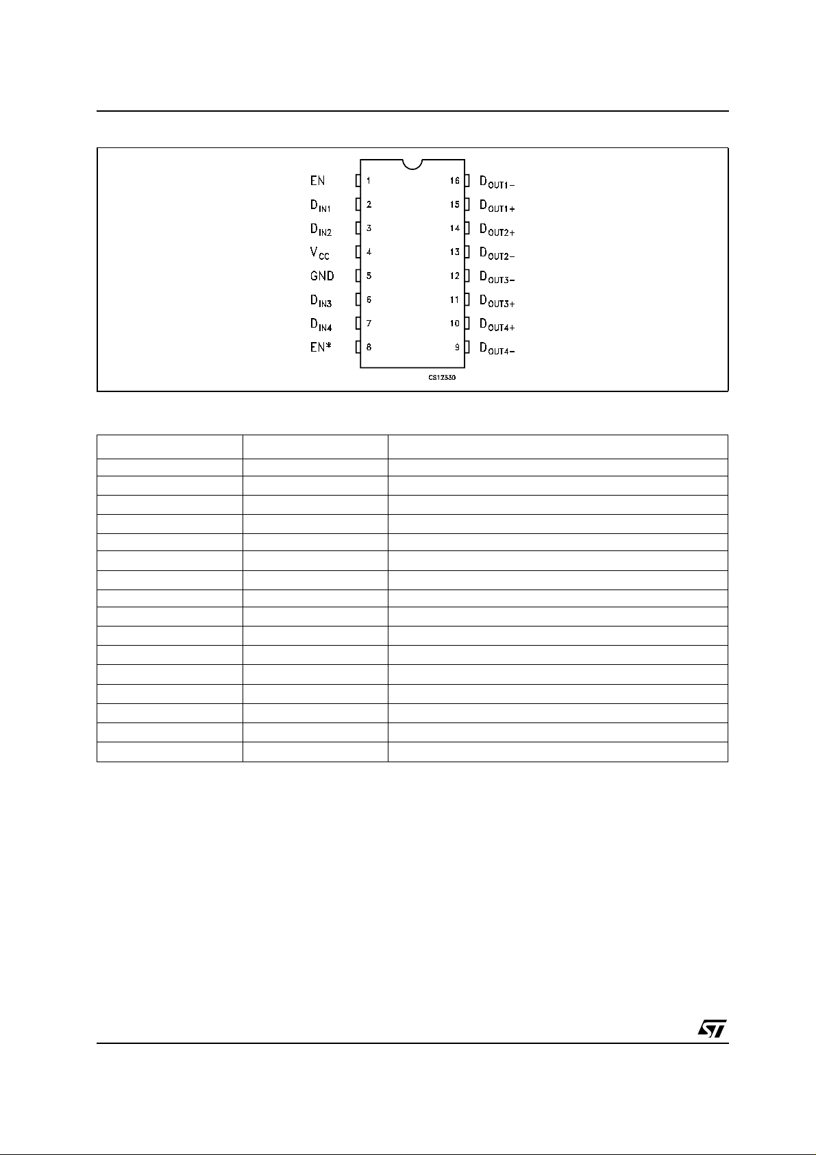
PIN CONFIGURATION
PIN DESCRIPTION
PlN N° SYMBOL NAME AND FUNCTION
1 EN Enable
2
3
4
5 GND GROUND
6
7
8 EN* Enable (inverting)
9D
10
11
12
13
14
15
16
D
D
V
D
D
OUT4-
D
OUT4+
D
OUT3+
D
OUT3-
D
OUT2-
D
OUT2+
D
OUT1+
D
OUT1-
IN1
IN2
CC
IN3
IN4
First Driver Input
Second Driver Input
Supply Voltage
Third Driver Input
Fourth Driver Input
Fourth Driver Inverting Output
Fourth Driver non-Inverting Output
Third Driver non-Inverting Output
Third Driver Inverting Output
Second Driver Inverting Output
Second Driver non-Inverting Output
First Driver non-Inverting Output
First Driver Inverting Output
2/10
Page 3
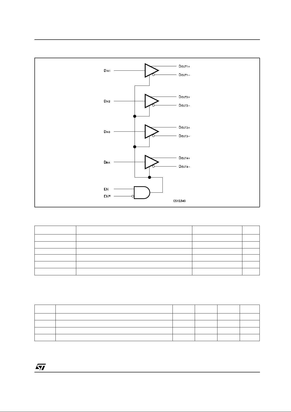
FUNCTIONAL DIAGRAM
STLVDS47
ABSOLUTE MAXIMUM RATINGS
Symbol Parameter Value Unit
V
CC
D
IN
Supply Voltage
Input Voltage
-0.3 to 4 V
-0.3 to 6 V
EN, EN* Enable Input Voltage -0.3 to 6 V
D
OUT+,DOUT-
I
SCTOUT
T
stg
Absolute Maximum Ratings are those values beyond which damage to the device may occur. Functional operation under these condition is
not implied.
Output Voltage
Short Circuit Duration
Storage Temperature Range
-0.3 to 3.9 V
Continuous
-65 to +150 °C
RECOMMENDED OPERATIN G CONDITIONS
Symbol Parameter Min TYP Max Unit
V
V
V
Supply Voltage
CC
High-Level Input Voltage
IH
Low-Level Input Voltage
IL
Operating Free-Air Temperature
T
A
3 3.3 3.6 V
2V
0.8 V
-40 85 °C
3/10
Page 4

STLVDS47
ELECTRICAL CHARACTERISTICS (Typical values are at TA= 25°C, VCC= 3.3V ± 10% ,
T
= -40 to 85 °C, unless otherwise specified). (Note 1, 2)
A
Symbol Parameter Test Conditions
Min. Typ. Max.
V
∆V
Differential Output Voltage RL= 100 Ω 247 350 454 mV
OD1
Change in Magnitude of V
OD1
OD1
for
-35 35 |mV|
Complementary Output States
V
∆V
Offset Voltage 1.125 1.2 1.375 V
OC
Change in Magnitude of VOSfor
OC
-25 25 |mV|
Complementary Output States
Input High Current VIN=2V 20 µA
I
IH
Input Low Current VIN= 0.8V 10 µA
I
IL
Output Short Circuit Current
I
OS
(Note 3)
I
I
I
I
NOTE 1: Current into device pins is defined as positive. Current out of device pins as negative. All voltage are reference to ground except:
V
OD1
NOTE 2: The STLVDS47 is a current mode device and only functions within datasheet specifications when a resostive load is applied to the
driver outputs typical range is (90
NOTE 3: Output short circuit current (IOS) is specified as magnitude only, minus sign indicates direction only.
Differential Output Short Circuit
OSD
(Note 3)
Power-off Leakage V
OFF
I
Output TRI-STATE Current EN = 0.8V and EN* = 2V
OZ
Loaded Supply Current Drivers
CCL
Enabled
No Load Supply Current Drivers
CCZ
Disabled
and ∆V
OD1
.
Ω to 110 Ω).
ENABLED, DIN=VCC,
D
=0VorDIN=GND,
OUT+
D
=0V
OUT-
ENABLED, VOD= 0V 3 10 mA
= 0V or 3.6V,
OUT
= 0V or Open
V
CC
=0VorV
V
OUT
CC
RL= 100 Ω All Channels,
D
IN =VCC
D
IN =VCC
EN = GND, EN* = V
or GND (all inputs)
or GND,
CC
Value
Unit
610mA
±1 µA
±1 µA
18 26 mA
0.4 1 mA
4/10
Page 5

SWITCHING CHARACTERISTICS (Typical values are at TA= 25°C, VCC= 3.3V ± 10% ,
T
= -40 to 85 °C, unless otherwise specified). (Note 1, 2)
A
Symbol Parameter Test Conditions
Min. Typ. Max.
t
t
t
SK(p)
t
SK(o)
t
SK(pp)
t
t
t
t
f
MAX
NOTE 1: CLincludes probe and jig capacitance.
NOTE2: t
together.
NOTE 3:t
vices operate with same supply voltage, at the same temperature, and have identical packages and test circuits.
Propagation Delay Time Low-to-
PLH
High-Level output
Propagation Delay Time High-to-
PHL
Low-Level output
Differential Output signal rise time 0.5 1 ns
t
r
Differential Output signal fall time 0.5 1 ns
t
f
Pulse Skew (|t
PHL-tPLH
|) 100 300 ps
Channel-to-Channel Output Skew
(Note 1)
Part-to-Part Skew (Note 2) 1 ns
Propagation Delay Time, high-
PZH
impedance-to-high-level output
Propagation Delay Time, high-
PZL
impedance-to-low-level output
Propagation Delay Time, high-
PHZ
level-to-high-impedance output
Propagation Delay Time, low-
PLZ
level-to-high-impedance output
Maximum Operating Frequency 250 MHz
is the magnitude of the time difference between the t
SK(o)
is the magnitude of the difference in propagation delay times between any specified terminals of two devices when both de-
SK(pp)
RL= 100 Ω,CL= 5 pF 1.6 1.8 2.7 ns
1.6 1.8 2.7 ns
ort
PLH
of alldrivers of asingle device with alloftheirinputs connected
PHL
Value
100 300 ps
5.4 10 ns
7.4 12 ns
3.5 6 ns
3.9 6 ns
STLVDS47
Unit
5/10
Page 6

STLVDS47
SO-16 MECHANICAL DATA
DIM.
A 1.75 0.068
a1 0.1 0.2 0.004 0.008
a2 1.65 0.064
b 0.35 0.46 0.013 0.018
b1 0.19 0.25 0.007 0.010
C 0.5 0.019
c1 45˚ (typ.)
D 9.8 10 0.385 0.393
E 5.8 6.2 0.228 0.244
e 1.27 0.050
e3 8.89 0.350
F 3.8 4.0 0.149 0. 157
G 4.6 5.3 0. 181 0.208
L 0.5 1.27 0.019 0.050
M 0.62 0.024
S8 ˚ (max.)
MIN. TYP MAX. MIN. TYP. MAX.
mm. inch
6/10
PO13H
Page 7

STLVDS47
TSSOP16 MECHANICAL DATA
mm. inch
DIM.
MIN. TYP MAX. MIN. TYP. MAX.
A 1.2 0.047
A1 0.05 0.15 0.002 0.004 0.006
A2 0.8 1 1.05 0.031 0.039 0.041
b 0.19 0.30 0.007 0.012
c 0.09 0.20 0.004 0.0079
D 4.9 5 5.1 0.193 0.197 0.201
E 6.2 6.4 6.6 0.244 0.252 0.260
E1 4.3 4.4 4.48 0.169 0.173 0.176
e 0.65 BSC 0.0256 BSC
K0˚ 8˚0˚ 8˚
L 0.45 0.60 0.75 0.018 0.024 0.030
A2
A
A1
b
e
c
K
L
E
D
E1
PIN 1 IDENTIFICATION
1
0080338D
7/10
Page 8

STLVDS47
Tape & Reel SO-16 MECHANICAL DATA
mm. inch
DIM.
MIN. TYP MAX. MIN. TYP. MAX.
A 330 12.992
C 12.8 13.2 0.504 0.519
D 20.2 0.795
N 60 2.362
T 22.4 0.882
Ao 6.45 6.65 0.254 0.262
Bo 10.3 10.5 0.406 0.414
Ko 2.1 2.3 0.082 0.090
Po 3.9 4.1 0.153 0.161
P 7.9 8.1 0.311 0.319
8/10
Page 9

STLVDS47
Tape & Reel TSSOP16 MECHANICAL DATA
mm. inch
DIM.
MIN. TYP MAX. MIN. TYP. MAX.
A 330 12.992
C 12.8 13.2 0.504 0.519
D 20.2 0.795
N 60 2.362
T 22.4 0.882
Ao 6.7 6.9 0.264 0.272
Bo 5.3 5.5 0.209 0.217
Ko 1.6 1.8 0.063 0.071
Po 3.9 4.1 0.153 0.161
P 7.9 8.1 0.311 0.319
9/10
Page 10

STLVDS47
Information furnished is believed to be accurate and reliable. However, STMicroelectronics assumes no responsibilit y for t he
consequences of use of such informatio n nor for any infringement of paten ts or o ther rig hts of t hird part ies which ma y result from
its use. No license is granted by implication or otherwise under any patent or patent rights of STMicroelectronics. Specifications
mentioned in this publication are subject to change without notice. This publication supersedes and replaces all information
previousl y suppl ied. STM icroel ectronics produc ts are not auth orized for use as c ritica l compone nts in l ife s upport dev ices or
systems without express written approval of STMicroelectronics.
Australia - Brazil - Canada - China - Finland - France - Germany - Hong Kong - India - Israel - Italy - Japan - Malaysia - Malta - Morocco
© The ST logo is a registered trademark of STMicroelectronics
© 2002 STMicroelectronics - Printed in Italy - All Rights Reserved
STMicroelectronics GROUP OF COMPANIES
Singapore - Spain - Sweden - Switzerland - United Kingdom - United States.
© http://www.st.com
10/10
 Loading...