

Datasheet STLVDS3487BDR, STLVDS3487BTR, STLVDS3487BD, STLVDS31BDR, STLVDS31BTR Datasheet (SGS Thomson Microelectronics)
...Page 1
1/13May 2003
■ MEETS OR EXCEEDS THE
REQUIREMENTS OF ANSI TIA/EIA-644
STANDARD
■ LOW VOLTAGE DIFFERENTIAL SIGNALING
WITH TYPICAL OUTPUT VOLTAGE OF
350mV AND A 100Ω LOAD
■ TYPICAL OUTPUT VOLTAGE RISE AND
FALL TIMES OF 750ps (400Mbps)
■ TYPICAL PROPAGATION DELAY TIMES OF
1.7ns
■ OPERATES FROM A SINGLE 3.3V SUPPLY
■ POWER DISSIPATION 25mW TYPICAL PER
DRIVER AT 200MHz
■ DRIVER AT HIGH IMPEDANCE WHEN
DISABLEDORWITHV
CC
=0V
■ PIN COMPATIBLE WITH THE AM26LS31,
SN65LVD31
■ LOW VOLTAGE TTL (LVTTL) LOGIC INPUT
LEVELS
DESCRIPTION
The STLVDS31 is a quad differential line drivers
that implements the electrical characteristics of
low voltage differential signaling (LVDS). This
signaling technique lowers the output voltage
levels of 5V differential standard levels (such as
TIA/EIA-422B) to reduce the power, increase the
switching speeds and allows operations with a
3.3V supply rail. Any of the four current mode
drivers will deliver a minimum differential output
voltage magnitude of 247m V into a 100Ω load
when enabled.
The intended application of this device and
signalling technique is for point-to-point baseband
data transmission over controlled impedance
media approximat ely 100Ω. The transmission
media may be printed circuit board traces,
backplanes or cables. The ultimate rate and
distance of data transfer is dependent upon the
attenuation characte ristics of the media and noise
coupling to the environment.
The STLVDS31 is characterized for op eration
from -40°C to 85°C.
ORDERING CODES
Type
Temperature
Range
Package Comments
STLVDS31BD -40 to 85 °C SO-16 (Tube) 50parts per tube / 20tube per box
STLVDS31BDR -40 to 85 °C SO-16 (Tape & Reel) 2500 parts per reel
STLVDS31BTR -40 to 85 °C TSSOP16 (Tape & Reel) 2500 parts per reel
STLVDS31
HIGH SPEED
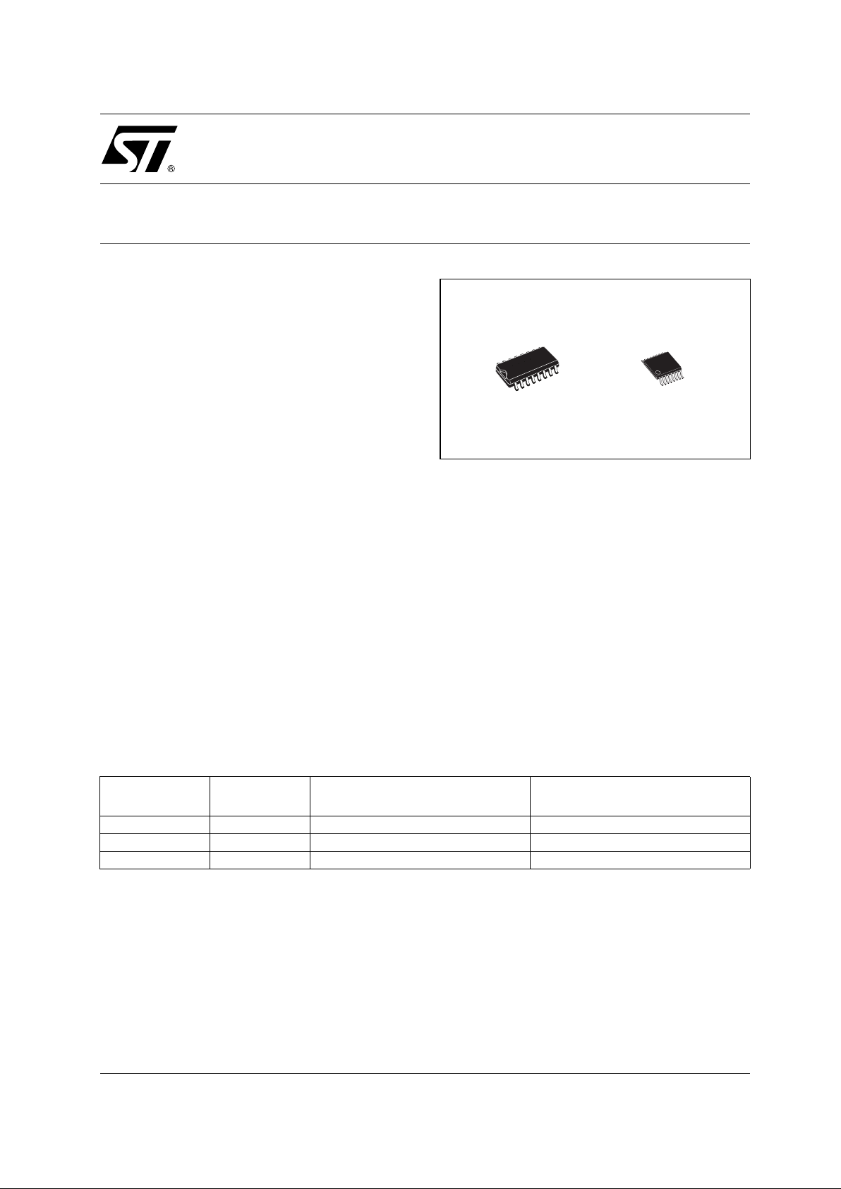
DIFFERENTIAL LINE DRIVERS
SOP TSSOP
Page 2
STLVDS31
2/13
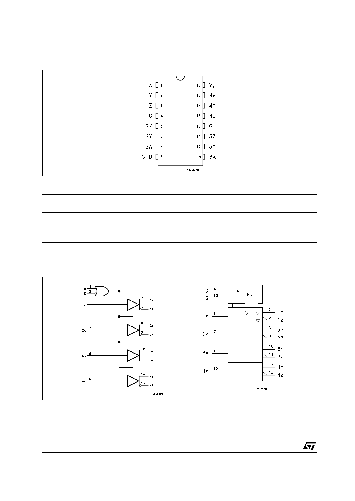
PIN CONFIGURATION
PIN DESCRIPTION
LOGIC DIAGRAM AND LOGIC SYMBOL
PlN N° SYMBOL NAME AND FUNCTION
1, 7, 9, 15 1A to 4A Driver Inputs
2, 6, 10, 14 1Y to 4Y Driver Outputs
3, 5, 11, 13 1Z to 4Z Driver Outputs
4 G Enable
12 G
Enable
8 GND Ground
16
V
CC
Supply Voltage
Page 3
STLVDS31
3/13
TRUTH TABLE
L=Low level, H=High Level, X=Don’t care, Z= High Impedance
ABSOLUTE MAXIMUM RATINGS
Absolute Maximum Ratings are those values beyond which damage to the device may occur. Functional operation under these condition is
not implied.
Note 1: All voltages except differential I/O bus voltage, are with respect to the network ground terminal.
RECOMMENDED OPERATING CONDITIONS
INPUT ENABLES OUTPUTS
AGG
YZ
HHXHL
LHXLH
HXLHL
LXLLH
XLHZZ
OPEN H X L H
OPEN X L L H
Symbol Parameter Value Unit
V
CC
Supply Voltage (Note 1)
-0.5 to 4.6 V
V
I
DC Input Voltage -0.5 to (VCC+ 0.5)
V
T
stg
Storage Temperature Range
-65 to +150 °C
Symbol Parameter Min. Typ. Max. Unit
V
CC
Supply Voltage 3.0 3.3 3.6 V
V
IH
HIGH Level Input Voltage 2.0 V
V
ILI
LOW Level Input Voltage 0.8 V
T
A
Operating Temperature Range
-40
85
°C
Page 4
STLVDS31
4/13
ELECTRICAL CHARACTERISTICS (Over recommended operating conditions unless otherwise noted.
All typical values are at T
A
= 25°C, and VCC=3.3V)
Symbol Parameter Test Conditions Min. Typ. Max. Unit
V
OD
Differential Output Voltage RL= 100Ω Fig. 2 247 350 454 mV
∆V
OD
Change in Differential
Output Voltage Between
Logic State
-50 50 mV
∆V
OC(SS)
Change in Steady-state
Common Mode Output
Voltage Between Logic
State
Fig. 3 1.125 1.2 1.375 V
V
OC(SS)
Steady-state Common
Mode Output Voltage
Fig. 3 -50 50 mV
V
OC(PP)
Peak to Peak Common
mode Output Voltage
80 150 mV
I
CC
Supply Current VIN= 0.8V or 2V, Enabled, No Load 11.5 20 mA
V
IN
= 0.8V or 2V, Enabled, RL=100Ω 25 35 mA
V
IN
= 0 or VCC, Disabled 0.3 1 mA
I
IH
High Level Input Current VIH=2V 4 20 µA
I
IL
Low Level Input Current VIL= 0.8V 0.6 10 µA
I
SC
Short Circuit Output Current V
O(Y)
or V
O(Z)
= 0V 6.1 -24 mA
V
OD
=0 ± 12 mA
I
OZ
High Impedance Output
Current
VO= 0 or 2.4V ± 1 µA
I
OFF
Power OFF Output Current VCC=0 VO= 2.4V ± 1 µA
C
IN
Input Capacitance 3 pF
Page 5

STLVDS31
5/13
SWITCHING CHARACTERISTICS (Unless otherwise noted. Typical values are referred to TA=25°C
and V
CC
=3.3V)
Note 1: t
sk(O)
is themaximum delaytime differencebetween drivers on the samedevice.
Note 2: RS-232 IN to TTL-CMOS OUT (from 50% to 50%)
Figure1 : Voltage and Current Definitions
Symbol Parameter Test Conditions Min. Typ. Max. Unit
t
PLH
Propagation Delay Time,
Low to High Output
RL=100Ω CL= 10pF
Fig. 2
0.5 1.4 2 ns
t
PHL
Propagation Delay Time,
High to Low Output
1 1.7 2.5 ns
t
r
Differential Output Signal
Rise Time
0.4 0.5 0.6 ns
t
f
Differential Output Signal
Fall Time
0.4 0.5 0.6 ns
t
sk(P)
Pulse Skew (|t
THL=tTLH
|) 0.3 0.6 ns
t
sk(O)
Channel to Channel Output
Skew (note1)
0 0.3 ns
t
PZH
Propagation Delay Time,
High Impedance to High
Level Output
Fig. 4 5.4 15 ns
t
PZL
Propagation Delay Time,
High Impedance to Low
Level Output
2.5 15 ns
t
PHZ
Propagation Delay Time,
High Level to High
Impedance Output
8.1 15 ns
t
PLZ
Propagation Delay Time,
Low Level to High
Impedance Output
7.3 15 ns
Page 6

STLVDS31
6/13
Figure 2 : Test Circuit, Timing A nd Voltage Definitions For Differential Output Signal
Note A: All input pulse are supplied by a generator having the following characteristics: tror tf≤ 1ns, pulse repetition rate (PRR) = 50Mpps,
pulsewidth = 10 ± 0.2ns.
Note B: C
L
includes instrumentation and fixture capacitance within 6mm of the D.U.T.
Figure 3 : Test Circuit And Definitions For The Driver Common Mode Out put Voltage
Note A: All input pulse are supplied by a generator having the following characteristics: tror tf≤ 1ns, pulse repetition rate (PRR) = 50Mpps,
pulsewidth = 10 ± 0.2ns.
Note B: C
L
includes instrumentation and fixture capacitance within 6mm of the D.U.T
Note C: The measurement of VOC(PP) is made on test equipment with a -3dB bandwidth of at least 300MHz
Page 7

STLVDS31
7/13
Figure4 : Enable AndDisable Time Test Circuit And Waveform
Note A: All input pulse are supplied by a generator having the following characteristics: tror tf≤ 1ns, pulse repetition rate (PRR) = 0.5Mpps,
pulse width = 500 ± 10ms.
Note B: C
L
includes instrumentation and fixture capacitancewithin 6mm of theD.U.T.
Page 8

STLVDS31
8/13
TYPICAL PERFORMANCE CHARACTE RISTICS (unless otherwise specified Tj=25°C)
Figure5 : Supply Current vs Temperature
Figure6 : Supply Current vs Temperature
Figure7 : Propagation D elay Enable to Output
Figure8 : Propagation D elay Time
Figure9 : Differential Output Signal
Page 9

STLVDS31
9/13
DIM.
mm. inch
MIN. TYP MAX. MIN. TYP. MAX.
A 1.75 0.068
a1 0.1 0.2 0.004 0.008
a2 1.65 0.064
b 0.35 0.46 0.013 0.018
b1 0.19 0.25 0.007 0.010
C 0.5 0.019
c1 45˚ (typ.)
D 9.8 10 0.385 0.393
E 5.8 6.2 0.228 0.244
e 1.27 0.050
e3 8.89 0.350
F 3.8 4.0 0.149 0.157
G 4.6 5.3 0.181 0.208
L 0.5 1. 27 0.019 0.050
M 0.62 0.024
S8 ˚ (max.)
SO-16 MECHANICAL DATA
PO13H
Page 10

STLVDS31
10/13
DIM.
mm. inch
MIN. TYP MAX. MIN. TYP. MAX.
A 1.2 0.047
A1 0.05 0.15 0.002 0.004 0.006
A2 0.8 1 1.05 0.031 0.039 0.041
b 0.19 0.30 0.007 0.012
c 0.09 0.20 0.004 0.0079
D 4.9 5 5.1 0.193 0.197 0.201
E 6.2 6.4 6.6 0.244 0.252 0.260
E1 4.3 4.4 4.48 0.169 0.173 0.176
e 0.65 BSC 0.0256 BSC
K0˚ 8˚0˚ 8˚
L 0.45 0.60 0.75 0.018 0.024 0.030
TSSOP16 MECHANICAL DATA
c
E
b
A2
A
E1
D
1
PIN 1 IDENTIFICATION
A1
L
K
e
0080338D
Page 11

STLVDS31
11/13
DIM.
mm. inch
MIN. TYP MAX. MIN. TYP. MAX.
A 330 12.992
C 12.8 13.2 0.504 0.519
D 20.2 0.795
N 60 2.362
T 22.4 0.882
Ao 6.45 6.65 0.254 0.262
Bo 10.3 10.5 0.406 0.414
Ko 2.1 2.3 0.082 0.090
Po 3.9 4.1 0.153 0.161
P 7.9 8.1 0.311 0.319
Tape & Reel SO-16 MECHANICAL DATA
Page 12

STLVDS31
12/13
DIM.
mm. inch
MIN. TYP MAX. MIN. TYP. MAX.
A 330 12.992
C 12.8 13.2 0.504 0.519
D 20.2 0.795
N 60 2.362
T 22.4 0.882
Ao 6.7 6.9 0.264 0.272
Bo 5.3 5.5 0.209 0.217
Ko 1.6 1.8 0.063 0.071
Po 3.9 4.1 0.153 0.161
P 7.9 8.1 0.311 0.319
Tape & Reel TSSOP16 MECHANICAL DATA
Page 13

STLVDS31
13/13
Information furnished is believed to be accurate and reliable. However, STMicroelectronics assumes no responsibility for the
consequences of use o f suc h inf ormat ion n or f or an y infr ingeme nt of paten ts or oth er ri gh ts of third part ies whic h may resul t f rom
its use. No license is granted by implication or otherwise under any patent or patent rights of STMicroelectronics. Specifications
mentioned in this publication are subject to change without notice. This publication supersedes and replaces all information
previously supplied. STMicroelectronics products are not authorized for use as critical components in life support devices or
systems without express written approval of STMicroelectronics.
© The ST logo is a registered trademark of STMicroelectronics
© 2003 STMicroelectronics - Printed in Italy - All Rights Reserved
STMicroelectronics GROUP OF COMPANIES
Australia - Brazil - Canada - China - Finland - France - Germany - Hong Kong - India - Israel - Italy - Japan - Malaysia - Malta - Morocco
Singapore - Spain - Sweden - Switzerland - United Kingdom - United States.
© http://www.st.com
 Loading...