

Page 1
4-PORT LVDS AND 4-PORT TTL-TO LVDS
■ RECEIVER AND DRIVERS MEET OR
EXCEED THE REQUIREMENTS OF ANSI
EIA/TIA-644 STANDARD: RECEIVERS
LOW-VOLTAGE TTL (LVTTL) LEVELS
DESIGNED FOR SIGNALING RATES UP TO
630Mbps
■ OPERATES FROM A SINGLE 3.3V SUPPLY
■ LOW VOLTAGE DIFFERENTIAL SIGNALING
WITH TYPICAL OUTPUT VOLTAGE OF
350mV AND A 100Ω LOAD
■ PROPAGATION DELAY TIME: 2.2ns (TYP)
■ ELECTRICALLY COMPATIBLE WITH LVDS,
PECL, LVPECL, LVTTL, LVCOMOS, GTL,
BTL, CTT, S STL, OR HSTL OUTPUTS W ITH
EXTERNAL NETWORK
■ BUS TERMINAL ESD (HBM) EXCEEDS 7KV
■ SO AND TSSOP PACKAGING
DESCRIPTION
The STL VDS 105 is a differential line receiver and
a LVTTL input connected to four differential line
drivers that implement the electrical
characteristics of low voltagedifferential signaling,
for point to point baseband data transmission over
controlled impedance media of approximately
100Ω. The trans mission media can be
printed-circuit board traces, backplanes, or cable.
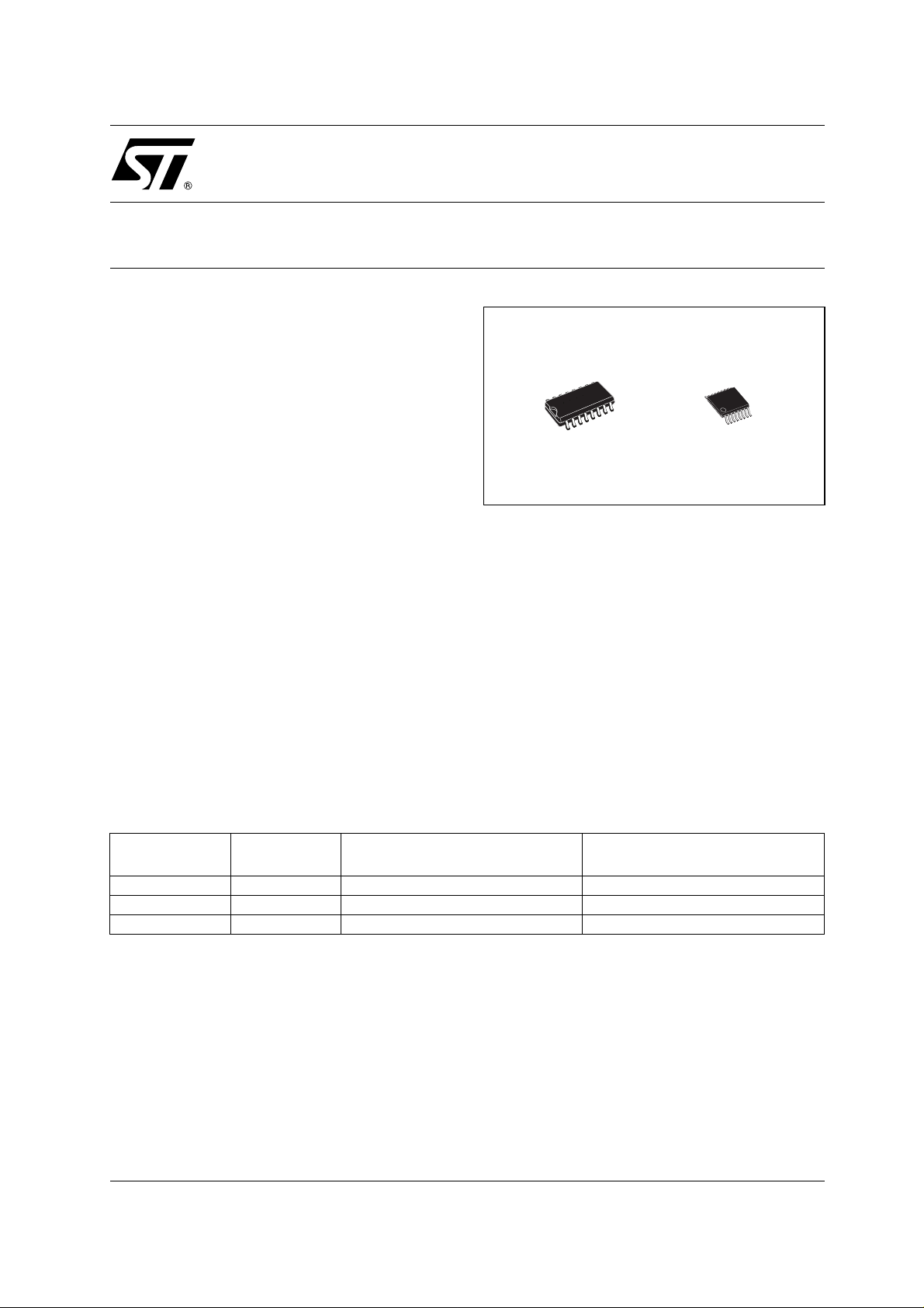
STLVDS105
REPEATERS
SOP TSSOP
LVDS, as specified in EIA/TIA-644 is a data
signaling technique that offers low-power, low
noise coupling, and switching s peed to transmit
data at a speed up to 630Mbps at relatively long
distances.
The drivers integrated into t he same substra te,
along with the low pulse skew of balanced
signaling, allow extremely precise timing
alignment of the signals repeated from the input.
The device allows extremely precise timing
alignment of the signal rep eated from the input.
This is particularly advantageous in distribution or
expansion of s ignals such as clock or serial data
stream.
ORDERING CODES
Type
STLVDS105BD -40 to 85 °C SO-16 (Tube) 50parts per tube / 20tube per box
STLVDS105BDR -40to 85 °C SO-16 (Tape & Reel) 2500 parts per reel
STLVDS105BTR -40 to 85 °C TSSOP16 (Tape & Reel) 2500 parts per reel
Temperature
Range
Package Comments
1/8May 2003
Page 2
STLVDS105
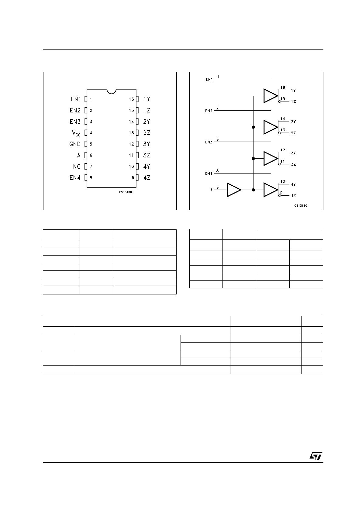
PIN CONFIGURATION
PIN DESCRIPTION
PlN N° SYMBOL NAME AND FUNCTION
1, 2, 3, 8 EN1 to EN4 Enable Driver Inputs
6 A Receiver Input
7 NC Not Connected
9, 11, 13, 15 1Z to 4Z Driver Inputs
10, 12, 14, 16 1X to 4X Driver Inputs
5 GND Ground
4
V
CC
Supply Voltage
FUNCTIONAL DIAGRAM
FUNCTIONAL TABLE
INPUT ENABLES OUTPUTS
A #EN #Y #Z
LHLH
HHHL
Open H L H
XLZZ
XXZZ
L=Low level, H=High Level, Z= High Impedance
ABSOLUTE MAXIMUM RATINGS
Symbol Parameter Value Unit
V
V
ESD ESD Protection Voltage (HBM) Y, Z, to GND 7 KV
T
Absolute Maximum Ratings are those values beyond which damage to the device may occur. Functional operation under these condition is
not implied.
Note 1: All voltages except differential I/O bus voltage, are with respect to the network ground terminal.
2/8
Supply Voltage (Note 1)
CC
Voltage Range Enable Inputs -0.5 to 6 V
R
-0.5 to 4 V
A, Y or Z -0.5 to 4 V
All Pins 2 KV
Storage Temperature Range
stg
-65 to +150 °C
Page 3
STLVDS105
RECOMMENDED OPERATING CONDITIONS
Symbol Parameter Min. Typ. Max. Unit
V
V
V
|V
V
T
Supply Voltage 3.0 3.3 3.6 V
CC
HIGH Level Input Voltage 2.0 V
IH
LOW Level Input Voltage 0.8 V
IL
| Magnitude Of Differential Input Voltage 0.1 3.6 V
ID
Common Mode Input Voltage |VID|/2 24-|VID|/2 V
IC
-0.8
V
CC
Operating Temperature Range
A
-40
85
°C
ELECTRICAL CHARACTERISTICS (T
operating conditions unless otherwise noted. All typical values are at T
= -40 to 85°C, and VCC= 3.3V ±10% over recommended
A
=25°C)
A
Symbol Parameter Test Conditions Min. Typ. Max. Unit
| Differential Output Voltage
|V
OD
Magnitude
∆|V
| Change in Differential
OD
Output Voltage Magnitude
RL= 100Ω VID= ±100mV 247 340 454 mV
-50 50 mV
Between Logic State
∆V
OC(SS)
Change in Steady-state
Common Mode Output
-50 50 mV
Voltage Between Logic
State
V
OC(SS)
V
OC(PP)
I
CC
Steady-state Common
Mode Output Voltage
Peak to Paek Common
mode Output Voltage
Supply Current Enabled, RL=100Ω 18 28 mA
1.125 1.2 1.375 V
25 150 mV
Disabled 0.3 1 mA
I
I
I
OC
I
OZ
I
O(OFF)
C
C
High Level Input Current VIH=2V 7 20 µA
IH
Low Level Input Current VIL= 0.8V 3 10 µA
IL
Short Circuit Output Current V
High Impedance Output
or V
O(Y)
=0 ± 10 mA
V
OD
=0V ± 10 mA
O(Z)
VO= 0 or 2.4V ± 1 µA
Current
Power OFF Output Current VCC= 1.5V VO= 2.4V 0.3 ± 1 µA
Input Capacitance (A or B
IN
Inputs)
Output Capacitance (Y or Z
O
Outputs)
= 0.4 sin (4e
V
I
= 0.4 sin (4e
V
I
6πt
)+0.5V
6πt
)+0.5V, Disabled
5pF
9.4 pF
3/8
Page 4

STLVDS105
SWITCHING CHA RACTERISTICS (TA= -40 to 85°C, and VCC= 3.3V unless otherwise noted. All typical
values are at T
Symbol Parameter Test Conditions Min. Typ. Max. Unit
t
Propagation Delay Time,
PLH
Low to High Output
t
Propagation Delay Time,
PHL
High to Low Output
Differential Output Signal
t
r
Rise Time
Differential Output Signal
t
f
Fall Time
t
t
t
Note 1: t
Note2: t
operate with the same supply voltages, at the same temperature, and have identical packages and test circuit.
Pulse Skew (|t
sk(P)
Channel-to-channel Output
sk(O)
Skew (note1)
Part to part Skew (note2) 1.5 ns
sk(pp)
Propagation Delay Time,
t
PZH
High Impedance to High
Level Output
Propagation Delay Time,
t
PZL
High Impedance to Low
Level Output
Propagation Delay Time,
t
PHZ
High Level to High
Impedance Output
Propagation Delay Time,
t
PLZ
Low Level to High
Impedance Output
sk(O)
sk(pp)
= 25°C)
A
RL= 100Ω CL= 10pF 1.7 2.2 3 ns
1.7 2.2 3 ns
0.3 0.7 1.2 ns
0.3 0.7 1.2 ns
THL-tTLH
|) 50 200 ps
30 100 ps
515ns
515ns
415ns
515ns
isthetimedifferencebetweenthet
is the magnitudeofthedifference inpropagation delay times between any specified terminals oftwodevices when both devices
PLH
or t
of all drivers of a single device with all their inputs connected together.
PHL
4/8
Page 5

TYPICAL PERFORMANCE CHARACTERISTICS (unless otherwise specified Tj= 25°C)
Figure 1 : Output Current vs Output High Voltage
Figure 3 : High to Low Propagation Delay Time
STLVDS105
Figure 2 : Output Current vs Output Low Voltage
Figure 4 : Low to High Propagation Delay Time
5/8
Page 6

STLVDS105
SO-16 MECHANICAL DATA
DIM.
A 1.75 0.068
a1 0.1 0.2 0.004 0.008
a2 1.65 0.064
b 0.35 0.46 0.013 0.018
b1 0.19 0.25 0.007 0.010
C 0.5 0.019
c1 45˚ (typ.)
D 9.8 10 0.385 0.393
E 5.8 6.2 0.228 0.244
e 1.27 0.050
e3 8.89 0.350
F 3.8 4.0 0.149 0.157
G 4.6 5.3 0.181 0.208
L 0.5 1. 27 0.019 0.050
M 0.62 0.024
S8 ˚ (max.)
MIN. TYP MAX. MIN. TYP. MAX.
mm. inch
6/8
PO13H
Page 7

STLVDS105
TSSOP16 MECHANICAL DATA
mm. inch
DIM.
MIN. TYP MAX. MIN. TYP. MAX.
A 1.2 0.047
A1 0.05 0.15 0.002 0.004 0.006
A2 0.8 1 1.05 0.031 0.039 0.041
b 0.19 0.30 0.007 0.012
c 0.09 0.20 0.004 0.0079
D 4.9 5 5.1 0.193 0.197 0.201
E 6.2 6.4 6.6 0.244 0.252 0.260
E1 4.3 4.4 4.48 0.169 0.173 0.176
e 0.65 BSC 0.0256 BSC
K0˚ 8˚0˚ 8˚
L 0.45 0.60 0.75 0.018 0.024 0.030
A2
A
A1
b
e
c
K
L
E
D
E1
PIN 1 IDENTIFICATION
1
0080338D
7/8
Page 8

STLVDS105
Information furnished is believed to be accurate and reliable. However, STMicroelectronics assumes no responsibility for the
consequences of use o f suc h inf ormat ion n or f or an y infr ingeme nt of paten ts or oth er ri gh ts of third part ies whic h may resul t f rom
its use. No license is granted by implication or otherwise under any patent or patent rights of STMicroelectronics. Specifications
mentioned in this publication are subject to change without notice. This publication supersedes and replaces all information
previously supplied. STMicroelectronics products are not authorized for use as critical components in life support devices or
systems without express written approval of STMicroelectronics.
Australia - Brazil - Canada - China - Finland - France - Germany - Hong Kong - India - Israel - Italy - Japan - Malaysia - Malta - Morocco
© The ST logo is a registered trademark of STMicroelectronics
© 2003 STMicroelectronics - Printed in Italy - All Rights Reserved
STMicroelectronics GROUP OF COMPANIES
Singapore - Spain - Sweden - Switzerland - United Kingdom - United States.
© http://www.st.com
8/8
 Loading...