

Page 1
HIGH SPEED DIFFERENTIAL LINE
■ MEETS OR EXCEED THE REQUIREMENTS
OF ANSI EIA/TIA-644-1995 STANDARD
■ SIGNALING RATESUP TO 400Mbit/s
■ BUS TERMINAL ESD EXCEEDS 6KV
■ OPERATES FROM A SINGLE 3.3V SUPPLY
■ LOW-VOLTAGE DIFFERENTIAL SIGNALING
WITH TYPICAL OUTPUT VOLTAGE OF
350mV AND A 100Ω LOAD
■ PROPAGATIONDELAY TIMES:
DRIVER: 2ns (TYP)
RECEIVER: 3ns (TYP)
■ POWER DISSIPATION AT 200MHz:
DRIVER: 25mW (TYP)
RECEIVER: 60mW (TYP)
■ LVTTL INPUT LEVELS ARE 5V TOLERANT
■ RECEIVER HAS OPEN-CIRUIT FAIL-SAFE
DESCRIPTION
The STLVDS051 is differential line drivers and
receivers that use low-voltage differential
signaling (LVDS) to achieve signal ing rate as high
as 400Mbps.
The EIA/TIA-644 standard compliant electrical
interface provides a minimum differential output
voltage magnitude of 247 mV into a 100 Ω load
and receipt of 100 mV signals with up to 1 V of
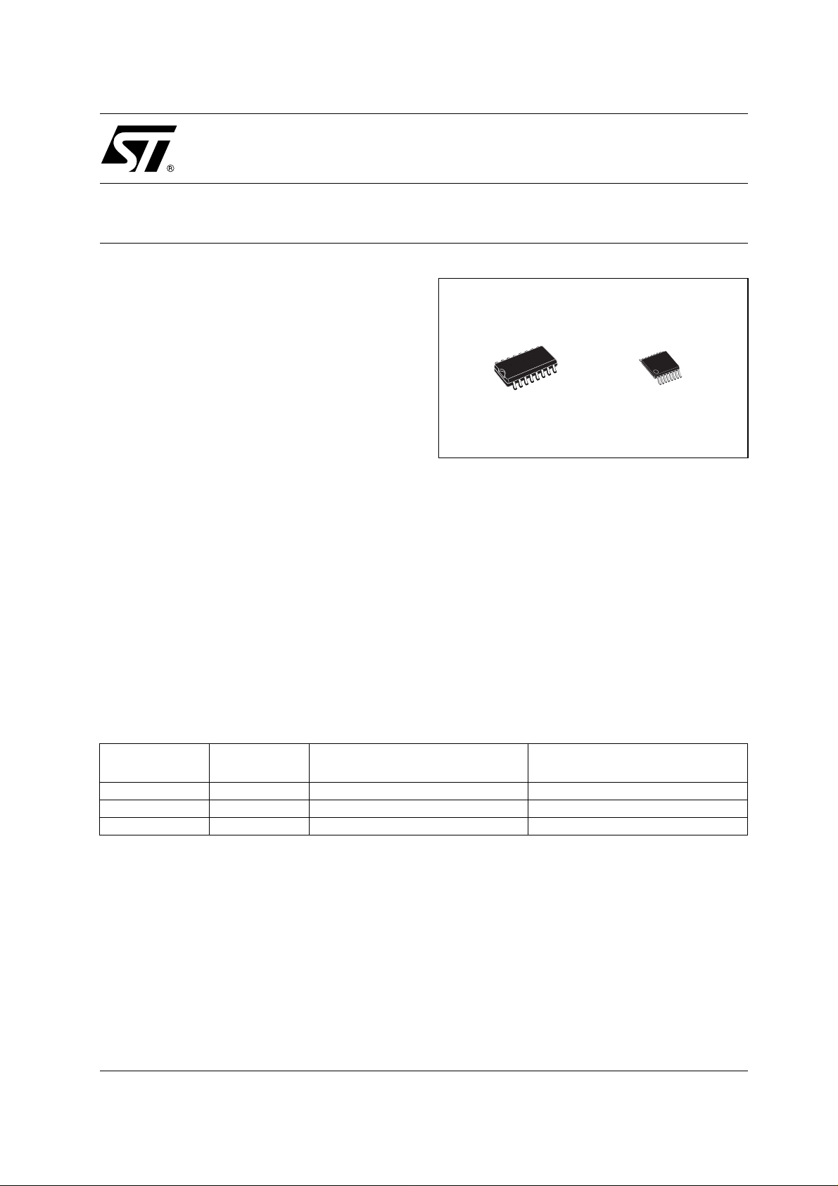
STLVDS051
DRIVERS AND R ECEIVERS
SOP TSSOP
ground potential difference between a t rans mi tter
and receiver.
The intended application of this device an
signaling technique is for point-to-point baseband
data transmission over controlled impedance
media of approximately 100 Ω characteristic
impedance.
The transmission media may be printed-circuit
board traces, backplanes, or cables. (Note: T he
ultimate rate and distance of data transfer is
dependent upon the attenuation characteristics of
the media, the noise coupling to the environme nt,
and other appl ication specific characteristics).
ORDERING CODES
Type
STLVDS051BD -40 to 85 °C SO-16 (Tube) 50 parts per tube / 20 tube per box
STLVDS051BDR -40 to 85 °C SO-16 (Tape & Reel) 2500 parts per reel
STLVDS051BTR -40 to 85 °C TSSOP16 (Tape & Reel) 2500 parts per reel
Temperature
Range
Package Comments
1/11July 2003
Page 2
STLVDS051
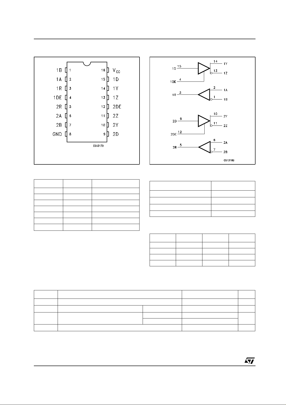
PIN CONFIGUR ATION
PIN DESCRIPTION
PlN N° SYMBOL NAME AND FUNCTION
1,2,6,7
3, 5 1R, 2R Receiver Outputs
4, 12 1DE, 2DE Driver Enable
9, 15 2D, 1D Driver Inputs
10, 11, 13, 14 2Y, 2Z, 1Y, 1Z Driver Outputs
8 GND Ground
16
1A, 1B, 2A, 2B
V
CC
Receiver Inputs
Supply Voltage
FUNCTIONAL DIAGRAM
TRUTH TABLE FOR RECEIVER
VID=VA-V
V
ID
-100mV < V
V
ID
B
≥ 100mV
< 100mV
ID
≤ −100mV
OPEN H
TRUTH TABLE FOR DRIVER
R
H
?
L
DDEY Z
LHLH
HHHL
OPEN H L H
XLZZ
L=Low level, H=High Level, X=Don’t care, Z= High Impedance
ABSOLUTE MAXIMUM RATINGS
Symbol Parameter Value Unit
V
V
ESD ESD Protection Voltage (HBM) Y, Z, A, B, and GND ± 6
T
Absolute Maximum Ratings are those values beyond which damage to the device may occur. Functional operation under these condition is
not implied.
2/11
Supply Voltage
CC
Voltage Range D, R, DE
I
Storage Temperature Range
stg
-0.5 to 4 V
-0.5 to 6 V
All Pins ± 3
-65 to +150 °C
KV
Page 3
STLVDS051
RECOMMENDED OPERATING CONDITIONS
Symbol Parameter Min. Typ. Max. Unit
V
V
V
|V
V
T
Supply Voltage 3.0 3.3 3.6 V
CC
HIGH Level Input Voltage 2.0 V
IH
LOW Level Input Voltage 0.8 V
IL
| Magnitude Of Differential Input Voltage 0.1 0.6 V
ID
Common Mode Input Voltage |VID|/2 24-|VID|/2 V
IC
-0.8
V
CC
Operating Temperature Range
A
-40
85
°C
ELECTRICAL CHARACTERISTICS (Typical values are at T
= 25°C, VCC= 3.3V ±10%, TA= -40 to 85°C
A
unless otherwise specified)
Symbol Parameter Test Conditions Min. Typ. Max. Unit
I
CC
Supply Current Drivers enabled, No Receivers load,
Driver R
=100Ω
L
Drivers Disabled, No load 4 6
DRIVER ELECTRICAL CHARACTERISTICS (Typical values are at T
T
= -40 to 85°C unless otherwise specified)
A
= 25°C, VCC=3.3V±10%,
A
Symbol Parameter Test Conditions Min. Typ. Max. Unit
| Differential Output Voltage
|V
OD
Magnitude
∆|V
| Change in Differential
OD
Output Voltage Magnitude
RL= 100Ω 247 340 454 mV
= 100Ω -50 50 mV
R
L
Between Logic States
∆V
OC(SS)
Change in Steady-state
Common Mode Output
-50 50 mV
Voltage Between Logic
States
V
OC(SS)
V
OC(PP)
Steady-state Common
Mode Output Voltage
Peak to Peak Common
mode Output Voltage
I
High Level Input Current VIH= 5V DE -0.5 -20 µA
IH
1.125 1.2 1.375 V
D220µA
I
Low Level Input Current VIL= 0.8V DE -0.5 -10 µA
IL
D110µA
I
OS
I
OZ
I
O(OFF)
C
Short Circuit Output Current V
High Impedance Output
Current
or V
O(Y)
=0 4 10 mA
V
OD
=0V 6 10 mA
O(Z)
VO= 600mV ± 1 µA
=0VorV
V
O
CC
Power OFF Output Current VCC=0V VO= 3.6V ± 1 µA
Input Capacitance 3 pF
IN
12 20 mA
50 150 mV
± 1 µA
3/11
Page 4
STLVDS051
RECEIVER ELECTRICAL CHARACTERISTICS (Typical values are at TA=25°C,VCC= 3.3V ±10%,
T
= -40 to 85°C unless otherwise specified)
A
Symbol Parameter Test Conditions Min. Typ. Max. Unit
V
ITH+
V
ITH-
V
V
I
I(OFF)
I
I
I
OZ
C
Positive-going Differential
Input Voltage Threshold
Negative-going Differential
-100 mV
Input Voltage Threshold
High Level Output Voltage IOH= -8mA 2.4 V
OH
Low Level Output Voltage IOL= 2mA 0.4 V
OL
Input Current (A or B Inputs) VI=0V -2 -11 -20 µA
I
I
= 2.4V -1 -3 µA
V
I
Power OFF Input Current
VCC=0V ±20 µA
(A or B Inputs)
High Level Input Current
IH
(Enable)
Low Level Input Current
IL
(Enable)
High Impedance Output
VIH=5V ±10 µA
VIL= 0.8V ±10 µA
VO= 0 or 5V ± 10 µA
Current
Input Capacitance 3 pF
IN
100 mV
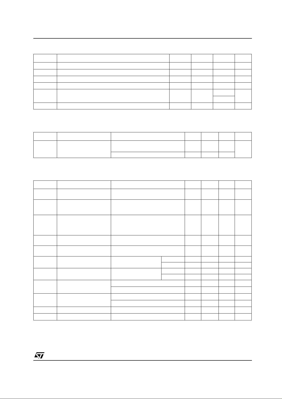
DRIVER SWITCHING CHARACTERISTICS (Typical values are at T
T
= -40 to 85°C unless otherwise specified)
A
= 25°C, VCC=3.3V±10%,
A
Symbol Parameter Test Conditions Min. Typ. Max. Unit
t
PLH
t
PHL
t
sk(P)
Propagation Delay Time,
Low to High Output
Propagation Delay Time,
High to Low Output
Differential Output Signal
t
r
Rise Time
Differential Output Signal
t
f
Fall Time
Pulse Skew (|t
THL-tTLH
RL= 100Ω CL= 10pF 2 2.7 ns
2 2.7 ns
0.4 1 ns
0.4 1 ns
|)
50 ps
(note1)
t
sk(O)
t
PZH
Channel-to-channel Output
Skew (note2)
Propagation Delay Time,
High Impedance to High
40 ps
610ns
Level Output
Propagation Delay Time,
t
PZL
High Impedance to Low
610ns
Level Output
Propagation Delay Time,
t
PHZ
High Level to High
310ns
Impedance Output
Propagation Delay Time,
t
PLZ
Low Level to High
310ns
Impedance Output
4/11
Page 5

STLVDS051
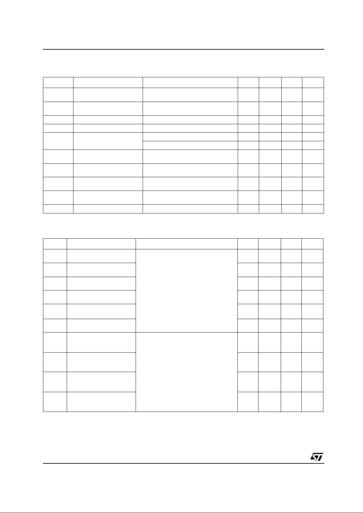
RECEIVER SWITCHING CHARACTERISTICS (Typical values are at TA=25°C,VCC= 3.3V ±10%,
T
= -40 to 85°C unless otherwise specified)
A
Symbol Parameter Test Conditions Min. Typ. Max. Unit
t
Propagation Delay Time,
PLH
Low to High Output
t
Propagation Delay Time,
PHL
High to Low Output
Differential Output Signal
t
r
Rise Time
Differential Output Signal
t
f
Fall Time
sk(P)
Pulse Skew (|t
THL-tTLH
t
(Note 1)
Propagation Delay Time,
t
PZH
High Impedance to High
Level Output
Propagation Delay Time,
t
PZL
High Impedance to Low
Level Output
Propagation Delay Time,
t
PHZ
High Level to High
Impedance Output
Propagation Delay Time,
t
PLZ
Low Level to High
Impedance Output
Note 1: t
Note 2: t
Note 3: t
supply voltages, same temperature, and have identical packages and test circuit.
is the magnitude of the time difference between the high to low and low to high propagation delay times at an output
sk(P)
is the magnitude of the time difference between the output of a single device with all their inputs connected together.
sk(O)
is the magnitude of the difference between any specified terminals of two devices when both devices operate with the same
sk(PP)
CL= 10pF 3.0 4.0 ns
3.0 4.0 ns
0.6 1 ns
0.6 1 ns
|)
0.25 ns
2.5 ns
2.5 ns
7ns
4ns
TYPICAL PERFORMANCE CHARACTE RISTICS (unless otherwise specified TJ=25°C)
Figure1 : Output Current vs Output High Voltage
for Receiver
Figure2 : Output Current vs Output Low Voltage
for Receiver
5/11
Page 6

STLVDS051
Figure3 : Output Current vs Output High Voltage
for Driver
Figure4 : Output Current vs Output Low Voltage
for Driver
Figure6 : Low to High Propagation Delay Time
for Receiver
Figure7 : High to Low Propagation Delay Time
for Driver
Figure5 : High to Low Propagation Delay Time
for Receiver
6/11
Figure8 : Low to High Propagation Delay Time
for Driver
Page 7

SO-16 MECHANICAL DATA
STLVDS051
DIM.
A 1.75 0.068
a1 0.1 0.2 0.004 0.008
a2 1.65 0.064
b 0.35 0.46 0.013 0.018
b1 0.19 0.25 0.007 0.010
C 0.5 0.019
c1 45˚ (typ.)
D 9.8 10 0.385 0.393
E 5.8 6.2 0. 228 0.244
e 1.27 0.050
e3 8.89 0.350
F 3.8 4.0 0.149 0.157
G 4.6 5.3 0.181 0.208
L 0.5 1. 27 0. 019 0.050
M 0.62 0.024
S8 ˚ (max.)
MIN. TYP MAX. MIN. TYP. MAX.
mm. inch
PO13H
7/11
Page 8

STLVDS051
TSSOP16 MECHANICAL DATA
mm. inch
DIM.
MIN. TYP MAX. MIN. TYP. MAX.
A 1.2 0.047
A1 0.05 0.15 0.002 0.004 0.006
A2 0.8 1 1.05 0.031 0.039 0.041
b 0.19 0.30 0.007 0.012
c 0.09 0.20 0.004 0.0079
D 4.9 5 5.1 0.193 0.197 0.201
E 6.2 6.4 6.6 0.244 0.252 0.260
E1 4.3 4.4 4.48 0.169 0.173 0.176
e 0.65 BSC 0.0256 BSC
K0˚ 8˚0˚ 8˚
L 0.45 0.60 0.75 0.018 0.024 0.030
A2
A
A1
b
e
c
K
L
E
D
E1
PIN 1 IDENTIFICATION
8/11
1
0080338D
Page 9

STLVDS051
Tape & Reel SO-16 MECHANICAL DATA
mm. inch
DIM.
MIN. TYP MAX. MIN. TYP. MAX.
A 330 12.992
C 12.8 13.2 0.504 0.519
D 20.2 0.795
N 60 2.362
T 22.4 0.882
Ao 6.45 6.65 0.254 0.262
Bo 10.3 10.5 0.406 0.414
Ko 2.1 2.3 0.082 0.090
Po 3.9 4.1 0.153 0.161
P 7.9 8.1 0.311 0.319
9/11
Page 10

STLVDS051
Tape & Reel TSSOP16 MECHANICAL DATA
mm. inch
DIM.
MIN. TYP MAX. MIN. TYP. MAX.
A 330 12.992
C 12.8 13.2 0.504 0.519
D 20.2 0.795
N 60 2.362
T 22.4 0.882
Ao 6.7 6.9 0.264 0.272
Bo 5.3 5.5 0.209 0.217
Ko 1.6 1.8 0.063 0.071
Po 3.9 4.1 0.153 0.161
P 7.9 8.1 0.311 0.319
10/11
Page 11

STLVDS051
Information furnished is believed to be accu rate and reliable. However, STMicroelectronics assu mes no responsibility for the
consequences of use o f suc h inf ormat ion n or f or an y infr ingeme nt of paten ts or oth er ri gh ts of third part ies whic h may resul t f rom
its use. No license is granted by implication or otherwise under any patent or patent rights of STMicroelectronics. Specifications
mentioned in this publication are subject to change without notice. This publication supersedes and replaces all information
previously supplied. STMicroelectronics products are not authorized for use as critical components in life support devices or
systems without express written approval of STMicroelectronics.
Australia - Brazil - Canada - China - Finland - France - Germany - Hong Kong - India - Israel - Italy - Japan - Malaysia - Malta - Morocco
© The ST logo is a registered trademar k of STMicroelectronics
© 2003 STMicroelectronics - Printed in Italy - All Rights Reserved
STMicroelectronics GROUP OF COMPANIES
Singapore - Spain - Sweden - Switzerland - United K ingdom - United States.
© http://www.st.com
11/11
 Loading...