

Page 1

Syntek Semiconductor Co.,Ltd.
Lcd Controller 1/ 15
STK55C321
STK55C321 SPECIFICATION
1. CHIP FEATURES :
| * Operating voltage 2.5V - 4.0V.
| * Maximum operating frequency is 3.5MHz at 4V.
| * Operating current under 1.3mA at 770KHz, 4V.
* 40 segments and 8 commons out for LCD driver.
- 1/4 duty and 244Hz frame frequency.
- 1/8 duty and 122Hz frame frequency.
* 2 bi-directional I/O port.
- 8 pins for port 1.
- 4 pins with selectable interrupt for port 2.
- 4 pins without interrupt for port 2.
* Built in 192 bytes RAM (including LCD storage area).
* Built in 10K bytes ROM.
* Selectable (system clock/16384) interrupt by NMI.
* Timer and port 2 interrupt by IRQ.
* SOUND output from CPU or two independent 16-bit counter.
* 256 sound volumes for channel 1. 8 sound volumes for channel 2.
* Code options :
- 1/3 bias or 1/4 bias for LCD driver.
- 1/4 duty or 1/8 duty for LCD driver.
- Pull-up resistors for I/O pin.
- RC or CRYSTAL oscillator.
- System clock = OSC clock or OSC clock/2.
2. APPLICATION :
* Hand-held game
Page 2

Syntek Semiconductor Co.,Ltd.
Lcd Controller 2/ 15
STK55C321
3. PIN DESCRIPTION :
Pin name I/O Function description
COM1-COM8 O Output pins for driving the common pins on the LCD panel.
SEG1-SEG40 O Output pins for driving the segment pins on the LCD panel
SOUND1 O Output pins for sound generator 1
SOUND2 O Output pins for sound generator 2
P10-P17 I/O 8 bit bi-directional pins for port 1
P20-P27 I/O 8 bit bidirectional pins for port 2
OSC1 I Oscillator input pin for chip
OSC2 O Oscillator output pin for resistor
OSC3 O Oscillator output pin for capacitor
/TEST I Test pin. Keep floating or connect to Vdd
/RES I Chip reset
V4 I Bias supply voltage pin to drive the LCD
VDD Power input
VSS Signal ground
Note: The substrate should be connected to VSS or floating.
4. ADDRESS ARRANGEMENT :
1) RAM
0000-003F for LCD output data storage area 1.
Memory address Pin for 1/8 duty Pin for 1/4 duty
0000-0004 COM1 COM1
0008-000C COM2 COM2
0010-0014 COM3 COM3
0018-001C COM4 COM8
0020-0024 COM5
0028-002C COM6
0030-0034 COM7
0038-003C COM8
0040-007F for LCD output data storage area 2.
Memory address Pin for 1/8 duty Pin for 1/4 duty
Page 3

Syntek Semiconductor Co.,Ltd.
Lcd Controller 3/ 15
STK55C321
0040-0044 COM1 COM1
0048-004C COM2 COM2
0050-0054 COM3 COM3
0058-005C COM4 COM8
0060-0064 COM5
0068-006C COM6
0070-0074 COM7
0078-007C COM8
* The LSB of low byte - SEG1.
The MSB of high byte - SEG40.
The middle bits are in the order.
The un-specified area between 0000-007F are general purpose RAM.
00C0-00FF for zero and stack page area.
* 0000-00FF are the same location with 0100-01FF.
* The data or stack can be stored in this area, but be careful not to make
conflict.
2) ROM
D800-FFFF for program area.
FFFF,FFFE - IRQ vector.
FFFD,FFFC - RES vector.
FFFB,FFFA - NMI vector.
Please note that A14 and A15 are not cared in hardware. So, following
memory areas are mapping in the same location.
0000-3FFF, 4000-7FFF, 8000-BFFF AND C000-FFFF.
3) Other
Page 4

Syntek Semiconductor Co.,Ltd.
Lcd Controller 4/ 15
STK55C321
0080 To enter stand-by mode. Write only.
* Write this address, will make CPU into stand-by mode.
* CPU will be hold with LCD state no change.
* When in stand-by mode, the NMI or IRQ will wake up the CPU. After doing
the interrupt routine, the program must access this address to enter stand-by
again.
0081 To enter power-down mode. Write only.
Bit 0 : = 0 Disable power-down mode wake up timer.(default)
= 1 Enable power-down mode wake up timer.
1 : = 1 Into power-down mode.
In power-down mode, the oscillator will be stopped & LCD will be off. After
wake up, bit 1 will be cleared to zero and programmer have to clear bit 0. If the
wake up timer is enable, an oscillator warm-up time (defined by $008B &
008C before entering power-down mode) will be added before CPU been
waked up and the IRQ1 flag will be set after wake up.
0082 Set frame frequency. Write only.
Bit 0 : = 0 System clock/8192 for 1/8 duty.(default)
System clock/4096 for 1/4 duty.
= 1 System clock/4096 for 1/8 duty.
System clock/2048 for 1/4 duty.
0083 IRQ flag register. Read & write.
* Read Bit 0 : if 1, there is timer interrupt, IRQ1.
Bit 1 : if 1, there is port 2 interrupt, IRQ2.
Write Bit 0 : if 0, clear IRQ1 flag.
Bit 1 : if 0, clear IRQ2 flag.
* When in IRQ routine, clear this register before resetting the IRQ disable flag
of the CPU. Or, it will go into IRQ loop infinitely.
* Disable port 2 interrupt function before clear IRQ1 flag.
0084 Port 1 data. Read & write.
Page 5

Syntek Semiconductor Co.,Ltd.
Lcd Controller 5/ 15
STK55C321
0085 Set port 1 bit function. Write only.
* An '0' in this register will set the corresponding pin of port 1 as an output pin.
* The default value for each bit is one. A pull-up resistor can be added to the
pin by code option. But the pull-up resistor will be disabled if the output state
is low.
0086 Port 2 data. Read & write.
0087 Set port 2 bit function. Write only.
* An '0' in this register will set the corresponding pin of port 2 as an output pin.
* The default value for each bit is one. A pull-up resistor can be added to the
pin by code option. But the pull-up resistor will be disabled if the output state
is low.
0088 Set port 2 bit interrupt function. Write only.
Bit 3-0 : Set interrupt function.
7-4 : Reserved.
* An '0' in this register will set the interrupt function of the corresponding pin of
port 2 to be enable. That is, an interrupt will be generated if a low level is
detected in the pin.
* The default value for each bit is one.
0089 Set low byte of sound generator 1 frequency divider. Write only.
008A Set high byte of sound generator 1 frequency divider. Write only.
* Program sequence should be low byte first then high byte.
* Output frequency = system clock/[($008A)x256+($0089)+1]/2
008B Timer data. Read & write.
* Before writing $008B, the program should select timer clock ($008C) first.
* After $008B been written, the timer will start to count down. When timer
Page 6

Syntek Semiconductor Co.,Ltd.
Lcd Controller 6/ 15
STK55C321
counts to zero, IRQ1 will happen.
* The time elapse = [($008B)+1]/timer clock
008C Timer clock select for different interrupt time range. Write only. (default
unknown)
Bit 2-0 : = 000 System clock/2
= 001 System clock/8
= 010 System clock/32
= 011 System clock/128
= 100 System clock/512
= 101 System clock/2048
= 110 System clock/8192
= 111 System clock/32768
008D Control register. Write only.
Bit 0 : = 0 Disable sound generator 1.
= 1 Output sound generator 1 to SOUND1 pin.
1 : = 0 Disable bit 7 of port $008D.
= 1 Output bit 7 of port $008D to SOUND1 pin.
2 : = 0 Disable NMI.
= 1 Enable NMI.
4 : = 0 LCD off.
= 1 LCD on.
5 : = 0 Disable timer.
= 1 Enable timer.
6 : = 0 Select LCD data area from 0000-003F.
= 1 Select LCD data area from 0040-007F.
7 : = 0 Set sound output to low.
= 1 Set sound output to high.
Bit default value is zero. Bit 4 will be reset to zero while getting into powerdown mode.
Sound generator 1 output
Bit 0 of $008D
NAND
NAND
Page 7

Syntek Semiconductor Co.,Ltd.
Lcd Controller 7/ 15
STK55C321
Bit 7 of $008D
Bit 1 of $008D
0
$008E
008E Define sound volume. Write only.(default unknown)
Bit 7-0 : define the volume of SOUND1 pin.
0090 Write function : Set low byte of sound generator 2 frequency divider.
Read function : Read pseudo random counter low byte value.
0091 Set high byte of sound generator 2 frequency divider. Write only.
* The value of bit 7 don't care.
* When load divider value, low byte first then high byte. After high byte is
written, the new value will be loaded to counter.
0092 Set sound generator 2 clock. Write only. (Default unknown)
Bit 0-2 : = 000 System clock
= 001 System clock/4
= 010 System clock/16
= 011 System clock/64
= 100 System clock/256
= 101 System clock/1024
= 110 System clock/4096
= 111 System clock/16384
Bit 7-5 : Define volume of SOUND2 pin.
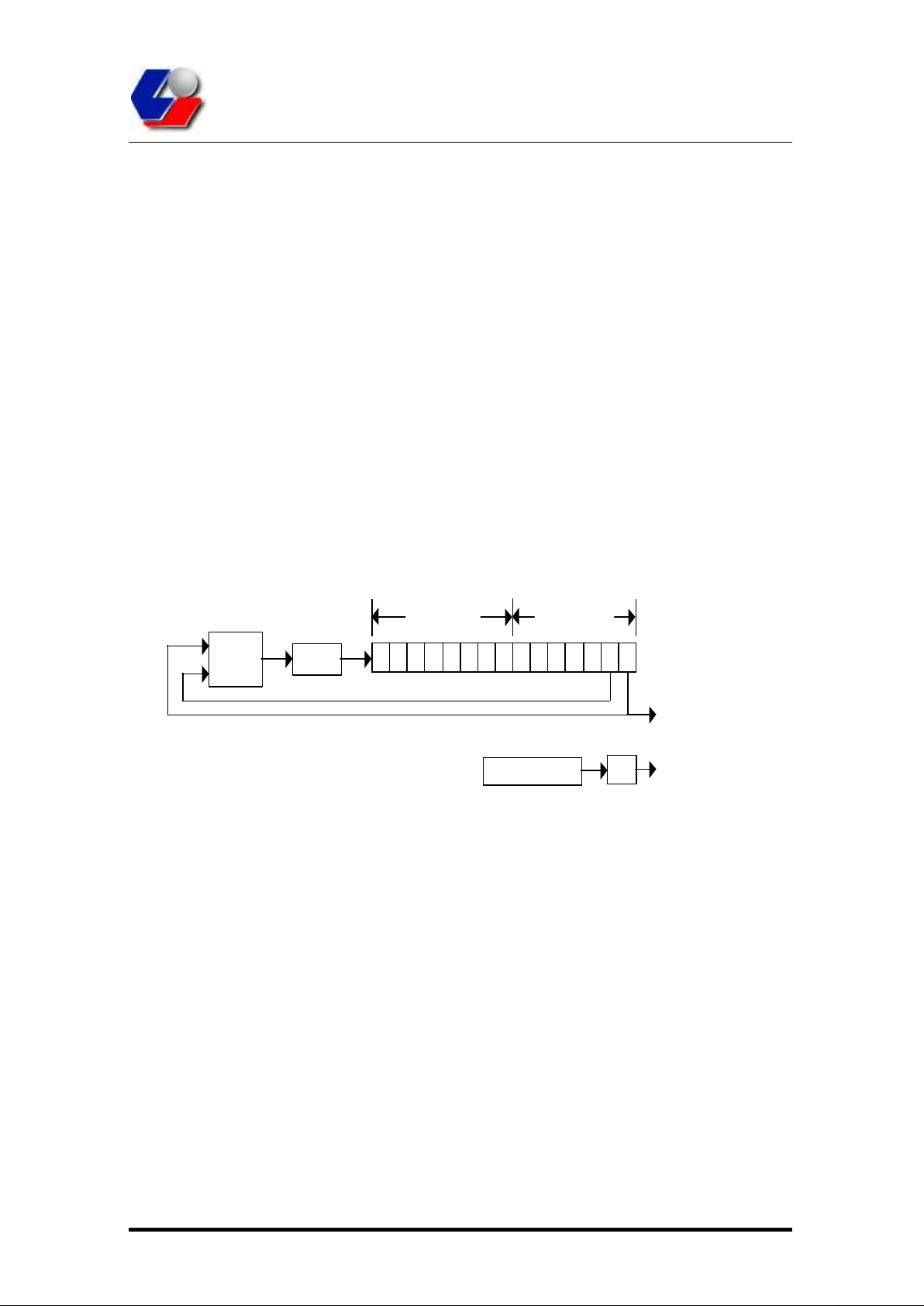
0093 Set sound generator 2 function. Write only.
Bit 0 : = 0 Sound generator 2 works in mode 0.
= 1 Sound generator 2 works in mode 1.
1 : = 0 Reset sound generator 2 counter.
NAND
S
0
1
MUX
SOUND
Page 8
Syntek Semiconductor Co.,Ltd.
Lcd Controller 8/ 15
STK55C321
= 1 Enable sound generator 2 counter.
2 : = 0 Disable sound generator 2 output to SOUND2 pin.
= 1 Enable sound generator 2 output to SOUND2 pin.
The default value is zero.
In mode 0, sound generator 2 work as a 15-bit pseudo random noise generator.
The shift direction is from LSB to MSB. The values of $0090 and $0091 don't
care.
In mode 1, sound generator 2 work as a 15-bit pseudo random counter. Its
initial value is defined by $0090 and $0091. A pulse will be output while 0000H
is encountered and the initial value will be reloaded. The output pulse will be
divided by two to output a square wave to SOUND2 pin.
4) Interrupts
* There are three interrupt sources :
NMI - Fix frequency (system frequency/16384) interrupt.
IRQ1 - Timer interrupt.
IRQ2 - External interrupt by port 2.
* Only IRQ2 will wake up CPU from power-down mode, but all interrupts will wake
up CPU from standby mode.
* If $0081 bit 0 is set to 1, an oscillator warm-up time (defined by $008B & $008C)
will be added before CPU been waked up. After wake up, programmer should clear
this bit.
* After CPU wake up from power-down mode, programmer should turn on LCD
0 1 2 3 4 5 6 7 0 1 2 3 4 5 6
NOTXOR
Output
(mode 0)
All bits = 0
1/2
Output
(mode 1)
Low byte
High byte
Page 9

Syntek Semiconductor Co.,Ltd.
Lcd Controller 9/ 15
STK55C321
again.
* If want to accept IRQ in the middle of NMI loop, please reset the IRQ disable flag
of the CPU before IRQ signal comes.
* In the IRQ routine, the program decide from the port $0083 which interrupt (timer
or port 2) happens.
* When port 2 in input mode and pin interrupt enable, a low signal from pin will
generate IRQ2.
5) Reset states
Register Initial value after reset
0080 0081 0082 uuuuuuu0
0083 00000000
0084 states on pins
0085 11111111
0086 states on pins
0087 11111111
0088 uuuu1111
0089 uuuuuuuu
008A uuuuuuuu
008B uuuuuuuu
008C uuuuuuuu
008D 00000000
008E uuuuuuuu
0090 uuuuuuuu
0091 uuuuuuuu
0092 uuuuuuuu
0093 uuuuu000
Note : u -- unknown
5. ABSOLUTE MAXIMUM RATINGS :
Operating temperature .................................................................. 0 to 70℃
Page 10

Syntek Semiconductor Co.,Ltd.
Lcd Controller 10/ 15
STK55C321
Storage temperature ................................................................ -65 to 150℃
Supply voltage ........................................................................................ 7 V
Input voltage ................................................................... -0.6 to Vdd+0.6 V
6. ELECTRICAL CHARACTERISTIC :
Parameter Symbol Condition Min Typ. Max Unit
Supply Voltage Vdd 2.5 3.0 4.0 V
Main system frequency ∅sys Vdd=2.5V 0.8 2 Mhz
Vdd=3V 2.7 Mhz
Vdd=4.0V 3.5 Mhz
Crystal frequency ∅cry 32768 Hz
Operating current Idd Vdd=4V,
∅sys=1Mhz
2 mA
Power-down current Idown Vdd=2.5V 0.2 µA
Vdd=3.0V 0.3 µA
Vdd=3.5V 0.8 µA
Vdd=4.0V 2 µA
Vdd=4.5V 8 µA
Vdd=4.8V 25 µA
Vdd=5.0V 80 µA
Vdd=5.25V 220 µA
Input high voltage Vih Vdd=5.0V 2.0 V
Input low voltage Vil Vdd=5.0V -0.6 0.8 V
Input high leakage current Iih Vih=Vdd -1 µA
Input low leakage current Iil Vil=0 1 µA
Output high voltage
(For SEGx and COMx)
Voh1 Ioh=-30µA Vdd-
0.2
Vdd V
Output low voltage
(for SEGx and COMx)
Vol1 Iol=40µA 0 0.2 V
Output high voltage
(for other pins)
Voh2 Ioh=-2mA Vdd-
0.4
Vdd V
Page 11

Syntek Semiconductor Co.,Ltd.
Lcd Controller 11/ 15
STK55C321
Output low voltage
(for other pins)
Vol2 Iol=2mA 0 0.4 V
Page 12

Syntek Semiconductor Co.,Ltd.
Lcd Controller 12/ 15
STK55C321
7. LCD WAVEFORM :
7.1 1/4 Bias, 1/8 Duty
1/frame frequency
Vdd
3/4 Vdd
2/4 Vdd
COM8 1/4 Vdd
Vss
Vdd
3/4 Vdd
2/4 Vdd
COM1 1/4 Vdd
Vss
Vdd
3/4 Vdd
2/4 Vdd
COM2 1/4 Vdd
Vss
Vdd
3/4 Vdd
2/4 Vdd
COM7 1/4 Vdd
Vss
Vdd
3/4 Vdd
SEGx 2/4 Vdd
1/4 Vdd
Vss
There are two LCD matrix DOTs active at (SEGx,COM1) and (SEGx,COM7)
Page 13

Syntek Semiconductor Co.,Ltd.
Lcd Controller 13/ 15
STK55C321
7.2 1/3 Bias, 1/8 Duty
1/frame frequency
Vdd
2/3 Vdd
COM8 1/3 Vdd
Vss
Vdd
2/3 Vdd
COM1 1/3 Vdd
Vss
Vdd
2/3 Vdd
COM2 1/3 Vdd
Vss
Vdd
2/3 Vdd
COM7 1/3 Vdd
Vss
Vdd
2/3 Vdd
SEGx 1/3 Vdd
Vss
There are two LCD matrix DOTs active at (SEGx,COM1) and (SEGx,COM7)
Page 14
Syntek Semiconductor Co.,Ltd.
Lcd Controller 14/ 15
STK55C321
Syntek Semiconductor Co., Ltd.
Customer Information Sheet for STK55C321 970926
1. Customer's Name : ____________________
2. Project title : _________________________
* 3. Syntek part number : ___________________
4. Package --------------- ( ) Chip ( ) 80-pin QFP
5. Options :
Oscillator type ----- ( ) RC ( ) XTAL
CPU freq. ---------- ( ) =Oscillator freq. ( ) =1/2(oscillator
freq.)
LCD duty ---------- ( ) 1/8 ( ) 1/4
LCD bias ----------- ( ) 1/4 ( ) 1/3
P o r t 1 P o r t 2
7 6 5 4 3 2 1 0 7 6 5 4 3 2 1 0
Pull-up
6. Customer code :
Code form ----------- ( ) EPROM ( ) file _______________
Checksum -----------9800-9FFF __________H
A000-AFFF __________H
B000-BFFF __________H
9800-BFFF __________H
7. Operating conditions :
All the operating conditions listed below are for Syntek reference. Syntek will not
guaranty on these values. Please refer to data book or contact Syntek for the guaranty
values.
Operating voltage : _____-_____ V Operating frequency : _____ Hz
Operating current : _____ mA Sleep current : _____ µA
Others :
Customer : __________________ Salesman : __________________Date : __/__/__
Page 15

Syntek Semiconductor Co.,Ltd.
Lcd Controller 15/ 15
STK55C321
Note : The items marked with '*' will be filled by Syntek.
 Loading...